CLASS D FIELD TIMEBASE
Although the class B output stage is efficient, especially when fitted with a flyback booster circuit, some energy is dissipated as heat in the two transistors of the output stage. An alternative and more efficient method of building up an analogue voltage or current waveform is to switch a d.c. supply into an integrator by means of a fast-acting chopper-switch working at high (compared to the alternations of the basic analogue waveform) frequency. The ratio of on-time to off-time in the switch determines how much energy is built up by the integrator. A class D field time base IC was developed along these lines. The TDA2600 contains a 150 kHz oscillator as chop-timer and an r.f. switch whose duty-cycle is varied according to a 20 ms ramp generated within the chip by conventional means.
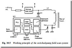
A later approach to switch-mode field scan technology is illustrated in basic form in Fig. 10.5, where the vertical deflection coils (yoke) have one end (A) permanently connected to a source of +21 V d.c. By varying the charge on capacitor C1, current can be made to flow through the yoke in either direction. As an example, variation of C1 charge between +30 V and +10 V in linear fashion over a 20 ms period would build up a sawtooth scanning current, symmetrical about Izero, in the coil.
The charge on C1 comes from winding X–Y on the line output transformer, which is so phased that during each line flyback period pin X goes 190 V positive of pin Y. If thyristor TH1 remains permanently off, diode D1 will act as rectifier and C1 will become charged to +190 V via L1. If, however, TH1 stays permanently on, LOPT pin Y is fully grounded: the pulse voltage at pin X positions itself symmetrically about ground potential (d.c. zero line) and the charge on C1 falls to zero. By varying the conduction period of TH1 the charge on C1 can be varied throughout the 20 ms field period.
Since TH1 is always turned off at the beginning of line flyback by the negative pulse from LOPT pin Y, its conduction period depends on the timing (phasing) of its positive gate turn-on pulse.
In this circuit, at the start of each field scan the TH1 trigger pulse comes late in each line, so a high voltage develops across C1; current flows fromB toA (conventional current flow) through the scan yoke. As field scan continues, TH1 trigger pulse timing (during each line period) is progressively advanced to linearly reduce C1 charge. Halfway through field scan (t = 10 ms) C1 charge equals +21 V and no current flows in the yoke; continuing advancement of TH1 gate pulse phase reduces C1 charge below +21 V, and an increasing cur- rent flows through the yoke from A to B. This reaches its maximum at the end of field scan (screen bottom) when TH1 gate pulses are cut off, C1 charge rapidly reverts to +190 V and a large current passes through the yoke in direction BA to give rapid flyback.
As Fig. 10.5 shows, the pulse generation and timing are carried out in IC1, type TEA2026A. The basic field scan timing is governed by a quartz crystal oscillator and phased to incoming field sync. To control the timing of the line-rate thyristor drive pulses a field-rate ramp is generated within the IC; its level is sampled at line rate in the field logic timing section. The sample level is processed in the field phase-modulator to form thyristor triggering pulses. This same IC is also responsible for sync separation; line flywheel synchronisation; line pulse generation; and control of the switch-mode power supply circuit.
