Audio amplification
Audio amplifiers invariably use the class D amplification mentioned in Chapter 14. The amplifier consists of a comparator driving two MOSFET transistors which operate as switches as illustrated in Figure 17.15. The comparator has two inputs. One is a triangle wave; the other is the audio signal. The frequency of the triangle wave must be much higher than that of the audio input. If the frequency of the triangular input is 20 or more times higher than the audio input, the output of the comparator is the
varying-duty cycle pulse (pulse width modulated, PWM) waveform shown. The output transistors Q1/Q2 switch from ‘full off’ to ‘full on’ and then back again, spending very little time in the linear region in between. Therefore, very little power is lost to heat. If the transistors have a low ‘on’ resistance, little voltage is dropped across them, further reducing losses.
It is necessary, however, to introduce a low-pass filter (L/C in the dia- gram) to the signal before amplification. The main reason for this filter is that the switching waveform results in maximum current flow. This causes more loss in the load, which causes lower efficiency. The LC filter with a cut-off frequency less than the class D switching frequency (typically 350 kHz), ensures that only the average of the output wave goes through, which is an amplified version of the input signal. In order to keep the distortion low, negative feedback is used. The disadvantage of class D amplifiers is the large output filter that drives up cost and size.
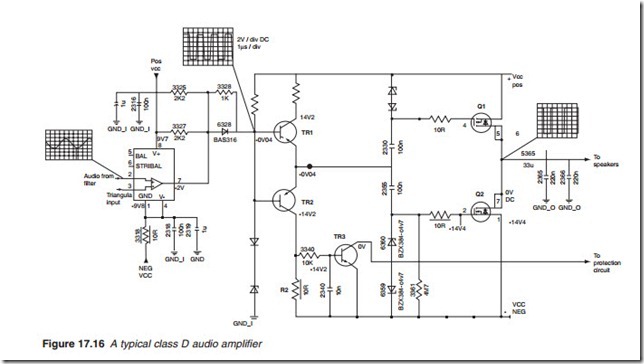
A typical TV audio amplifier circuit diagram is shown in Figure 17.16. Q1/Q2 package forms a class D complementary pair fed with ± 14 V d.c. Audio from the filter enters the voltage comparator from which a PWM waveform is produced. TR1 and TR2 are drive transistors and TR3 is a part of a high-temperature protection circuit. If the current through TR2 increases as a result of say a short-circuited output pair Q1/Q2, the voltage across its collector resistor R2 goes up, and TR3 conducts to activate a d.c. protection circuit (not shown). Because of the symmetrical supply, a d.c. blocking capacitor between the amplifier and the speaker is not necessary. However, it is still necessary for a protection circuit to protect the speaker from increased d.c. voltages.
