IC FIELD TIMEBASE
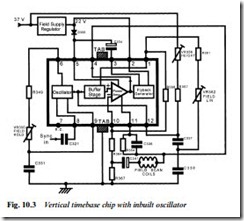
The field timebase, with its maximum internal power dissipation (in the case of a large-screen colour TV) of about 5 W, is amenable to encapsulation within a single heat-sinked IC like that illustrated in Fig. 10.3. The oscillator is triggered by field sync pulses coming into pin 8 via C321, and runs at a frequency determined by the RC time- constant of R349, field hold control VR350 and C331. The ‘switch- ing’ output from pin 12 is a negative pulse of 100 μs duration; it rapidly discharges the ramp-forming capacitor C337/338, which subsequently charges towards supply rail potential via R357 and height control VR356. The sawtooth wave thus formed is buffered within the chip to emerge at pin 1, where it is applied via R361 and linearity adjustment pot VR362 to the tap on the ramp-charging capacitor as a source of linearising feedback.
Pin 1 output passes through R368 to re-enter the IC on pin 10 as an input signal to the internal class B power amplifier. Its output, in the form of a ramp-down, appears at pin 4 and is applied directly to the field scan coils whose bottom end is grounded (a.c.-wise) by a large capacitor C341. R367 (1 Ω) samples coil current to produce a sawtooth voltage for reapplication to IC pin 10 as negative feedback. The gain of the output stage is determined by the ratio of input resistor R368 to feedback resistor R364.
The frequency response of this type of IC can extend well into the
r.f. range, and to prevent instability and parasitic oscillation the RC combination R354/C336 is included as a frequency-selective negative- feedback path to curtail h.f. response.
Flyback booster
During field flyback a high supply voltage is required for direct application to the scan coils in order to effect a complete reversal of current during the 1 ms flyback time available. A typical pair of field scan coils may have an L/R time-constant around 2 ms, calling for a supply voltage during flyback of roughly double that required for scan-period drive. To avoid the excessive dissipation in the upper half of the power output stage which would result from the provision of a ‘double voltage’ d.c. supply line, the flyback generator technique is used. During the forward scan pin 3 of the chip is at low potential, permitting C334 to charge to supply rail potential (about +20 V) via D305, which also supplies the output stage via pin 5. At the com- mencement of flyback a switch within the IC links pins 2 and 3, applying +20 V to the negative plate of C334. Since the capacitor cannot instantaneously alter its charge its upper plate now rises to 2 × 20 V = 40 V, reverse-biasing D305 and doubling the available sup- ply voltage at pin 5. When flyback is complete the switch reverts, enabling C334 to replenish its lost charge.
IC field deflector chip
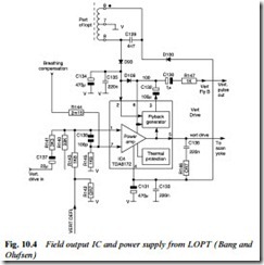
The provision of the vertical oscillator within the field output chip facilitates a simple design for basic and portable TV sets. In other types the oscillator and sync sections are incorporated within a ‘jungle’ chip like that of Fig. 7.7, leaving to the deflection IC only the functions of power drive to the yoke, and flyback generation. An IC of this type is shown in Fig. 10.4; it works to the same principles as the previous example, though the yoke-coupling capacitor is eliminated here because IC pin 5 is at zero volts in the middle of scan. It’s arranged by running the IC from ± 10 V lines derived from a special winding 6/7/8 on the line output transformer and rectifier/ smoothing sets D93/C134 (+10 V) and D100/C131 (–10 V). The flyback generator works in conjunction with booster C132/D109 to generate a pulse at IC pin 6 and rapidly pull the scanning beams back
to screen top. The pulse is also passed, via C130 and R147, to the teletext and blanking sections of the receiver. R146 and C136 perform the same functions as R354 and C336 in Fig. 10.3.
The deflection yoke current passes through R142 to ground, developing a sawtooth voltage at R143 for application to the inverting input of the IC at pin 1 as negative feedback: it stabilises picture height and confers good scanning linearity. Also applied to chip pin 1 is the sawtooth vertical drive waveform coming from the jungle chip via R140/R141/C137. The chip’s non-inverting input pin no. 7 takes an ‘anti-breathing’ voltage via R144 to compensate for the tendency of the picture to shrink at high tube beam currents.

