PLAYBACK LUMINANCE SYSTEM
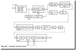
A simplified block diagram of the luminance playback process, taken from the same Panasonic machine as Fig. 14.2, is given in Fig. 14.4. This circuit is preceded by the replay head-switcher which selects the output signal of each head in turn as it scans the tape. Again the entire replay process is based on a single chip, IC3004. The two heads each have their own preamplifier, with adjustable resonant circuits to equalise the heads’ outputs and maximise them at about 4.9 MHz – any imbalance in their response or amplitude gives rise to some form of 25 Hz flicker in the replay picture. Correction for phase errors in the head- response shaping filters is provided by the phase-compensator block at the top left-hand corner. This is followed by a 627 kHz trap to remove all traces of the colour-under signal from the luminance f.m. waveform. Next comes the dropout compensator.
All videorecorders incorporate a dropout compensator. A dropout is a momentary loss of f.m. replay signal due to dirt at the tape/head
contact point or a minute imperfection of the tape surface. If uncorrected it gives rise to white or black streaks and dots in the picture. The correction process consists of substituting good f.m. carrier signal from the previous line, which will usually be very similar in video content. The amplitude of the replay f.m. signal is examined by a level detector, which triggers a switch when signal level falls below a preset point. The f.m. replay signal is continuously fed to a 1-line delay (between pins 10 and 12 of IC3004), and the switch changes over to the delay line output during a dropout. This delayed signal is recirculated through the line DL3001 and can be reused several times if the duration of the dropout is great. The use of dropout compensation greatly improves picture appearance, especially when old or worn tapes are in use.
The blocks to the right of IC3004 pin 10 are concerned with noise and interference elimination during momentary periods of loss of f.m. carrier, or severe amplitude-modulation of it, which almost amounts to the same thing. The resulting noise would cause disturbances on picture, especially at white/black transitions. To prevent these effects, a double-limiter circuit is used: the signal is split into two paths by filters, the high frequencies passing to their own amplifier and limiter between IC pins 14 and 6, for passage forward via adder transistor Q3020. Only the a.m. (noise) signal gets through the low-pass filter to be re-added in Q3020 to the high- level clipped f.m. signals; by this means the wanted f.m. signal level is kept within the operating range of the main limiter at IC3004 pin 14. This double-limiter technique is an effective and widely used one.
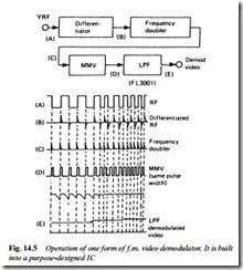
The main limiter ensures that the f.m. signal fed to the demodulator is free of all amplitude variations, an essential requirement for noise-free demodulation. The output voltage at pin 16 of IC3004 is proportional to carrier frequency, and as such forms the baseband video signal. The operation of the f.m. demodulator within IC3004 is illustrated in Fig. 14.5. The incoming f.m. signal (waveform A) is first differentiated to produce waveform B. A full-wave rectifier acts as frequency doubler to turn all the spikes positive – waveform C – in order that each can trigger a monostable multivibrator, which generates a pulse of fixed width on each spike, waveform D. As with the switch-mode field timebase and PSUs discussed in earlier chapters, we are now dealing with a waveform of varying duty-cycle, whose mark-space ratio reflects the amplitude of the required output signal. This is integrated (waveform E) to build up the output signal: as yet it is in somewhat ‘spiky’ form.
Returning to Fig. 14.4, the de-emphasis process follows demodulation, and is carried out in the blocks to the right of IC pin 16. During record the high frequencies of the luminance signal were boosted in a non-linear emphasis circuit (Fig. 10.2), and now balance is restored in a frequency-conscious replay network whose response, in terms of frequency versus amplitude, is the inverse of that used during record. In de-emphasising the video signal in an amplifier with falling h.f. response, much of the noise picked up during record and replay is eliminated – such noise is predominant in the upper frequency ranges.
Since the demodulator output is still in somewhat spiky form, and contains vestiges of the f.m. carrier waveform itself, the next process required is low-pass filtering to render a smooth luminance waveform. The filter is FL3001, whose response falls sharply at frequencies beyond 2.5 MHz. On emergence from this filter the luminance signal is fully balanced with regard to frequency distribution, but the reduced system bandwidth has degraded the rise and fall times of transients in the waveform, including the important sync pulse edges. The block marked Q3021, then, contains reactive components (or, in some videorecorder models, a complete delay-line-based crispener circuit as briefly described on page 132, Chapter 6) to sharpen up both picture transients and sync pulse edges.
After filtering and crispening, the processed luminance signal re-enters IC3004 on pin 25. Here it is applied to a noise cancelling circuit in which the high frequencies – containing most of the process- ing noise – are separated off and amplitude-limited. The limiter’s output consists largely of unwanted noise, interference and other spurious components: these are inverted in a following stage then added to the direct signal. In the adder stage the equal-and-opposite noise components cancel to leave a clean luminance waveform.
The noise-reduced luminance signal is now passed to a Y−C adder stage where it is recombined with the playback chrominance signal to produce a complete CVBS output. The chroma signal enters IC3004 at pin 29, and the resulting composite waveform undergoes treatment in the clamp stage. Here its d.c. level is stabilised, and here the synthesised field sync pulses are inserted as substitute for the jit- tering ‘real’ sync signal during still and trick modes where applicable. Also present at this point is a muting stage, brought into play whenever a disordered picture may be displayed: while the servo systems are locking up, when no control track pulse is present (e.g. replay of blank tape), or when the machine changes speeds during playback; the circuit of Fig. 14.4 is taken from a dual-speed videorecorder. Finally the CVBS signal passes through a record/playback switch on its way to IC output pin 2.
Possible refinements not detailed in Fig. 14.4 are luminance crosstalk compensation by means of a delay line and second demodulator; provision of a front-panel ‘sharpness’ control in which the crispening action may be controlled by the user; and the special circuits used in LP playback mode, notably for trick speed reproduction. The arrangements described are applicable in principle to any of the home video formats.


