Line timebase and drive
The purpose of the line timebase is to provide the appropriate deflection current through the line scan coils. As in the case of the field scan, the current waveform required to produce linear deflection is a sawtooth. However, at the relatively high line frequency, the reactance of the coil XL is very high compared with its d.c. resistance, so the resistance is insignificant. The line scan coils may then be treated as purely inductive. Given that VL is proportional to the rate of change of current (VL = LX(di/dt)) it follows that a linear current waveform in a pure inductor is obtained when a constant or d.c. voltage is applied across it. To obtain a sawtooth current waveform, the voltage waveform must be the pulse shown in Figure 13.21. For the scan period AB, the current is increasing at a small and constant rate. Consequently, voltage VL is a small positive value which remains constant for that duration. For the flyback period BC, the current is decreasing at a high and constant rate; VL is again constant but this time large and negative.
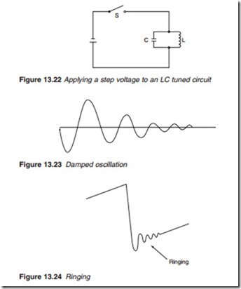
![]() Consider the tuned circuit in Figure 13.22. When the switch is closed, a step waveform is applied across the tuned circuit and energy is fed into it. Oscillation, known as ringing, takes place at a resonant frequency
Consider the tuned circuit in Figure 13.22. When the switch is closed, a step waveform is applied across the tuned circuit and energy is fed into it. Oscillation, known as ringing, takes place at a resonant frequency
f =1/2n LC
These oscillations take place because electromagnetic
energy in the scan coils is continuously transferred from electrostatic energy in the capacitor to electromagnetic energy in the inductor and vice versa. Current therefore flows from the coil to the capacitor and back again. Theoretically, this ringing would continue indefinitely since there is no power or energy loss in either a pure inductor or a pure capacitor.
However, due to losses caused mainly by the very small resistance of the inductor, ringing gradually dies out; producing what is known as damped oscillation (Figure 13.23).
Similar oscillation or ringing occurs when a sharp change in voltage is applied across an inductor. The tuning frequency in this case is the self- capacitance of the coil as well as any stray capacitance due to other components. In the case of the line scan, ringing occurs at the beginning of each flyback (Figure 13.24) with a consequent distortion on the left-hand side of the picture on the tube face.
It is possible to remove the effect of ringing by shunting the scan coils with a damping resistor. This, however, will result in a large waste of energy, reducing the power available for beam deflection and reducing the angle of deflection of the tube.
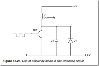
To avoid ringing but without the loss of energy, an efficiency diode may used. This technique is based on making use of the energy stored in the scan coils due to flyback to provide the first half of the scan. It involves a
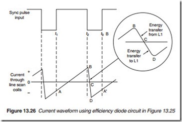
switching network which directs the transfer of energy to and from the scan coils to obtain the required waveform. A circuit using a parallel transistor-diode switch is shown in Figure 13.25, in which L1 is the scan coil, D1 is the efficiency diode and TR1 is the line output transistor. When TR1 is switched on by a positive edge to its base at time t1 (Figure 13.26), a constant h.t. voltage is applied across L1. A linearly increasing current is therefore obtained, forming part AB of the scan. The current continues to rise until point B, when at time t2 a negative step to the base switches off TR1. At this point, TR1 collector suffers a sudden jump from almost chas- sis potential to +h.t. This positive voltage ensures that D1 remains non- conducting. C1 is now effectively connected across L1. The large change in current in L1 produces ringing at a frequency determined by C1 and other stray capacitors. Energy due to the sudden change of current through L1 is transferred to C1 to commence ringing oscillation at point B. When C1 is fully charged (point C on the flyback), the charging current drops to zero as the ringing comes to the end of the first quarter-cycle of oscillation. The second quarter-cycle begins as energy from C1 is transferred to L1. The current reverses as the capacitor begins to discharge. When the cycle reaches its negative peak at the end of the first half-cycle (point D), the cur- rent begins to decrease, attempting to go to zero again. The rate of change of current di/dt suffers a change of direction. Before the negative peak (point D), the rate of change of current is positive. This induces an e.m.f. across L1, which makes TR1 collector (and D1 cathode) positive, ensuring the diode is off. At the negative peak itself, di/dt = 0 and the induced e.m.f. is also zero. After the negative peak, the current begins to decrease. The rate of change of current is therefore negative, reversing the induced e.m.f. and making TR1 collector (and D1 cathode) negative. The diode conducts. Its effect is similar to TR1 conducting, placing the h.t. across L1
to start the scan. Current through L1 rises linearly to form about 30% of the scan up to A’, when TR1 is switched on at time t3 by a positive edge to the base, and so on.


