Samsung single-chip solution
The single chip which caries all processing and formatting functions is a super video processor (SVP). Its functions may be summarised as follows (Figure 16.18):
● 3D colour decoder
● motion adaptive de-interlacing
● digital noise reduction
● image scaling
● APL
● dynamic picture enhancement
A typical configuration is shown in Figure 16.18.
Plasma panel power generation
With the exception of the plasma panel, power generation for FPDs follow very similar lines to those described in Chapter 15. The plasma panel is driven by high voltage, fast switching scan and sustain signals consume a large amount of power generating a large amount of heat. In such condi- tions it is essential to reduce the amount of heat generated and improve efficiency. In addition to high efficiency, PDP power supplies have to have fast transient response, low noise and low EMI.
A plasma display panel requires the following d.c. power supplies:
● Multi-power for processing chips, audio amplifiers and other semiconductors devices: 3.3 V, 3.6 V, +15 V, -15 V, 5 V.
● Address electrode power supply (70 V).
● Sustain and scan power supply (200 V).
A PDP power distribution system is shown in Figure 16.19. It consists of the following elements:
● main full-wave bridge rectifier,
● main line filter,
● power factor correction (PFC),
● multi-power supply for ICs, audio, etc.,
● sustain power supply VSUS,
● protection circuits (no shown).
Power factor correction, PFC reduces reactive power and introduces pre- regulation. The sustain power supply provide over 75% of the entire power requirement of the PDP. To ensure high efficiency, low noise and EMI, soft-switching resonant converters are used.
Power factor correction
The purpose of PFC is to reduce the reactive load current which is of no real value to the device. Only resistive power consumption is of any value as far as the device is concerned.
A fully resistive load when fed with a sinusoidal voltage is said to have a power factor of one. Power factor is defined as
If the voltage and current are pure sine waves, the power factor is given as k = Cos e, where e is the phase difference between the current and voltage waveforms. Since for a resistive load, current is in phase with the voltage, it follows that e = 0 and Cos e = 1. Hence the power factor k = 1.
For a purely resistive load, power P = Vrms X Irms. However, for a reactive load, the power factor has to be taken into account and power is given as
Thus, with a power factor (Cos e) of 0.5, only half of the power is useful power and the other half is completely wasted power.
A power factor of one is the highest power factor possible in which all power consumed by the device is useful power. On the other extreme, a purely reactive load, e.g. a pure inductor or a pure capacitor, has a power factor of zero since e = 90° and Cos 90° = 0. A power factor less than one can also be obtained if the voltage and/or current waveforms are not pure sinusoidal, if they contain harmonics, even though the load is resistive. This is the case with all types of rectification including con- trolled rectification. For this reason, the power rectification and supply circuits look reactive to the mains supply with a power factor of between 0.5 and 0.7.
To rectify this situation, PFC is employed to ensure that as little power as possible is wasted. Furthermore, under European law, mains harmonics are restricted for devices of 75 W and over. A PFC circuit is therefore needed to ensure that these harmonics do not exceed the permitted level.
A further reason for using PFC is to reduce the amount of imbalance on the three-phase mains power supply caused by low power factors.
Such interference becomes noticeable with high power requirements for equipments such as electric motors and PDPs. With PFC, a power factor of is possible.
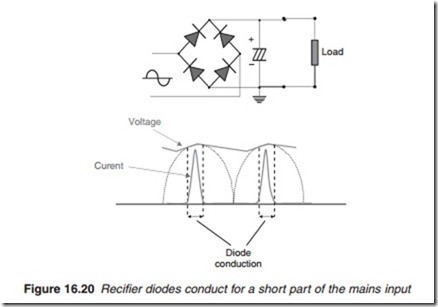
With the simple rectifier circuit illustrated in Figure 16.20, the diodes act as switches which conduct for a short period of time depending on the load current even if the load was fully resistive.
The current flows only when a pair of diodes conducts naturally, i.e.
when they are forward biased during the period when the instantaneous
value of mains voltages on their anodes exceeds the capacitor voltage on the cathode side. The current waveform is therefore a relatively narrow pulse as illustrated in Figure 16.20. While the fundamental of the current waveform is in phase with the incoming voltage, its harmonics are not resulting in a low power factor. This may be tolerated where power requirements are low (10s of Watts). However, when power consumption 306 Newnes Guide to Television and Video Technology
is high, in the region of 100s of Watts, then the losses due to low power fac- tors are high and must be avoided. This is carried out by a PFC circuitry. Instead of the capacitor receiving a charging current once every half cycle, PFC ensures that the charging current is small but more frequent; 100s of times every half cycle.
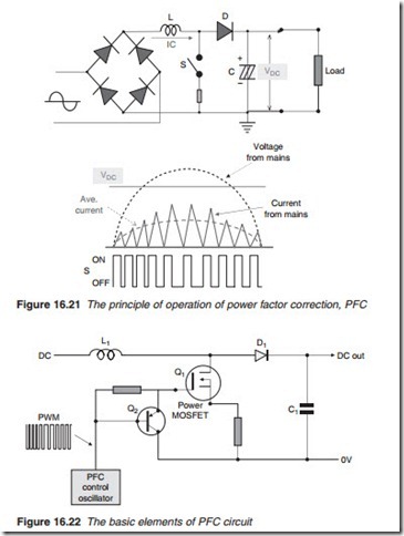
Figure 16.21 shows that when Switch S is closed, I flows through induc- tor L in a linear manner storing energy in the inductor. When S is open, current is abruptly cut and back e.m.f. across the inductor provides a for- ward bias to diode D, inductor L and capacitor C from a resonant circuit and charging current IC flows to charge capacitor C. Energy stored in the inductor is now transferred to the capacitor. When the capacitor is fully charged and IC is zero, diode D is reverse biased. At this moment, S is closed and current begins to flow through L and so on. The average cur- rent taken from the mains now follows the shape of the voltage as shown in Figure 16.21 resulting in a power factor as high as 0.85 or even 0.9. The switching waveform for S is the pulse modulated waveform shown with a frequency of 40–100 kHz. Note that the mark-to-space ratio of the PMW changes with the sine wave input. The off period increases gradually as the input goes up to peak and decreases as it goes down to zero while the ON period remains the same throughout.
The main element of a PFC circuit is shown in Figure 16.22. A power MOSFET, Q1 is used as the switching element. Q1 is driven by bipolar transistor Q2. The pulse width modulated (PWM) pulses are produced by the PFC control oscillator. The duty cycle is determined by the shape and
amplitude of the mains sine wave as well as the output voltage and cur- rent levels. In this respect, PFC acts as a voltage pre-regulator.
Figure 16.23 shows the main elements of a practical PFC circuit used by Panasonic employing two balanced MOSFETs for improved PFC.
Sine wave, current and DC output sensors are used to ensure that the cur- rent waveform follows as closely as possible the mains voltage.


