CHROMINANCE CIRCUITS
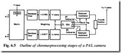
Fig. 6.5 shows in simplified form the colour circuits of the camera. The R and B preamplified chroma signals pass into a matrix where they are separately added to a −Y signal to render R−Y and B−Y components. Bandpass filters restrict these colour difference signals to a maximum frequency of 500 kHz on their way to be weighted. The weighting reduces the amplitude of R−Y and B−Y to prevent overloading of amplifiers and transmitters whose ratings are based on the standard 1 V pk-pk video signal. By reducing B−Y by a factor of 2.03 (becomes 0.493 B−Y, called U signal) and R−Y by a factor of 1.14 (becomes 0.877 R−Y, called V signal) the total excursion
of the CVBS signal is limited to max. 1.23 V on bright highly saturated colours, with the bottom tips of subcarrier cycles on highly saturated dark colours (i.e. blue, colour-bar pattern) 230 mV below black-level, as in Fig. 2.5. The U and V signals are now ready for encoding. First comes a clamping stage, whence the U and V signals enter the suppressed-carrier modulators, whose carrier inputs are derived from an IC-based SSG (Sync and Subcarrier Generator). The emerging modulated U and V signals come together in an encode balance control from whose slider is tapped off the chrominance signal complete. After gain control and amplification the chroma signal is added to the Y signal.
Generation of the swinging burst
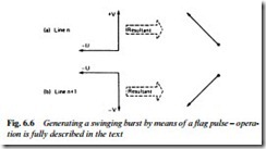
The V-axis subcarrier signal from the SSG already bears the required line-by-line phase reversals to conform with the PAL specification. The subcarrier feed to the U modulator is on the –U axis at all times, so that on line n the two available subcarrier feeds are as per Fig. 6.6(a), and on line n + 1 as per Fig. 6.6(b). If for the duration of the burst period the ordinarily balanced U and V modulators are permit- ted to become unbalanced, ‘carrier leaking’ takes place, permitting some carrier output to appear from the modulators even when no chroma input (the R−Y and B−Y channels are blanked during the back porch) is present.
The balancing of the modulators (embodied in a d.c.-coupled IC) is governed by their d.c. conditions, so that if a burst-flag pulse is applied to the modulator IC to upset balance, pure carrier will be permitted to leak into the chrominance signal, the amplitude of which will depend on the height of the burst flag pulse. Equal amounts of −U and (alternating) ±V are thus produced for the duration of the
burst flag pulse. In meeting at the slider of the encode balance control the vector-resultant of the two phases of the 4.43 MHz subcarrier are as shown by the phasors on the right-hand sides of Fig. 6.6(a)
and (b). In fact these are the very vectors required for the swinging burst signal – ±45° centred on the 180° (−B−Y) axis. To maintain the required 90° swing it is important that the leak-signal amplitudes are equal for both modulators; and to ensure correct burst amplitude (0.3 V, equal to sync pulse height in the CVBS signal) the height of the burst flag pulse is carefully controlled.

