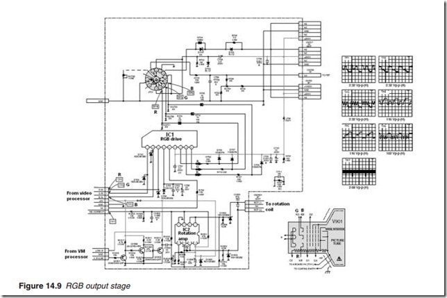
RGB output stage
With RGB drive, the output stage must be able to deliver a peak-to-peak signal of 80–150 V to the c.r.t. cathode. The signal drive to each gun is different because of the different efficiencies of the electrodes; the red gun requires the largest drive. The large signal drive requires a high d.c. sup- ply voltage and often two transistors are connected in series to share this high voltage. To ensure adequate bandwidth, series peaking coils may be employed. Power transistors in class A configuration are used with the necessary heat sinks to deliver the relatively large power necessary to drive the red, green and blue guns of the c.r.t. A small load resistance or an emitter follower buffer is used to ensure low output impedance. This low impedance allows for fast charge and discharge of the c.r.t.’s cathode input impedance, giving good frequency response at the upper end of the bandwidth.
Output stages are normally mounted on the c.r.t. base panel to remove the band-width limitations associated with long leads. Early output stages were also used for matrixing by feeding the luminance to the base and the colour difference signal to the emitter of the transistor. Black level clamping and brightness control of the three guns were also incorporated at the video output stage as well as greyscale adjustment. The purpose of
greyscale adjustment, or tracking, is to ensure that a purely monochrome picture has no traces of colour tint at any level of brightness from low- lights to highlights across the greyscale display. With the introduction of more advanced integrated circuits, matrixing is now carried out sepa- rately and clamping is introduced at the luminance signal channel before matrixing.
A typical RGB output schematic diagram for a 28-in. flat screen cathode ray tube (CRT) is shown in Figure 14.9 together with relevant waveforms. IC1 is the RGB drive chip and IC2 is the rotation amplifier providing the necessary S-correction as well as velocity modulation. RGB inputs arrive at pins 1, 2 and 3 of IC1 and following amplification they are fed to the tube neck panel pins 10, 9 and 8, respectively. Diode 707, 706 and 702 are reversed biased by 200 V d.c. to act as limiting diodes for the R, G and B signals going into the tube electrodes.
