Sub-field generation
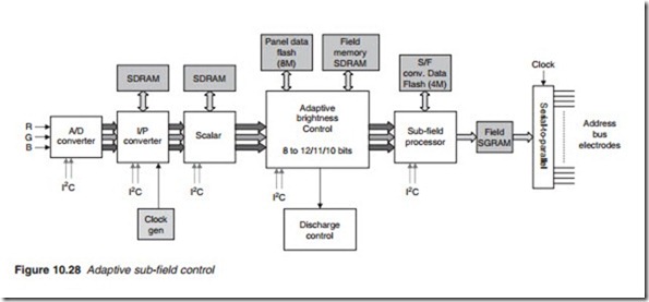
Figure 10.28 shows a block diagram incorporating the adaptive or dynamic brightness control technique. Analogue RGB signals are digitised by the A/D converter and following interlace-to-progressive (I/P) conversion, the digitised 24-bit video is fed to the scalar. The function of the scalar is to convert the format of the incoming video to the native resolution of the panel.
The converted video is then fed to the adaptive brightness control chip which determines the number of SF to be used, frame by frame and passes this information to the SF processor. It also synchronises the discharge of the pixel cells to control the sustain pulses and the duration of the dis- charge in line with the selected SF coding. A Flash memory holds the necessary software and a field memory stores the field contents. The SF processor produces the video information in the required bit stream to be stored in a Static Graphic RAM (SGRAM) memory chip before going into the serial-to-parallel converter to be clocked into the data electrode bus SF by SF. All processing chips are controlled via a serial control bus, normally an I2C from the microprocessor. For details of serial control bus I2C, se Appendix 2.
Alternate lighting of surfaces
In the conventional PDP construction, each pixel cell depends on two electrodes: scan and sustain. Discharge takes place between these two electrodes when a sustain pulse is applied across them. It follows that each line of pixels requires two strips of electrodes. As the panels resolution increases, the number of pixels per line and the number of lines increase demanding a much finer-pitched pixel cells. Furthermore, the number of electrode drivers has to rise which increases production costs. Another drawback of the conventional structure is the gap between electrode pairs that cannot be utilised for luminance radiation. While this structure is ade- quate for VGA-resolution PDPs, it is certainly impractical and costly for high-definition panels. Several developments have taken place in the con- struction of the pixel cells and the plasma panel to improve their high luminance efficiency and contrast ratio. These include alternate lighting of surfaces (ALiS) developed by Fujitsu-Hitachi.
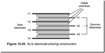
With ALiS, the Y electrode is shared between two X electrodes as illus- trated in Figure 10.29. The electrodes are arranged in equal intervals and
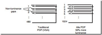
the space between them is used as display lines thus doubling the resolu- tion for the same number of electrodes. The non-luminance area between pairs of electrodes in the conventional PDP has been removed as shown in Figure 10.30, raising the aperture rate by 65% and improving luminance by 50.
Since each Y electrode is shared between two X electrodes, in order to ensure that each pixel line is independently addressed and discharged, interlaced addressing must be used. First the ‘odd’ field is addressed, line by line by energising pairs of electrodes in the following order: X1–Y1; X2–Y2; X3–Y3 and so on (Figure 10.29). This is followed by the sustain stage in which all pixel cells that have been selected in the ‘odd’ field are discharged. The same process is then repeated for the ‘even’ field by ener- gising the following pairs of electrodes: X2–Y1; X3–Y2; X4–Y3 and so on followed by sustaining the even filed. The whole process is then repeated for each individual SF. The interlaced driving of the PDP removes the need for interlace-to-progressive (I/P) converter. With ALiS, the number of elec- trodes required for a given number of pixel lines = ½ no. of lines + 1.
Compared with a conventional PDP, ALiS has higher resolution, brighter picture, lower cost, lower noise, longer life as the lighting duty of each cell is reduced by half as a result of interlacing and requiring no I/P conversion.


