IC-BASED SMPSU
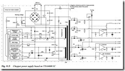
The majority of modern switch-mode power supply designs are based on a control IC incorporating a drive system, feedback regulator and protection circuits: a representative type is shown in Fig. 11.5. In essence it consists of a self-oscillating non-synchronous blocking converter whose frequency and duty-cycle automatically adjust to variations in mains supply voltage and loading of the output supply lines. The secondary voltages are stabilised to within 1 part in 200 over a mains input voltage range of 185 V to 265 V. For load variations between 30 W and 100 W the output voltages do not vary beyond ±1%.
IC631 (TDA4600) drives and controls the switching transistor T634 at frequencies between 22 kHz and 35 kHz, depending on input volt- age and load conditions. The start-up sequence of the IC is as fol- lows: first a coupling capacitor (C631) charge circuit is enabled, and an internal reference voltage of about 4 V is built up in the circuit connected to IC pin 1; this draws on the mains input supply via D616 and R616. As the IC supply voltage, coming via the same route, reaches about 12 V this internal reference voltage is switched to all sections of the IC. Finally the control logic is enabled and the chip begins to drive T634 via C631.
R621 limits the charging current of primary reservoir capacitor C626 at switch-on. IC631 starts from mains voltage via D616 and R616 at switch-on, but once PSU operation is stabilised it is powered from chopper transformer secondary winding 11–13 via D633 and C633; the action of D616 ensures that R616 current then falls. The 240 a.c.
IC is now held on by a bleed via R632 to pin 5 where a stand-by switch facility is provided: grounding this point will shut down the chopper supply, typically for use with a remote-control system incorporating stand-by facility. The shut-down/stand-by block within the IC also comes into action in the event of mains-supply undervoltage.
The 50 Hz a.c. supply voltage is full-wave rectified in diode bridge D621, smoothed by C626 and passed through protection fuse Si644 to form a +305 V operating line for the chopper system. It is applied to the primary winding (pin 7) of transformer TR651 whose bottom end (pin 1) is regularly grounded by main switcher T634. R646 and C646 provide a facsimile of the collector current to the IC at pin 4. C646 is permitted to charge whilst the transistor is on, and discharges whilst it is off. The ramp voltage thus formed at IC pin 4 is impressed on the base current amplifier within the chip and is used to drive T634 via IC pins 7 and 8, providing a base current proportional to the collector current, thus improving the transistor’s operating conditions and minimising power dissipation within it.
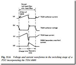
Winding 9–15 on the chopper transformer provides (by means of D647 and C647) a reference feedback voltage which reflects the actual line voltages developed by the diode-capacitor sets on TR651 secondary windings. It is applied to control pin 3 via set-voltage pot R647. R648/C648 prevent over-oscillation and consequent peaks on the switching edges. R644 and C641 feeds back to the IC information on zero-crossing conditions in TR651 so that the chopper transistor is not switched on until all the energy in TR651 has been transferred to the five output reservoir capacitors C652, 657, 662, 672 and 677. Fig. 11.6 shows relevant current and voltage waveforms in the circuit. At (a) appears the chopper transistor collector current which rises linearly during the charge time due to the inductance of TR651. The initial pulse is due to the action of C634, which smooths the falling edge of T634 collector voltage waveform at the beginning of each conduction period, see waveform (b); during the charge time T634 collector voltage is virtually zero. The base current driven into T634 by the IC is shown in waveform (c); it follows collector current due to the facsimile feed into IC pin 4. At a time controlled by the IC the base current is reversed to rapidly turn off T634, whose col- lector voltage rises sharply as a result. As collector current reduces to zero the energy stored in the chopper transformer TR651 is transferred into the various reservoir capacitors via the rectifier diodes on TR651 secondary windings. Waveform (d) shows the current waveform through main rectifier D656, which decays linearly to zero as the charge in C657 is fully replenished.
The diode current reaches zero when all the stored energy in TR651 has been transferred to the secondary reservoir capacitors and loads. At this point all the voltages across TR651 windings are at zero, and T634 collector is at primary supply voltage, +305 V, see Fig. 11.6(b). This condition is noted at IC pin 3, whose decay to 0.6 V triggers the chopper transistor on once more to repeat the cycle. This ‘stop-before- proceeding’ characteristic accounts for the fact that operating frequency depends on supply and demand conditions. The circuit runs at about 23 kHz under normal circumstances, rising to some 35 kHz under zero beam-current conditions. Inductors L633, L634 and capacitor C641 are included to prevent any tendency to self- oscillation at r.f., which would upset T634 operation and could cause spurious pattern pick-up at i.f., v.h.f. or u.h.f. frequencies.
The 12 V ‘+B’ line (and others) in Fig. 11.5 is provided by a series regulator of the type discussed earlier in this chapter. it is fed from the +M 19 V line, and takes the form of a three-legged IC. As with most such semiconductors its response reaches up to r.f. so decoupling capacitors C686 and C687 are used to ensure stability. LF decoupling thereafter is catered for by large capacitor C688, as it is for the other supply lines by capacitors C652, C657, C662, C672 and C677.
Internal overload protection is embodied in the TDA4600 IC in the form of an overload ident circuit connected to pin 3. This operates on the start stage and control logic to reduce drive to T634 in the event of abnormal conditions within the PSU or on the control- led output lines.
Mains isolation
Provided the chopper transformer is a well-insulated and high qual- ity component capable of withstanding a peak voltage of 5 kV between primary and secondary windings, it can fulfil a mains- isolating role, with the mains-live primary circuits (including the control IC itself) in a screened and protected section of the circuit board – or on a separate panel. The ground line of the TV or monitor itself can then be safely connected to true earth, exposed metalwork or other video/TV equipment. This is an essential feature of any piece of equipment to which direct connection of baseband audio and video signal feeds are to be made, and saves the provision and maintenance of special high working voltage isolating components in the aerial socket assembly. The circuit of Fig. 11.5 provides this mains isolation, the safety barrier being represented by the dotted line around the heavily shaded portion. The only link between the two is formed by the two small high-grade capacitors C611 and C613 which prevent the isolated chassis from drifting to some high potential with respect to true earth and mains neutral potential as a result of static charges.

