ALTERNATIVE CHOPPER CONFIGURATION
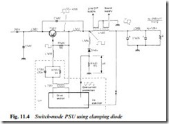
The arrangement of a power switch and energy reservoir can take several forms. Fig. 11.4 shows a quite different circuit in which the action is based on the clamping effect of diode D1464. The chopper- switch T1463 is turned on and off at its base by the control circuit so that its emitter rises to +290 V for the duration of t1, storing energy as a magnetic field in the ferrite core of inductor L1465. When T1463 is cut off during time t2 this field collapses, tending to push its left- hand terminal below ground potential. Such a move is prevented by conduction in D1464, which clamps T1463 emitter to approximately ground potential via low-value sampling resistor R1461. The volt- age at T1463 emitter now alternates between +290 V and 0 V. L1465 and reservoir capacitor C1406 form an integrator: at their junction
will appear an average value of the squarewave voltage at T1463 emit- ter. The voltage developed at L1466 is directly proportional to the ratio of t1 to the 64 μs (line-synchronous) switching cycle.
To stabilise the output voltage at C1406c against variations of input voltage and load, the 129 V output line is sampled against a reference voltage. When the drive section senses a rise in output voltage the duty-cycle of T1463 is reduced; if the output voltage falls the duty-cycle is increased. A protection function is provided by the sampling resistor R1461 as follows: an increase in current through the load increases the ripple current in D1464 and the correspond- ing ripple voltage across R1461. If this voltage (negative of ground) exceeds a predetermined level an overload is indicated and the drive section cuts off, switching off chopper T1463.
For T1463 to switch cleanly and enjoy low power dissipation its base drive current must be carefully controlled. In Fig. 11.4 drive transformer L7351 isolates the pulse-forming circuits from the 0–290 V switched emitter of T1463. Choke L1463 produces a negative pulse at the end of each base drive period to ensure fast turn-off. C1462 limits T1463 dissipation at that moment by its charging pulse from the +290 V line. Coupling capacitor C7351 ensures a sharp ‘attack’ in chopper base drive, speeding up switch-on and minimising dissipation in T1463. R7351 limits base current to a safe level thereafter.
The secondary winding on L1465 is a convenient point from which
to derive (via a rectifier and reservoir capacitor) a supply voltage for the audio amplifier section. A 20 V line is provided in this way. The other section of the secondary winding directly drives the base of the line output transistor, taking the place of the line drive transformer circuitry described in the previous chapter. It will now be obvious that the frequency and phase of the PSU drive section is critical, and must be flywheel-phased to incoming line sync pulses. In fact the switch-mode control IC (TDA2581) contains all the ele- ments of a line oscillator/sync section. In other designs the line output transistor is driven from a winding on the chopper transformer in the same way, but the SMPSU chip is synchronised to the output of a conventional line sync/oscillator IC. The use of a line-synchronous SMPSU avoids the risk of beat frequencies between line timebase and power switch, which could give rise to spurious beat patterns on the picture.
