TFT cell drive
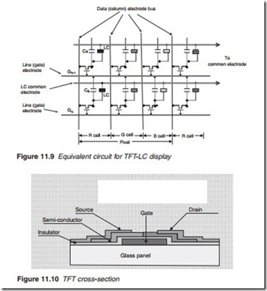
In the TFT LCD, switching transistors are provided for each pixel cell as shown in Figure 11.9. One side of each LC cells is connected to its own individual TFT while the other side is connected to a common electrode which is made of transparent indium tin oxide (ITO) material. This is necessary to ensure high aperture ratio. Aperture ratio is the ratio of the transparent area to the opaque area of the panel. A cross-section of a TFT is shown in Figure 11.10.
Unlike the CRT in which the phosphor persistence allows for continued luminance of the picture even after the electron beam has moved to scan other lines, in flat display applications, no such persistence exists and Data (column) electrode bus
refreshing of pixels to produce natural moving pictures becomes difficult as the number of pixels increases. Hence, the need for a pixel cell ‘mem- ory’. A charge on a storage capacitor CS is used for this purpose as illus- trated in Figure 11.9. Each cell consists of three sub-pixels (RGB) normally referred to as cells. Each cell contains an LC driven by a TFT acting as a switch. The LC is placed within two electrodes. One electrode is connected to the TFT’s source electrode and the other goes to a common electrode.
The TFT-LCD panel is scanned line by line. Each line is selected in turn by a VSEL pulse to the line (or gate) electrode bus. Once a line is selected, the pixel cells along that line can be addressed and their luminance levels set by a voltage applied via a source driver to their corresponding data (also known as source or column) electrode. The source driver supplies the desired voltage level known as the greyscale voltage representing the pixel value, i.e. the luminance of the pixel cell. The storage capacitor CS is charged and this charge maintains the luminance level of the pixel cell while the other lines are being scanned. When all the lines have been scanned and all the pixel cells addressed, the process is repeated for the next frame and the picture is refreshed.
Figure 11.11 shows the operation of an TFT-LC cell where GN is the cur- rently selected gate line and GN-1 is the immediately preceding gate line. The TFT gate is connected to the line (or gate) electrode bus, also known as the gate bus and the drain is connected to the data (or column) bus, also known as the source bus. Storage capacitor CS is connected between the current gate line GN and the immediately preceding gate line (GN-1). For this reason, CS is known as CS-on-gate. It forms the drain load for the TFT. The TFT turns fully on when its gate voltage is 20 V and turns off when its gate goes to at least -5 V. To select the pixel cell, a 20 V pulse, VSEL, is
applied to the gate. At the same time, data in the form of an analogue pos- itive voltage VDAT is applied to the drain. For peak white, VDAT is 0 V while for pitch black VDAT is a maximum of about 8 V. With the TFT on, the source and drain are shorted and VDAT is applied across the LC. The stor- age capacitor, CS-on-gate charges up and this charge is sustained even when the TFT is turned off. This is then repeated for the next line and so on. The main function of CS is to maintain the voltage across the LC until the next line select voltage is applied when the picture is refreshed. A large CS can improve the voltage holding ratio of the pixel cell and improve the contrast and flicker. However, a large CS results in higher TFT load and lower aperture ratio. In determining the value of the storage capacitance, account must be taken of the stray capacitance between the TFT’s gate and source, GGS which is effectively in parallel with CS.

