DVB satellite channel decoder
The precise construction of the channel decoder depends on the type of receiver, satellite (DVB-S) or terrestrial (DVB-T). For cable digital video broadcasting (DVB-C), the front end is similar to that used for satellite reception except for the input carrier frequency.
The function of the front end of a DVB STB is to extract the multiplexed transport stream from the modulated carrier received from a satellite dish or a terrestrial aerial. It consists of four stages:
● A tuner
● An analogue-to-digital converter (ADC)
● A demodulator: quadrature phase shift keying (QPSK) for satellite reception; orthogonal frequency division multiplex (OFDM) for terrestrial reception
● An FEC processor error correction
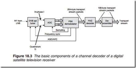
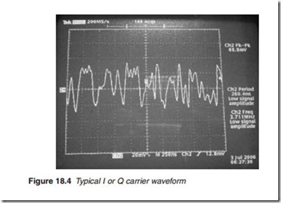
Figure 18.3 shows the basic components of a channel decoder of a digital satellite television receiver. The input to the tuner, a self-contained isolated unit, is in the form of a carrier known as the first IF from the LNB of a satellite dish. It is frequency modulated by a signal, itself a QPSK- modulated carrier. The tuner down-converts the input carrier to a second IF and reproduces the two original QPSK-modulated carriers: in-phase
(I) and quadrature (Q). The phase-modulated I and Q carriers have the distinctive waveform as shown in Figure 18.4. The I and Q carriers are
digitised by a dual-ADC (one for each carrier) into two 6-bit parallel streams. The sampling rate is set by a signal from the QPSK demodula- tor, which controls an in-built voltage-controlled oscillator (VCO). The sampling rate is normally set to twice the symbol rate; the symbol rate is the rate at which the phase of the carrier changes. The symbol rate itself is determined by the broadcaster and has to be set at the receiver before the tuner can select a channel. Thus, for a symbol rate of 27,500 kilo sym- bols per second (not to be confused with the 27 MHz video sampling clock), the sampling rate will be set at 2 X 27.5 = 55 MHz. Where the symbol rate is low, a sampling rate of three times the symbol rate is usu- ally used. Cable broadcasting uses a sampling rate of four times the symbol rate.
The demodulator carries out the phase detection of the I and Q signals, samples the recovered phases and quantises each phase change into a 3-bit code. The demodulator normally carries out several other functions including, AGC to control the gain of the tuner, control of the VCO and the sampling clock for the dual ADC.
As was explained in Chapter 17, the recovery of the original bitstream from a phase-modulated I and Q carriers involves two distinct stages: phase recovery and data recovery. Phase recovery identifies the phase change of the carrier and data recovery reproduces the original bitstream, a process known as symbol-to-bit mapping. The FEC decoder recovers the modulat- ing data bits from the QPSK carriers and arranges the information in a way that is suitable for presentation to the error detection/correction stage. The FEC error detection/correction stage consists of three parts. First comes a soft decision-making decoder, the Viterbi, which uses the original convolution coding to determine whether a received bit is logic 0 or logic
1. Next comes the deinterleaver; it rearranges the symbols and bits into the original order before they were interleaved at the transmitting stage. The final part is the Reed–Solomon (RS) decoder, which performs the hard decisions. Hard decisions determine whether a packet contains errors. If it does, the FEC unit will attempt to correct them. If it fails to do so, the FEC decoder will flag the packet as erroneous that must be discarded. At the end of the process, a transport stream that consists of a series of 188- byte transport packets is obtained. Before the transport packets are fed to the next demultiplexing stage, the pseudo-random energy dispersal is removed by a descrambler using the reverse of algorithms applied at the transmitting stage.
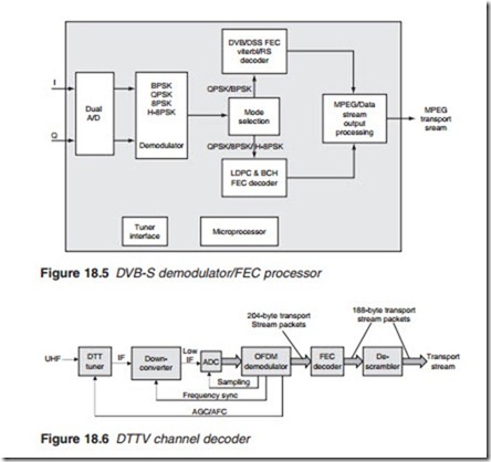
In practice, the dual-ADC, the demodulator and the FEC processor are integrated into a single package together with an embedded processor. The block diagram of a typical demodulator/FEC processing chip shown in Figure 18.5 is capable of processing BPSK, QPSK, 8-PSK and H-8PSK modulation. It has its own embedded dual DAC, tuner interface and microprocessor. I and Q carriers go in the input and a transport stream is available at the output.


