Computer Processors and Support:Power Supplies and Programmable Logic Devices

Power Supplies

It is surprising to many people that you can add a simple voltage regulator to power your projects for just a few dollars; cheaper than a set of rechargeable batteries. Voltage regulators, powered by an AC/DC ‘‘Wall wart’’ power converter, will convert one DC voltage to another that can be used by the electronics in your circuit and, more importantly, will be tolerant of changes in the AC supply and the current load. In this section, I will

introduce you to some simple power supply circuits that have the following characteristics:

1. They are safe for their users and designers.

2. They are relatively efficient in terms of the amount of power that is  lost converting voltage levels.

3. They provide very accurate voltage levels, independent of the voltage input or the current required by the application.

4. They are inexpensive.

5. Their design can be optimized for the application that they are providing power for.

6. These supplies source up to 1 amp of current.

The power supply ideas presented here are very appropriate for the simple circuits discussed in this book; the 250 watt power supply used for your PC requires methodologies and circuits for producing this much power that are quite a bit different than what is required for the simple power supplies presented here. Advanced degrees are normally required for properly designing high current power supplies that work at high efficiencies.

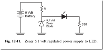
There are some semiconductor-based circuits, like Zener diode power supplies (Fig. 12-11) that do lend themselves to being modeled using water analogs. The Zener diode power supply works as a shunt regulator – applying a specified amount of current to a circuit at a rated voltage and shunting the rest away as wasted power.

When the term ‘‘shunt’’ is used, it is simply saying that excess voltage and current is turned away from the circuit. This concept can be illustrated with a water pressure regulator created from a catch basin with a hole at the bottom; water coming out of the hole is at a pressure which is determined by the depth of water in the basin. To maintain this depth (and bottom pressure), even though water is being drawn from the hole at the bottom, ‘‘source’’ water is continually poured into the basin. More water is pouring in than is expected to exit through the hole in the bottom, with the excess leaking out over the side. This is exactly how the Zener diode works, except

image

that extra current does not ‘‘leak out over the side’’ but is passed (or ‘‘shunted’’) through the diode. The diode itself is expected to be reverse biased when it is wired into the circuit and it will pass current through it to maintain a set voltage level at its anode (positive terminal). This property is known as ‘‘breakdown’’ and it is not unique to the Zener diode. All diodes will ‘‘breakdown’’ when a high enough reverse bias voltage is applied to them. The breakdown voltage for a Zener diode is usually specified to be in the range of 1.5–25 volts where the breakdown voltage for a typical diode (say the 1N4148/1N914 that I usually use) is 75–100 volts.

Specifying a Zener diode for use as a power supply in an application isn’t very difficult but it will require you to understand what your incoming power specifications are as well as what the required current is for the circuit being powered. The powered circuit’s voltage should be the same as the rating of the Zener diode. For 5 volt circuits, I use a Zener diode rated at 5.1 volts. Specifying the resistor that is to be used with the Zener diode as well as the Zener diode’s power rating can be somewhat complex. Care must be taken to ensure that the circuit has enough current to be powered in all circumstances, including if the input power ‘‘sags’’ (if it is powered by a battery that is discharging). To do this, some kind of ‘‘margins’’ must be designed into the circuit.

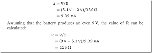
For this experiment, I would like to use a 5.1 volt Zener diode to act as a power supply for a LED circuit requiring approximately 10 mA to light the LED. The circuit is shown in Fig. 12-11 and, before it can be assembled, the value for the Zener diode’s current limiting resistor ‘‘R’’ must be determined. For a Zener diode power supply to be 100% efficient in terms of current (no current is shunted through the Zener diode), ‘‘R’’ must be chosen so that the voltage drop through it will allow the same amount of current as the powered circuit uses to pass through it. In this application, I am going to assume that the LED has a 2 volt drop, so using the basic electrical formulas, I can determine the current through the LED:

image

There are no standard 415 Q resistors available, but I can make a 420 Q resistor using a 200 Q and a 220 Q in series. This will result in a current of 9.29 mA (a difference of about 1% from the targeted value).

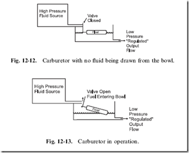
When I described the Zener diode regulator as acting like a basin of water in which the unused current was simply lost, I’m sure that many people grimaced because they knew of devices which are much better at regulating fluid pressure. If this book was written in the 1980s (or earlier) just about everybody would know about the commonly used fluid regulator that is used in older cars called a carburetor (Fig. 12-12). Virtually all cars built in the past 15 years have utilized some form of computer-controlled ‘‘fuel injection’’ which relies on active, rather than passive, control of the fuel being passed to the engine.

The carburetor is a very clever device that only provides fuel on demand. In Fig. 12-12, I have drawn the situation where no fuel is being drawn from the carburetor – a ‘‘float’’ is connected to a simple valve that closes when the fuel in the bowl that the float is in is full. When fuel is drawn from the bowl, the fuel level within the bowl drops (along with the float) and the valve opens, allowing more fuel into the bowl (Fig. 12-13). The carburetor is quite efficient and very simple in operation.

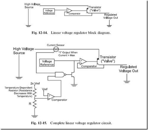
The carburetor acts as a regulator, just providing the volume of fuel (current) as required and the shallow bowl will result in lower pressure (pressure regulation) than what was available from the high-pressure source (the fuel pump). An electrical version of the carburetor would look

image

like Fig. 12-14; current from the high voltage source is switched through a PNP bipolar transistor, with the control of the transistor being the output of the comparator. The comparator’s inputs are the current voltage level of the regulator’s output and the specific ‘‘output’’ voltage which comes from some kind of voltage reference. The voltage reference is usually a Zener diode that has a miniscule amount of current passing through it; the comparator does not need a lot of current to operate.

Adding the current and temperature ‘‘crowbar’’ sensors is implemented something like in Fig. 12-15. When either the current output or temperature exceeds the preset limits, the reference voltage is pulled to ground using an NPN transistor (remember that the voltage reference is very low current so this can be done safely). In some regulators, if the current or temperature parameters are exceeded, they ‘‘latch’’ the failing state until power is removed and the crowbar conditions are reset. The need for the current sense and shut down should be pretty obvious to you; if the current drawn exceeds the

image

maximum rating for the PNP transistor, it could be damaged. The temperature sensor may be a bit more unexpected but shouldn’t be surprising when you consider what is happening in the regulator when it is transforming a high voltage into a lower one. The difference between the input voltage and the regulated voltage multiplied by the current being drawn by the circuit being regulated is the power dissipated by the regulator. For example, if you had a 12 volt voltage source and a 5 volt regulator providing 200 mA current, the power being dissipated by the regulator would be 1.4 watts. This level of power dissipation could damage the internal circuitry of the regulator or, at the very least, raise the temperature of the part so that it does not work as designed.

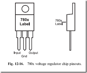
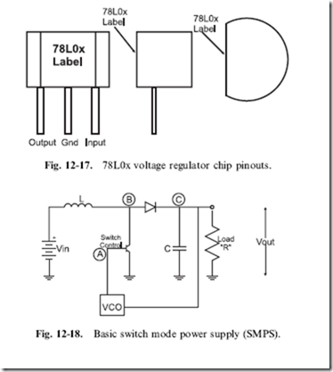
The most popular linear voltage regulators that provide the crowbar features are the 78xx and 78Lxx series. The 78xx (or the LM2940 series of regulators which have the same pinout and package) shown in Fig. 12-16 (‘‘xx’’ standing for the voltage, so a 5 volt regulator is a ‘‘7805’’) can normally source up to 500 mA and up to 1 A with heat sinking. The heat sink is used to dissipate the power and keep the temperature within the regulator less than 1258C, which is the crowbar temperature. For lower current applications (up to 100 mA), the 78Lxx (Fig. 12-17) can be used. For either device, the input voltage should be at least 2 volts above the regulated output voltage. When wiring the regulator in circuit, you should include at least 10 mF of capacitance on the input and a 0.1 mF capacitor on the output.

While the Zener diode and linear power supplies presented so far in this chapter are useful and easy to work with, they do have two concerns that can make them problematic when they are being used in a battery-powered application. First off, they require a higher voltage than the regulated output; this can be an issue when you want to use very simple power like two AA cells

image

for a digital electronics circuit. Secondly, they are not terribly efficient. It isn’t unusual for 80% or more of the power input to the Zener diode power supply to be lost and 40% or more lost in the linear power supply. What is required is a power supply circuit that is very efficient and will ‘‘step up’’ voltages.

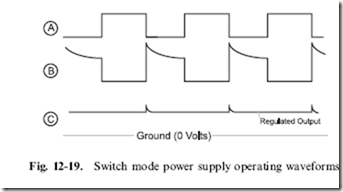
While these two requirements seem impossible, they can actually be achieved very easily through the use of the ‘‘switch mode power supply’’ (SMPS). The basic SMPS circuit (Fig. 12-18) is quite simple and relies on the energy storing characteristic of the inductor or ‘‘coil’’. While the capacitor stores energy in the form of charge, the coil stores energy in the form of a magnetic field which is maintained by current running through the coil.

When this current is shut off, the magnetic field produces a voltage ‘‘spike’’ (which I called ‘‘kickback’’ when discussing magnetic devices) that can be used as the basis for an output voltage.

Using the circled letters in Fig. 12-18, I have drawn the waveforms (Fig. 12-19) that you can expect to see in the SMPS. The ‘‘Control’’ signal is a PWM produced by a ‘‘voltage controlled oscillator’’ (VCO). A voltage controlled oscillator oscillates at a different frequency based on the voltage at an input. The input to the VCO used in the SMPS is the output voltage

image

image

of the power supply; the VCO frequency will change according to the power supply output to ensure the output stays as stable as possible at the required voltage. The output of the VCO is the base of a transistor that periodically pulls one side of the coil to ground, allowing current to flow through it. When the transistor connected to the coil is turned off, current flow through the coil stops and the magnetic field ‘‘kicks back’’, producing a higher voltage.

The operation of the VCO PWM output along with the coil’s response and the output voltage is shown in Fig. 12-19. When the VCO is turning on the transistor, the coil (symbol ‘‘L’’) is tied to ground and current flows through it. When the transistor is off, the coil kickback can be seen and any voltage greater than the current voltage output from the supply passes through the diode and is stored in the output capacitor. As I said above, if the output voltage is more or less than the target voltage, the VCO frequency changes along with the transistor control PWM, bringing the output voltage into line.

To determine the correct coil value as well as the PWM parameters, the following three formulas are used once the output voltage (‘‘Vout’’) is known along with the expected output current draw (‘‘Iout’’) and the input voltage (‘‘Vin’’). These formulas are used repeatedly until the values for ‘‘L’’ (the coil value), ‘‘Ton’’ (time the transistor is on) and ‘‘Toff’’ (time the transistor is off) are values that can be produced by reasonable hardware.

image

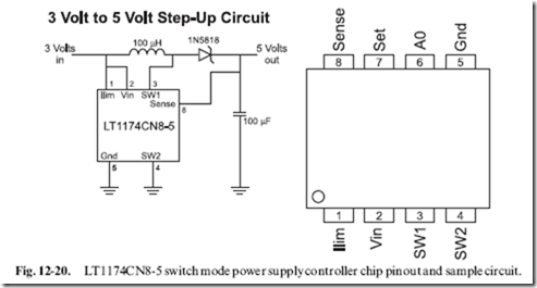
Designing an SMPS is not a trivial exercise. While you may think you can do it using something like a 555 timer, I’m going to recommend that you use a commercially available chip that provides the function for you, like the LT1173-5. This chip can be used to create 5 volts (neccesary TTL and

image

many CMOS logic chips) from 3 volts, as shown in the basic circuit in Fig. 12-20.

With the appropriate regulator selected, you now have to find a source of DC current to power the application and regulator. By far the most popular way of providing power to an electronic device is by simply plugging it into a wall socket.

I must caution you that the power coming out of your wall socket can conceivably destroy your application, cause a fire or hurt you (e.g. burns or electrocution). Despite the fact that it is commonly used for appliances, light and electronic devices in the home, electricity is not to be trifled with.

The circuits provided below may not be appropriate for where you live. The information provided here is strictly ‘‘rule of thumb’’ and is primarily written for use in North America. If you are going to design a power supply for a specific country’s use, make sure you understand what are the characteristics of the local power supply, along with any laws or regulations that are appropriate when connecting to it.

Power coming from your wall sockets (‘‘the mains’’), comes in as either a 110 or 220 volts ‘‘peak-to-peak’’ as a ‘‘sine wave’’ with a frequency of 50 or 60 cycles per second (or ‘‘hertz’’ (‘‘Hz’’)). In North America, power is provided at 110–120 volts peak-to-peak voltage (typically 115 volts) at 60 Hz. Different countries around the world will use different peak-to-peak voltage levels and operating frequencies.

This power coming in is normally provided by a ‘‘socket’’, which is built into your walls. Figure 12-21 shows the layout of the socket and labels the

individual connections. ‘‘Live’’ or ‘‘Hot’’ is the incoming alternating voltage sine wave shown in Fig. 12-21. ‘‘Neutral’’ is the return path for this current, while ‘‘Ground’’ is a shunt to ‘‘earth ground’’ if the circuit is damaged and the live voltage is passed to the neutral connection. If these three signals are being wired manually by convention, ‘‘Live’’ is black, ‘‘Neutral’’ is white and ‘‘Ground’’ is Green.

Because the AC voltage coming from the ‘‘mains’’ is so high and has

positive and negative voltage components, it has to be converted into a lower DC voltage for the electronics. This is done in three stages. The first is reducing the voltage from more than 100 volts to 15 volts or less using a ‘‘transformer’’. A transformer (Fig. 12-22) is a device made up of two coils that share their magnetic field. When current is passed through one coil, the second coil will produce an ‘‘inducted’’ voltage and current, which can be used to power the circuit. Figure 12-22 also gives the relationship between the voltage and current on the secondary side coil based on the number of turns for each coil.

Note that the current is inversely proportional to the turns ratio. In North America (which has 110 volts AC), an 8:1 transformer is often used. This means that with 110 volts in, there will be 14 volts out. For 220 volts, a 16:1 transformer should be used for the same voltage output.

While the voltage has been lowered, it is still ‘‘AC’’ and it is still going positive and negative. This voltage has to be ‘‘rectified’’ into a straight

image

DC voltage. This is done using diodes in either a ‘‘half wave’’ or ‘‘full wave’’ rectifier. Full wave rectifiers transform the positive and negative ‘‘lobes’’ of the AC circuit into a positive voltage, whereas the half wave rectifier ‘‘clips’’ the negative wave (providing half the total power available to the circuit). Inputting the rectified signal directly from the diodes into a voltage regulator should not be attempted; instead, a filtering electrolytic capacitor or a few tens of mF should be used. The filtered signal output from the full wave rectifier was shown in Chapter 3.

As long as the rectified signal does not drop below the minimum voltage of the Voltage Regulator, the regulated DC voltage output will be constant. The filtering cap should be a minimum of 10 mF with a good rule of thumb being that for digital circuits; a 20 mF capacitor is required for each Amp of current drawn. For DC electric motors, this value increases to 100 mF per amp drawn to help prevent inductive ‘‘kickback’’ ‘‘spikes’’ from being driven back through the transformer to the mains circuit.

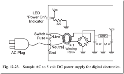
Using the transformer, full wave rectifier, an electrolytic filter capacitor and a 7805 voltage regulator, a þ5 volt 0.5 amp power supply for digital logic applications could be created, as shown in Fig. 12-23. The voltage regulator converts the rectified transformer-reduced AC voltage into a voltage that can be used by the digital logic.

There are a few things to note in Fig. 12-23. The first is that the mains ground is connected to the case and not to the ‘‘digital ground’’. In any DC- powered circuit, the negative terminal of the full wave rectifier can be called ‘‘digital ground’’, but should be left ‘‘floating’’ relative to ‘‘earth ground’’, which is provided by the AC plug. In this case, ‘‘digital ground’’ is simply a common negative terminal for the circuit. I have put a ‘‘fuse’’ in the power line, which will cut out in high current draw situations (like short circuits).

image

It is rated at 0.1 amps, which may seem low, but remember that current output is inversely proportional to the turns ratio of the transformer:

0.1 amps at 110 volts translates into 1.4 amps at 8 volts at the output. Without this fuse, very large (and very dangerous) currents could build up inside the circuit. For example, 2 amps at 110 volts translates to 28 amps at 8 volts or 224 watts of power. Along with the fuse, the ‘‘Switch’’ in the circuit should be one that is certified for switching AC voltages. AC switches usually have a mechanical assembly inside them that ‘‘snaps’’ the switch contacts on and off. This minimizes ‘‘arcing’’ within the switch. This may seem hard to believe, but if you look inside an AC switch while it is opening or closing, you will see a blue spark and sometimes hear a ‘‘pop’’. This is caused by high inductive voltages produced by the transformer coils that ‘‘kickback’’ when the AC power is shut off.

If you do build mains power supply circuits, like this one, I recommend that you use 14-gauge stranded wire for all connections. Connections should consist of soldered connections (not household ‘‘Marette’’ connectors) for safety. ‘‘Heat shrink tubing’’ should be placed over all solder joints and bare wire. As well, only UL/CSA (or the local country testing organization) approved plugs, wires, switches, fuse holders and transformers should be used in a properly grounded metal case.

If any of these terms are unfamiliar to you or you doubt your ability to build the circuit safely, then don’t build it!

Programmable Logic Devices

Programmable logic devices (‘‘PLDs’’) are chips which have logic gates and flip flops built in, but are not interconnected. The application designer will specify how the gates and flip flops are interconnected in order to create a portion of the application’s circuit. Most people feel that programmable logic devices are a relatively new invention, but they have been around for many years. It has only been quite recently (in the last 10 years or so) that reusable chip technology (i.e. EPROM and flash)-based PLDs have been available at prices hobbyists and small companies could afford.

There are several types of PLDs. The first is the simple array of logic gates and devices that are built of this type are known as ‘‘PALs’’ and ‘‘GALs’’ (I generically refer to them as ‘‘PALs’’). The chips themselves are quite simple and relatively easy to design circuits for. These circuits are normally arranged as a ‘‘sum of products’’ in which signals on the chip can be easily image
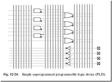
interconnected to form more complex logic functions. The chips are normally blocked out as a series of inputs and outputs, as shown in Fig. 12-24.

The vertical lines or ‘‘busses’’ in Fig. 12-24 are referenced to the gates and I/O pins they are connected to.

To form logic functions, the ‘‘sum of products’’ is used. In Fig. 12-24, a simple 4 I/O, 12 gate PAL is shown. Every output is driven on a bus in both positive as well as negative format. Connections are made between the gates and the busses to create logic functions.

For example, the ‘‘XOR’’ gate which is characterized by:

image

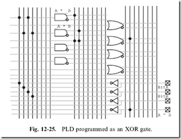
which is not often available in standard logic. Taking Fig. 12-24 and connecting the busses to the different I/O pins and gates within the PAL, I can implement the XOR gate, as shown in Fig. 12-25.

Note in Fig. 12-25, that an I/O pin changes from an input to an output by simply connecting it directly to a gate output. This feature allows the pins to be used as either input or output.

Options for PALs include varying numbers of inputs to the internal AND and OR gates. For the PLD shown in Fig. 12-25, I have left open the option that any of the pins can be used for any purpose. This is a bit unusual and, normally in PALs, the number of inputs to a gate is restricted. Another

image

option is to include built in flip flops to store states and turn the PAL from a combinatorial circuit into a sequential one.

PALs may seem simple, but they can result in large decreases in the chip count for an application. In some cases, PALs may be more expensive than the chips they replace, but they reduce application power and board space chip requirements. These savings could result in all-over product savings. It is not unusual for 10 TTL chips to be replaced by a single PAL, resulting in huge PCB and power supply cost savings.

At the high end of the programmable logic device family range, some

devices are virtually ‘‘ASICs’’ (‘‘Application Specific Integrated Circuits’’) and use the same programming language (‘‘VHDL’’) and development tools as ASICs. These complex parts generally have their functions broken up into ‘‘macros’’. An ASIC/PLD macro can be an AND, or XOR not, logic gate, flip flops or collections of functions (such as multiplexors and arithmetic logic units) which simplify the task of circuit development and eliminate the need for wiring individual gates into basic functions.

The high-end programmable logic device’s programming information is

often directly transferable to the technology. This allows initial production to use programmable logic devices that require little cost to program and, when the design is qualified, ASICs can be built at a chip foundry for reduced per unit costs.

Programmable logic devices have the advantage of being able to

implement fast (less than 10 ns) logic switching, but they do not have the ability to store more than a few bits of data.

Often, programmable logic devices are used in proprietary circuits because their functions cannot be easily traced and decoded.

Programmable logic devices and ASIC development tools are generally function text based as opposed to graphically based applications (like a schematic drawing). This means that a text format, like the ‘‘XOR’’ definition above, must be used to define the functions. Most ‘‘compilers’’ for these statements are intelligent enough to pick the best gates within the device to work with and pick the best paths without your intervention. They are typically much more sophisticated (and expensive) than the compilers used for converting high-level program statements into instructions for a processor.

Quiz

1. The choices in processor design are:

(a) Intel vs AMD vs PowerPC

(b) CISC vs RISC, Princeton architecture vs Harvard architecture, hardcoded instruction execution vs state machine instruction execution

(c) TTL vs CMOS logic

(d) Speed vs minimal power consumption

2. Microcoded instructions are:

(a) Short instructions which take less time to execute

(b) Coded instructions that cannot be read by spies

(c) Instructions that are specific to a microprocessor

(d) State machine instructions outlining the steps needed to execute an instruction

3. Decimal 47.123 in binary is:

(a) Invalid; you cannot perform this conversion (b) B’101111.00011111’

(c) B’11111.101111’

(d) 0x02F.1F7

4. Which statement is false? ‘‘Flash’’ memory cells:

(a) Are designed from EPROM memory cells

(b) Can be erased by applying an electrical voltage

(c) Are built from flip flops

(d) Are limited to 256 bits in size

5. DRAM Memory is:

(a) Faster than SRAM memory

(b) Less expensive per bit than SRAM memory

(c) More reliable than SRAM memory due to ‘‘refreshing’’

(d) More expensive per bit than SRAM memory

6. What is not a feature of the DC/DC power regulators presented in the book?

(a) They will convert AC to DC directly

(b) They have current limiting capability

(c) They have temperature limiting capability

(d) They have voltage ‘‘Brown out Reset’’ capability

7. With 12 volts coming in, the current limiting resistor for a 5 volt, 200 mA Zener diode:

(a) Insufficient information to calculate the resistor’s parameters

(b) 3.5 Q, 10 watt

(c) 350 Q, 1 watt

(d) 35 Q, 2 watt

8. A switch mode regulator needs the following components to work:

(a) Capacitors, diodes and inductor

(b) Capacitor, diode and PWM driver

(c) Capacitors, diode, transistor, PWM driver and inductor

(d) Comparator, PWM driver, transistor and inductor

9. ‘‘PAL’’ is the acronym for:

(a) Pound and lever

(b) Peripheral aspect light

(c) Partial AND logic

(d) Programmable array logic

10. VHDL is used for:

(a) Defining PLD electrical parameters

(b) Defining PLD gate requirements

(c) Defining PLD gate operations

(d) Defining PLD speed parameters
 

Computer Processors and Support:IEEE754 Floating Point Numbers and Memory Types

Computer Processors

and Support

I’m sure that you realize that computer processors are really just a great big sequential circuit, but I’m sure that you have no idea where to start understanding how they work. Traditional computer processors are designed using a selection of six or so basic design philosophies that give them different characteristics. In this chapter, I will introduce you to the different issues that have to be confronted in designing computer processors, along with some of the technologies that have been developed to support them.

From a high level, computer processor architects choose from making the processors ‘‘RISC’’ (‘‘Reduced Instruction Set Computers’’ – pronounced ‘‘risk’’) based or ‘‘CISC’’ (‘‘Complex Instruction Set Computers’’) based.

CISC processors tend to have a large number of instructions, each carrying out a different permutation of the same operation (accessing data directly, through index registers, etc.) with instructions perceived to be useful by the processor’s designer while RISC systems minimize the instruction set, but give them as much flexibility and access as much of the memory in the system

as possible. CISC processors also have the same requirement, but by definition, they are designed to simplify the amount of manipulation that is required by the programmer. Both computer types have their advantages and disadvantages – the RISC tends to be easier to design and executes instructions faster while the CISC tends to be easier to program but may be cumbersome in implementing some functions.

The second option processor designs have came from a competition

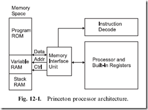
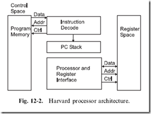
between Harvard and Princeton universities to come up with a computer architecture that could be used to compute tables of naval artillery shell distances for varying elevations and environmental conditions. Princeton’s response was for a computer that had common memory for storing the control program as well as variables and other data structures. It was best known by the chief scientist’s name ‘‘John Von Neumann’’. Figure 12-1 is a block diagram of the Princeton architecture. The ‘‘Memory Interface Unit’’ is responsible for arbitrating access to the memory space between reading instructions (based upon the current Program Counter) and passing data back and forth with the processor and its internal registers. In contrast, Harvard’s response (Fig. 12-2) was a design that used separate memory banks for program storage, the processor stack and variable RAM. By separating the data and program memories and avoiding the need to arbitrate data movements between them, there was an opportunity for programs to execute faster in Harvard’s computer.

It may at first seem that the Memory Interface Unit of the Princeton architecture is a bottleneck between the processor and the variable/RAM space – especially with the requirement for fetching instructions at the same time. In many Princeton architected processors, this is not the case because of the time required to execute an instruction is normally used

image

image

to fetch the next instruction (this is known as ‘‘pre-fetching’’). Other processors (most notably the processor in your PC) have separate program and data ‘‘caches’’ that can be accessed directly while other address accesses are taking place.

The Princeton architecture won the competition because it was better suited to the technology of the time. Using one memory was preferable because of the unreliability of then current electronics (this was before transistors were in widespread general use): a single memory and associated interface would have fewer things that could fail. The Harvard architecture is really best for processor applications that do not process large amounts of memory from different sources (which is what the Von Neumann architecture is best at) and be able to access this small amount of memory very quickly.

Once the processor’s instruction set philosophy and architecture have been decided upon, the design of the processor is then passed to the engineers responsible for implementing the design in silicon. Most of these details are left ‘‘under the covers’’ and do not affect how the application designer interfaces with the application. There is one detail that can have a big effect on how applications execute, and that is whether or not the processor is a ‘‘hardcoded’’ or ‘‘microcoded’’ device. Each processor instruction is in fact a series of instructions that are executed to carry out the instruction. For example, to load the accumulator in a processor, the following steps could be taken:

1. Output Address in Instruction to the Data Memory Address Bus Drivers.

2. Configure Internal Bus for Data Memory value to be stored in Accumulator.

3. Enable Bus Read.

4. Compare Data read in to zero or any other important conditions and set bits in the ‘‘STATUS’’ Register.

5. Disable Bus Read.

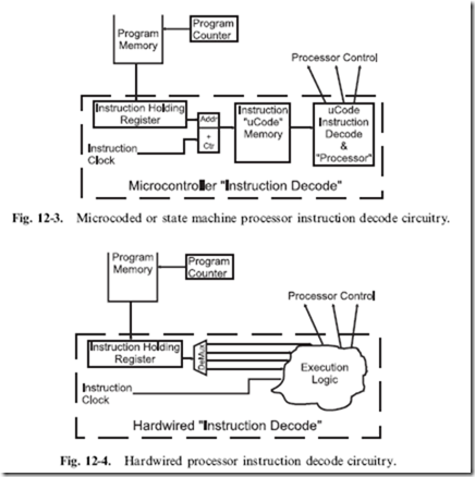
A microcoded processor is really a computer processor within a processor. In a microcoded processor, a ‘‘state machine’’ executes each different instruction as the address to a subroutine of instructions. When an instruction is loaded into the ‘‘Instruction Holding Register’’, certain bits of the instruction are used to point to the start of the instruction routine (or microcode) and the ‘‘uCode Instruction Decode and Processor’’ Logic executes the microcode instructions until an ‘‘instruction end’’ is encountered. This is shown in Fig. 12-3.

A ‘‘hardwired’’ processor uses the bit pattern of the instruction to access specific logic gates (possibly unique to the instruction) which are executed as a combinatorial circuit to carry out the instruction. Figure 12-4 shows how

image

the instruction loaded into the Instruction Holding Register is used to initiate a specific portion of the ‘‘Execution Logic’’ which carries out all the functions of the instruction.

Each of the two methods offers advantages over the other. A microcoded processor is usually simpler than a hardwired one to design and can be

implemented faster with less chance of having problems at specific conditions. If problems are found, revised ‘‘steppings’’ of the silicon can be made with a relatively small amount of design effort. The hardwired processor tends to execute instructions much faster but is much harder to modify.

IEEE754 Floating Point Numbers

When I introduced binary numbers earlier in the book, I discussed binary integers, but I did not discuss how binary ‘‘real’’ numbers were produced or how they were manipulated in workstation processors. It should not be a surprise to discover that binary floating point numbers are analogous to decimal floating point numbers.

For example, if you were going to convert decimal 7.80 to binary, you would first convert the value equal to or greater than one to binary.

Decimal 7 becomes B’0111’, leaving decimal 0.80 to convert. This is accomplished by knowing that decimal fraction digits are multiplied by negative exponents of the base 10. The same methodology can be used for binary numbers.

To convert decimal 0.80 to a binary fraction, I will start with the exponent ‘‘-1’’ which is equal to 0.5 decimal and test to see if it can be removed from the fraction. Since it can, my binary number becomes B’0111.1’ with a remainder of 0.30. Going to the next negative exponent (‘‘-2’’), I discover that I can subtract this value, giving me the binary value B’0111.11’. Continuing this on for another four bits, the binary value is B’0111.110011’. It’s interesting to see that the binary number is irrational; the bit pattern will change the smaller the fraction that is calculated even though the decimal number ends at the first digit after the decimal point.

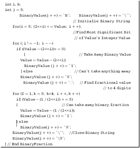
This method can be expressed as the ‘‘C’’ function, which converts the floating point number to a binary string:

image

image

This operation can be performed within high-performance processors (like the Intel Pentium), but instead of producing a string of characters represent- ing binary data, they generally put them into the IEEE754 format, which stores the floating binary value in a format which is similar to that of ‘‘Scientific Notation’’:

image

The ‘‘Mantissa’’ is multiplied by the signed exponent to get values less than or greater than one.

image

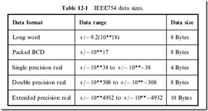
Table 12-1 lists the data formats supported by the Intel Pentium. These different formats give you a lot of flexibility to work with a wide range of numbers in different applications. All the number formats can be processed together, with the final result being in the most accurate format (i.e. a ‘‘word’’ and ‘‘single precision’’ combined together will have a result as a single precision number).

Memory Types

A number of different memory types are currently available. In this introduction, I will first show you three different technologies and discuss where (and why) they are used in a computer system. The boot up, non-volatile memory used in a computer system is based on ultraviolet light ‘‘Erasable PROM’’ (‘‘EPROM’’) program memory (Fig. 12-5) and was first introduced in the late 1960s. An EPROM memory cell consists of a transistor

image

that can be set to be always ‘‘on’’ or ‘‘off’’. Figure 12-5 shows the side view of the EPROM transistor.

The EPROM transistor is a MOSFET-like transistor with a ‘‘floating’’ gate surrounded by silicon dioxide above the substrate of the device. ‘‘Silicon dioxide’’ is best known as ‘‘glass’’ and is a very good insulator. To program the floating gate, the ‘‘Control’’ gate above the floating gate is raised to a high enough voltage potential to have the silicon dioxide surrounding it to ‘‘break down’’ and allow a charge to pass into the floating gate. With a charge in the floating gate, the transistor is turned ‘‘on’’ at all times, until the charge escapes (which will take a very long time that is usually measured in tens of years).

An improvement over UV erasable EPROM technology is ‘‘Electrically Erasable PROM’’ (‘‘EEPROM’’). This non-volatile memory is built with the same technology as EPROM, but the floating gate’s charge can be removed by circuits on the chip and no UV light is required. There are two types of EEPROM available. The first type is simply known as ‘‘EEPROM’’ and allows each bit (and byte) in the program memory array to be reprogrammed without affecting any other cells in the array. This type of memory first became available in the early 1980s.

In the late 1980s, Intel introduced a modification to EEPROM that was called ‘‘Flash’’. The difference between Flash and EEPROM is Flash’s use of a bussed circuit for erasing the cells’ floating gates rather than making each cell independent. This reduced the cost of the EEPROM memory and speeded up the time required to program a device (rather than having to erase each cell in the EEPROM individually, in Flash the erase cycle, which takes as long for one byte, erases all the memory in the array).

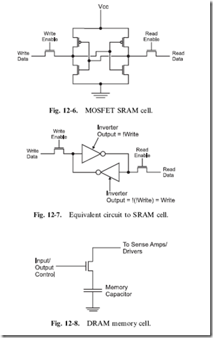
For high-speed storage, data is saved in ‘‘Static Random Access Memory’’ (‘‘SRAM’’) which will retain the current contents as long as power is applied to it and is known as ‘‘volatile’’ memory. This is in contrast to the ‘‘EPROM’’ or Flash, which does not loose its contents when power is taken away but cannot have its contents changed as easily as ‘‘SRAM’’. Each bit in a SRAM memory array is made up of the six transistor memory cell, as shown in Fig. 12-6. This memory cell will stay in one state until the ‘‘Write Enable’’ transistor is enabled and the write data is used to set the state of the SRAM cell.

The SRAM cell could be modeled as the two inverters shown in Fig. 12-7. Once a value has been set in the inverters’ feedback loop it will stay there until changed. Reading data is accomplished by asserting the read enable line and inverting the value output (because the ‘‘read’’ side contains the inverted ‘‘write’’ side’s data). The driver to the SRAM cell must be able to ‘‘overpower’’ the output of the inverter in order for it to change state.

image

The outputs of the inverters are usually current limited to avoid any backdriving concerns.

Large, inexpensive and reasonably high-speed memory can be built from ‘‘Dynamic Random Access Memory’’ (‘‘DRAM’’) cells. You may have heard the term ‘‘Single Transistor Memory Cells’’ for descriptions of DRAM and that’s actually a pretty good description of each cell, which is shown in Fig. 12-8.

In DRAM memory cell, the transistor is used as a switch to allow a charge to be moved into or out of the capacitor. For a write, the transistor is turned on and a charge is either pushed into or pulled out of the capacitor. When the transistor is turned off, the charge is trapped in the capacitor and cannot change until the transistor is turned on again.

A DRAM read is accomplished by turning on the transistor and any charge that is in the capacitor will leak out and will be detected and amplified by a ‘‘Sense Amplifier’’. The ‘‘Sense Amp’’ is a metastable flip flop that will be set to the state of the capacitor when the transistor switch is closed. Before the transistor is turned on when writing to the cell, the sense amp will be set to a specific state to load the correct charge into the capacitor.

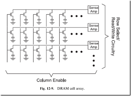
In a DRAM memory chip, the cells are arranged in rows and columns, as shown in Fig. 12-9. To address each cell within the chip, a row/column address for the element in the array has to be provided. Usually, to save pins on the DRAM chips, the row and column address lines are shared (multiplexed) together so that during a read or a write, first the ‘‘Row’’ is selected and then the ‘‘Column’’.

The row is selected first so that if a write is taking place the sense amp for the row can be set to the specific value. All the other sense amps are set in their metastable state. When the Column address is latched in, the transistors for the array row are turned on. Next, when the row address is available, the

image


image

place. For the cells not being written to, the sense amps will not only read what the charge is in the capacitor but will also ‘‘refresh’’ it as well.

This is a very good thing in DRAM because the capacitor is actually a MOS transistor built into the chip, acting as a capacitor. Over time, any charge in this capacitor will leak away into the silicon substrate. By periodically ‘‘refreshing’’ the charge by performing a read (which will cause the sense amps to amplify the charge), the contents of the memory will never be lost.

Refreshing is typically done by enabling all the transistors in a column (without first specifying a row) and letting the sense amps do their thing. A read of an incrementing column address is usually implemented in the DRAM support hardware and is known as a ‘‘CAS (‘‘Column Address Strobe’’) Only Refresh’’. In the original PC, 5% of the processor bandwidth was lost due to DRAM refresh requirements. To overcome these potential deficiencies, PC designers have come up with a few hardware features.

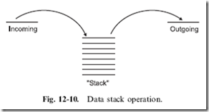
Along with being arranged as simple, single-dimensional arrays of data, memory can also be built into ‘‘stacks’’ (Fig. 12-10). Processor stacks are a simple and fast way of saving data during program execution. Stacks save data in a processor the same way you save papers on your desk and is known as ‘‘last in/first out’’ (‘‘LIFO’’) memory. As you are working, the work piles up in front of you and you do the task that is at the top of the pile.


Reading Datasheets : Chip Operating Characteristics , IEEE Logic Symbols and Power Usage and Fanouts

Reading Datasheets

I’ve never understood why college and university courses do not give an introductory course in reading digital electronic device datasheets. Despite how prepared you are for them, you will feel quite overwhelmed the first time you have to look through a number of datasheets trying to find a part that meets your requirements. When I first started working with electronics, datasheets were generally quite poor, with only a few standout companies providing good documentation for their chips. Fortunately, this has changed over the past 10 years, the Internet and the capability of downloading good- quality datasheets being almost a marketing tool to help engineers select the parts they are going to use in their designs.

Personally, I find it more daunting to look at datasheets over the Internet because they are generally encoded as Adobe Acrobat pdfs that take a while to load and you can never flip the pages on the screen as fast as you would like. To make matters worse, it can be very difficult to put multiple datasheets up on a computer display to allow you to compare the features of the different chips. This difficulty gives rise to the most important recommendation that I can make about downloading datasheets from the Internet – print them out! I have several binders of printed out datasheets for parts that I often use. By printing them out, I have immediate access to them and I can flip back and forth between pages effortlessly. It is my opinion that documentation shouldn’t be ‘‘paperless’’.

The first sheet of the datasheet is usually a one page description of the part. It normally contains:

1. Part number

2. High-level part description

3. Part pinout

4. Common/related/pin compatible parts

5. Important chip features

6. Basic operations truth table

When looking at a datasheet, you should first check out the part number of the datasheet versus what you are interested in. This means that you should be checking not only the numeric code for the device but also the high-level identifier and the technology identifier. For example, if you were looking for a low-power TTL dual input NAND gate and looked up the datasheet based on a web search for ‘‘TTL dual input NAND’’, you could see such diverse part numbers as:

74LS00

74C00

54LS00

74W00

74ALS03

with the question being: Which is the one that you want?

For these parts the high-level identifier is the ‘‘74’’ or ‘‘54’’. In this book, I have focused on the 74 series of logic – but if you look at ‘‘54’’ series logicyou will see that its operation is identical and may decide to go ahead and order the parts. This could be a big problem because ‘‘54’’ series parts are military-grade chips and they tend to cost 10 times that of standard ‘‘74’’ series logic and do not necessarily have the same pinout as ‘‘74’’ series chips.

The technology identifier is the letter code between the high-level identifier and the part number. In the list of five chips above, I have presented traditional TTL low-power logic (‘‘LS’’), CMOS logic (‘‘C’’), advanced Shottkey low power (‘‘ALS’’) and single gate CMOS (‘‘W’’). The danger of not reading the datasheet’s part number is that you could end up ordering the wrong part number, resulting in higher than expected costs and lost time looking up and reordering the correct part.

Always read through the datasheet’s first page high-level part number description. This can range from a single sentence to four or five bulleted items. Like the part number check, this should just be a filter operation, resulting in you making sure the part will do essentially what you want it to do.

The part pinout is something that is critical to know when you are wiring a circuit. Except for the wiring experiments presented in this book, I have

listed only a few part pinouts because a part’s pinout may vary between manufacturers of the same part and they may vary according to the packaging type. The part pinout may also change according to packaging technology. It isn’t unusual to see a pin through hole (PTH) packaged chip with a specific pinout but its surface mount technology (SMT) sibling having extra pins or different connections to different pin numbers. I’m sure that both of these statements are a bit hard to understand; you might be thinking that the part numbers are standard. I wish I could tell you how many times I have been bitten by these two little traps. Circuit design systems also make assumptions about part pinouts based on the pinouts from specific manufacturers and don’t bother checking the pinouts from others.

The important chip features listed on the front page of the datasheet will not list the features of the chip to the lowest possible level, but it will give you some ideas about how the chip works and if there are any issues that could be a problem with you using the chip in your application.

A lot of times you will discover that a part will not have exactly the functions that you want but, by checking the datasheet, it may list related parts that provide a similar function that you can take a look at. Finally, for very simple chips, the front page of the datasheet will present you with truth tables describing the operation of the chip or the different parts of the chip.

The front page of a chip’s datasheet can be incredibly useful to you and by spending a few minutes familiarizing yourself with it, you can decide whether or not the chip is appropriate for your application without having to delve into the minutia of the following pages.

Chip Operating Characteristics

An important feature of the datasheet is the ‘‘operating characteristics’’ for the chip. This section of the datasheet explains such operating parameters as:
1. Input pin voltage thresholds and currents

2. Output voltages along with current source and sinking capabilities

image

3. Gate delay timing

4. Expected input and output pin line impedances

5. Miscellaneous operating information.

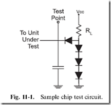
Each chip datasheet lists the logic thresholds, along with their characteristics when subjected to different parameters. Often you will see a two-axis graph, with a curve showing the chip characteristic response to the changing input parameters. This part of the drawing should not be difficult to understand but what can be confusing is the small schematic marked as a ‘‘test circuit’’ that often accompanies the graph. An example of such a schematic is shown in Fig. 11-1; it shows the circuit that was connected to the pin while the test was taking place. These test circuits simulate other circuits connected to the chip, helping to ensure that the chip is operating as it would in a typical application.

The output voltage and current characteristics are really a function of the logic technology used and not unique to the individual chip’s pins.

If you were to read other datasheets of chips built from the same technology you would discover that the output parameters are the same between the two chips and, by extrapolation, all the chips built from this technology. If you were to search the manufacturer’s web site, you would discover that this information has been published for all parts in the technology family and the information in the chip’s datasheet is really redundant. The reason why the information is repeated in the individual chip’s datasheets is to minimize the amount of cross-checking that you will have to do.
The previous comment could be made about gate delay timing but there is a wrinkle in the specification in the datasheet. Is the quoted ‘‘gate delay’’ for the chip function or for the individual basic technology gate (i.e. the ‘‘NAND’’ gate for TTL)? Normally, the datasheet will list the chip function gate delay instead of the basic technology gate delay because the actual gate delay is probably less than the product of the basic gate delay time multiplied by the number of gates the signal has to pass through.

As you learn more about electronics, you learn that not only do wire connections have resistance but they also have capacitance and impedance.

All these factors affect the transmission of data signals and are known by the term ‘‘characteristic impedance’’. Printed circuit boards (PCBs) have a characteristic impedance of 55 Q (the coax cable that sends signals to your TV has a characteristic impedance of 75 Q). The input and output pins must be designed to match with the 55 Q PCB characteristic impedance to ensure that signals pass between pins as efficiently as possible.

All these chip characteristics and any miscellaneous data that the chip manufacturer feels important enough to include should be read through and understood in order to best wire a chip into your application circuit.

IEEE Logic Symbols

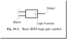
When you look at some datasheets, you will see the function of the chip described using a graphical system that is different from the one that I have used in this book. Instead of unique shapes for each gate, they are represented as a rectangular block like the one in Fig. 11-2. These blocks are part of the ‘‘IEEE Standard Graphic Symbols for Logic Functions’’. This standard is often used to describe the operation of a chip instead of the graphical symbols that I have used in the book.

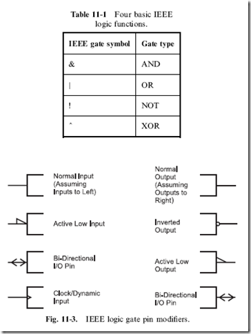
The IEEE gate definition contains a single character to indicate what the function is. Table 11-1 lists the basic characters and their functions. For

negated outputs and inputs, the gate pin modifiers presented in Fig. 11-3 are used. Note in Table 11-1, only the four unique gate functions are listed – NAND and NOR gates are represented with the gate modifiers shown in Fig. 11-3.

image


image

For the complete IEEE logic symbol definition, I suggest that you download and printout ANSI/IEEE Std 91a-1991 from:

http://www.ee.ic.ac.uk/pcheung/teaching/ee1_digital/logic symbols.pdf

This document outlines the conventions used to identify each of the different functions used to describe different logic functions in the IEEE standard format. This method of presenting chip functions may seem to be rather difficult to decode when you first see it, but after you’ve worked with it a while, it will become second nature to you.

Having said this, I would suggest that you avoid working with these symbols until you are very familiar with working with digital electronics.

The standard graphic symbols have been well thought out and are immediately recognizable when you are first learning to work with digital electronics and logic gates. The IEEE symbols can be difficult to distinguish when you are first starting out and you can very easily get yourself into trouble if you misread a symbol or forget the purpose of a pin modifier.

Power Usage and Fanouts

An important consideration for selecting a chip is the amount of power dissipated. This information is necessary not only for the individual gate but also for the complete application. The sum of all the power is the total power needed by the application and this value will dictate the power methodology used as well as the cooling requirements for the final product. While not explicitly a correlation, you will find that the more power a logic technology uses, the more external inputs that can be driven (this is the technology’s ‘‘fanout’’).

When you look at a chip’s current (which is related to its power) consumption, remember to look at not only the current required to power the

gate but also at maximum input sinking and output sourcing or sinking. These currents should all be added together to get the worst-case power consumed by the chip. I have seen a number of products where the designer expressed the power consumption by what he thought was a ‘‘typical case’’ and found out that the actual current consumption is somewhat higher and the specified power supply did not have sufficient margin for the product to work reliably.

Along with the current consumption, the datasheet should also specify

the number of input pins the chip’s output pins can drive. It is important to note that the number of input pins quoted is the same technology as the chip. When you are mixing technology, you will have to understand the

input current requirements of the input pins and, as ‘‘a rule of thumb’’, make sure that the total current drawn by the input pins does not exceed 50% of the total sinking current capability of the output pin. This will ensure that the logic functions will be at the correct levels regardless of the circumstances.

Actually, I would recommend that for your first applications, you never drive more than three inputs from a single output and strive to drive no more than two outputs in the design. Marginal signals due to overloaded output pins are very difficult to recognize from the failure symptoms and difficult to confirm when the problem is suspected.

Quiz

1. What isn’t on the first page of the datasheet?

(a) Part number

(b) Part pinout

(c) Chip cost

(d) Important chip features

2. What is the technology identifier in the part number ‘‘74S174’’?

(a) 174

(b) 74

(c) 74S

(d) S

3. What parameter isn’t a chip operating characteristic?

(a) Gate delay timing

(b) Chip logic function

(c) Input pin voltage thresholds and currents

(d) Expected input and output pin line impedances

4. The chip gate delay specification

(a) Is for ideal conditions

(b) Is for the basic technology gate delay

(c) Is for the chip function

(d) Is for the NAND gate delay

5. IEEE symbols

(a) Will replace the standard graphical symbols

(b) Represent negative output functions by placing a symbol on the output pin

(c) Is used to define all chips

(d) Are only used for basic logic gates

6. Starting out using IEEE symbols

(a) Is a bad idea as the symbols are not immediately recognizable

(b) Is the recommended way to learn about digital electronics

(c) Will help you design highly optimized digital electronics circuits

(d) Will encourage you to buy from manufacturers that properly document their products

7. When planning for the current consumption of a product, which current specification should be ignored?

(a) Standby current

(b) Output low current sink

(c) Input low current drain

(d) None

8. The maximum number of inputs a single output can drive is:

(a) Determined by the total current drawn by the inputs

(b) Three in all cases

(c) The output sink current specification divided by the average input current drain

(d) Infinite


Circuit Interfaces :Pulse Width Modulation , Button ‘‘Debouncing’’ and Switch Matrix Keypad Interfacing

Pulse Width Modulation

Despite showing how logic gates and other digital devices are built from simple analog components, they do not handle working with analog voltages very well. There are some circuits that will produce a valid analog (an arbitrary voltage, not just logic ‘‘high’’ and ‘‘low’’) voltage but they do not work very well if the circuit has to drive a high current device. Instead of varying the voltage level to provide varying levels of power, I produce a

image

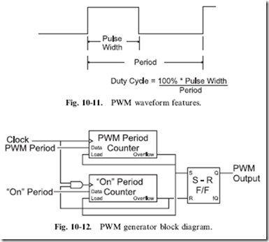
string of timed pulses known as a ‘‘pulse width modulated’’ (‘‘PWM’’) signal (Fig. 10-11). A PWM signal is a repeating signal that is ‘‘on’’ for a set period of time that is proportional to the voltage being output. I call the ‘‘on time’’ the ‘‘pulse width’’ in Fig. 10-11 and the ‘‘duty cycle’’ is the percentage of time the ‘‘on time’’ is relative to the PWM signal’s ‘‘period’’.

To output a PWM signal, there are several possible methods. One way is to use two counters that have a common clock. When one counter overflows, it resets itself and the second counter. Until the second counter overflows, the output of the circuit is set to ‘‘1’’. When the second counter overflows, the output of the circuit is reset until the first counter overflows and the process is repeated. Figure 10-12 shows how this type of circuit could be implemented.

This PWM generator circuit uses counters that are reloaded (from the ‘‘Data’’ pins) upon an ‘‘Overflow’’ positive pulse. The ‘‘PWM Period Counter’’ (the ‘‘first counter’’) runs continuously and when it overflows (reaches the final count), it resets and reloads the count value for not only itself but also for the second counter (the ‘ ‘‘ On’’ Period Counter’).

When the PWM Period Counter resets, it ‘‘Sets’’ the S-R flip flop, driving the ‘‘PWM Output’’ high for the start of the PWM signal output. The ‘‘On’’ Period Counter is reset and reloaded by the PWM Period Counter and runs until it overflows. When the ‘‘On’’ Period Counter Overflows, the PWM

image

Output is halted and it also stops running until the PWM Period Counter reloads it, which resets the ‘‘Overflow’’ output and allows the Counter to drive the ‘‘On’’ Period Counter once more.

Another type of PWM generator is shown in Fig. 10-13. The counter output will be continuously compared against a bit value and when the bit value is greater than the counter value, a ‘‘1’’ will be output. The block diagram for the circuit that I envisioned is shown in Fig. 10-13 and can be built quite easily as I show in this section.

When you study Fig. 10-13, there will probably be one point that won’t make sense to you: I show that the counter ranges from 0 to 14 and not 0 to 15, as you would expect for the typical four-bit counter. I wanted the counter to reset itself at 14 rather than 15 so that when the binary values were compared, a 100% duty cycle could be produced as well as a 0% duty cycle by outputting a ‘‘1’’ when the set value was greater than the counter value. If the counter ran from 0 to 15 then the circuit would not be able to produce a PWM with a 100% duty cycle.

To produce the bit range from 0 to 14, I used the 74 x 191 chip counting down and tying the ‘‘_LOAD’’ pin to the ‘‘_RIPPLE’’ pin and driving the inputs to 14. The ‘‘_R’’ (‘‘Ripple’’ Output) pin becomes active when the chip is ‘‘rolling over’’ from one extreme to another and the ‘‘_LD’’ pin moves the value at the input pins into the counter’s latches when it is active. Normally, when a four-bit counter is ‘‘rolling over’’ as it counts down it goes from 0 to 15, but by tying the ‘‘_R’’ pin to the ‘‘_LD’’ (negative active ‘‘Load’’) pin of the 74 x 191, you can load in a new value when the counter reaches 0 and is about to roll over. This feature is ideal for this application as it ensures the count stays in the range of 0 to 14.

image

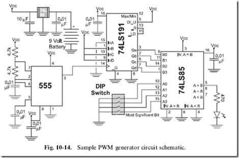
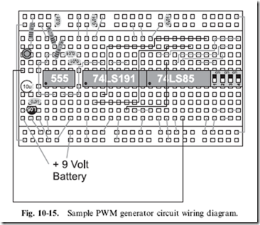
Converting the block diagram to a schematic one is very straightforward (Fig. 10-14) and wiring it onto the PCB’s breadboard is tight but not really a challenge (Fig. 10-15). The PWM output value is specified by the four- position DIP switch. I placed 0.01 mF decoupling capacitors on all of the power inputs of each of the chips. These decoupling capacitors are very important when working with the standard (not CMOS) 555 because it can place large transients on the power line.

I used TTL chips (powered by 5 volts from the 78L05 regulator) rather than CMOS chips because I found that it is difficult locating 74C85 chips.

An advantage of using TTL instead of CMOS for this circuit was that I could simply pull the comparator inputs to ground without the need of a pull up resistor. If you build this circuit with CMOS chips, make sure that you have 10 k pull up resistors on the DIP switch to ensure a high voltage is passed to the comparator.

Once you have built the circuit, you will find that the LED’s brightness will be dependent on the value on the DIP switch. It will be confusing, as the value on the DIP switch will seem to be the opposite to the behavior of the PWM. When all the switches are ‘‘on’’, the LED will be off and, for what seems to be a ‘‘large’’ value, the LED will be dim. When all the switches are ‘‘off’’ the LED will be full on. This confusion is a result of the ‘‘on’’ marking indicating when the switches are closed, not when the signal is a ‘‘1’’ or ‘‘high’’ (which is often extrapolated to being ‘‘on’’) – when the switches

image

are closed (‘‘on’’), the comparator input is pulled to ground and has the value ‘‘0’’.

For all PWM circuits (not just the two I’ve shown here), you must remember that the effective frequency is the input clock frequency divided by the counter value. For the example circuit shown here, the 10 kHz signal is divided by 15 (how many cycles the 74LS191 counts before resetting) so the resulting output signal frequency is 667 Hz, which is still faster than the human eye can perceive a flashing LED, but much lower than required for some DC motors. PWMs are commonly used to control the speed of electric motors and if the PWM frequency is within the audible range of human hearing, you will hear a definite ‘‘whine’’ from the motors. The solution to this problem is to either run the PWM at frequencies above human hearing (greater than 18 kHz) or below the range of human hearing (60 Hz or below).

The lower PWM frequencies should not be an issue to produce, but the higher ones can be a challenge, especially if more bits are used in the counter.

For example, to create a 20 kHz PWM output signal, you will have to provide a 300 kHz clock for a 15-value PWM and 5.1 MHz for a 255-value PWM! You may find that to get a practical circuit, you will have to find a compromise between the number of bits used in the PWM for the signal level and the speed of the oscillator that is going to be used with it.

An interesting feature of a PWM is how it can save you power. If you were to run the PWM with a 75% duty cycle, what do you think the average power output would be? If you answered 75%, then you didn’t go back in the book to look up the power formula. Power is defined by the formula:

P = V x i

and substituting in values from Ohm’s law, it can be also expressed as:

image

From these formulas, it should be obvious that if the voltage is high only three-quarters of the time, the power dissipated by the device being driven by the PWM is nine-sixteenths or 56% of the total power used by PWMs running with a 100% duty cycle. This means that, along with providing the ability to ‘‘throttle’’ direct current devices, a PWM can also result in significant power savings as well.

Finally, you might be confused that I gave you two quite different implementations of the PWM circuit; I did this to show you that there is almost always more than one solution to any problem. I normally recommend that new designers come up with three solutions to a problem before going ahead and implementing something. Having three solutions to choose from will allow you to compare features and drawbacks and choose the solution that is best for the application.

Button ‘‘Debouncing’’

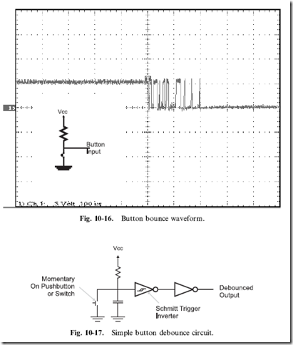
I consider the issue of debouncing switches and buttons to be one of the most important and vexing problems that you will have to deal with when you are developing applications that work with operator input. Most people think that electrical connections happen instantaneously; you might be surprised to discover that the contacts within a switch actually bounce a few times before the switch makes a constant contact. This is shown in the oscilloscope picture in Fig. 10-16.

Earlier in the book, I showed you a simple method of debouncing a switch input by creating a small memory device from two inverters. A major drawback of this circuit is that it ‘‘backdrives’’ the outputs of one of the inverters, but this problem can be eliminated through the use of CMOS inverters and a 10 k current limiting resistor. Even with this fix in place, there is another problem to consider when deciding whether or not to use this circuit – finding double throw push buttons can be difficult. This circuit is well suited for double throw switches but, from the practical difficulty of finding double throw buttons, it becomes impractical.

image

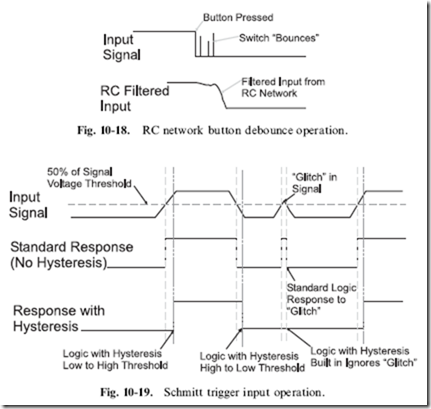
The debounce circuit that I recommend you use is shown in Fig. 10-17. This circuit consists of a resistor–capacitor network that charges over a given amount of time or discharges quickly through a closed switch or button. Figure 10-18 shows the filtering of the bouncing; it is not perfect, but it is much better than what we started with.

The inverter with the funny symbol in Fig. 10-17 is called a ‘‘Schmitt Trigger Input Inverter’’ and provides an extra measure of filtering of the button input. Schmitt trigger inputs are designed to change state on the rising or falling edge of a signal with ‘‘hysteresis’’, as shown in Fig. 10-19.

image

‘‘Hysteresis’’ is the property of the Schmitt trigger inputs in which the threshold point for the rising edge of the signal is different than the falling edge. Looking at Fig. 10-19, you can see that the rising edge threshold is above the ‘‘normal gate voltage threshold’’, while the falling edge threshold is less.

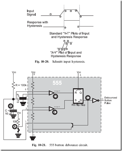
These changing threshold values are the reason for the strange symbol on the inverters, indicating Schmitt trigger inputs. Figure 10.20 shows the input versus the gate response on an ‘‘X-Y’’ chart. The ‘‘X’’ axis is the input voltage with rising voltages to the right and the ‘‘Y’’ axis represents the response of the Schmitt trigger input. By following the numbers, you can see the response of the input and that it forms the same symbol that I put on the inverter gates. For comparison, a traditional logic gate does not use this symbol – the response threshold is the same for rising and falling edge signals.

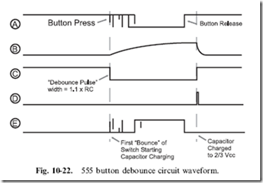
Another method of debouncing button inputs is to use a 555 or monostable circuit. In Fig. 10-21, I show a 555 wired as a monostable, driving out a pulse from a button press. The internal waveforms of the circuit

image

are shown in Fig. 10-22, which shows that any subsequent bouncing of the button after it makes its first connection are ignored by the circuit as the pulse is being output. If you work out the pulse time from R and C, you’ll discover that the pulse time is roughly 1 second in length. This should be long enough for a single button press to be registered and the user to remove his fingers. Obviously, this delay is too long to implement multiple buttons or even any kind of data entry functions in the circuit. To do this, you should consider the next section.

image

Switch Matrix Keypad Interfacing

As I ended off the previous section, you cannot use simple button debouncing techniques to implement a large number of buttons or even a keyboard for data entry. Just so there’s no confusion, I consider a ‘‘large number of buttons’’ to be four or more; providing individual debounce circuits for anything more than a couple of buttons is expensive and time consuming. Along with the cost and time involved, you will also have to come up with some way of prioritizing the button inputs and recognizing non-standard keys like ‘‘shift’’ and ‘‘control’’.

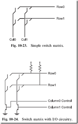
The keys and buttons in PC keyboards and numeric keypads are arranged in ‘‘rows’’ and ‘‘columns’’ and they can be drawn out in such a way that they look like a ‘‘matrix’’. A ‘‘momentary on’’ switch is placed at the intersection of each row and column, as shown in Fig. 10-23. This ‘‘switch matrix’’ provides the ability to ‘‘scan’’ a large number of button inputs with a relatively small number of lines. Your PC’s 104/105 keyboard usually has a 22 by 7 matrix connection to a microcontroller, which scans through the keys and reports any key presses using the algorithms presented in this section.

Keyboards with a 100 keys or more are an extension of the four-button key matrix shown in Fig. 10-23 and have the same concerns and issues to watch out for.

You probably cannot see immediately how the individual keys or buttons of the switch matrix shown in Fig. 10-23 can be polled, but the operation will probably become clearer when you see the resistors and transistors I’ve added to the switch matrix in Fig. 10-24.

image

In this case, by connecting one of the columns to ground, if a switch is closed, the pull down on the row will connect the line to ground. When the row is polled by an I/O pin, a ‘‘0’’ or low voltage will be returned instead of a ‘‘1’’ (which is what will be returned if the switch in the row that is connected to the ground is open due to the pull up on it). To scan the keyboard, the column transistors are turned on, one at a time, and while the column transistor is on and the column is pulled to ground, the rows are compared to a logic level of ‘‘0’’, which would indicate that the button is pressed.

This methodology for handling switch matrix keypad scans I’ve outlined here probably seems pretty simple. Depending on your familiarity with programming and different microprocessors and microcontrollers, you will probably realize that implementing these functions could be done even simply in assembly language programming or ‘‘C’’. You should also realize that this code would be quite difficult to implement just using logic chips.

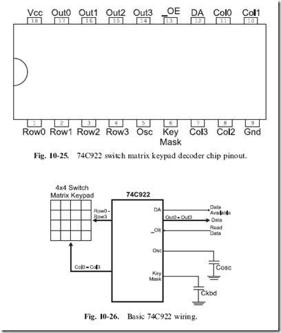
To avoid the complexities of trying to develop TTL logic that will carry out the functions described in the pseudo-code presented above, I normally

image

use the 74C922 keypad decoder chip (Fig. 10-25). This chip can be used to debounce and encode up to 32 buttons (although 16 is the normal maximum) and carries out button debouncing internally as well as keeping track of two currently held-down keys when new keys are pressed. The 74C922 is quite easy to wire to a four by four (16 button) switch matrix keypad, as shown in Fig. 10-26. By ‘‘doubling up’’ rows of sensors of the 74C922, you can add a number of additional keys to the application. In the next section, I will show how this is done to create a 20 button input device (with up to 32 possible).

The two capacitors are used to create a relaxation oscillator within the chip that is used to ‘‘scan’’ through the buttons as well as provide a ‘‘debounce’’ delay count for the application. The two capacitor values are calculated as:

image

I like a debounce interval of 20 ms: plugging this into the formulas above, I get a value of 2 mF and 20 mF. When I build my own applications, I tend to have a lot of 10 mF (for power filtering) and 1 mF (for MAX232 RS-232 level converters) electrolytic capacitors on hand. I have not found any problems with using these components and I would recommend that you use them as well to avoid having to stock multiple capacitor values for different applications.

Quiz

1. What are ideal sequential circuit interfaces?

(a) LCDs

(b) Individual switches and LEDs

(c) Keyboards

(d) USB flash disks

2. What is the suggested digital electronics interface to an Hitachi 44780 controlled LCD display?

(a) Hardware state machine

(b) Microcontroller

(c) Sequential circuit

(d) Combinatorial circuit

3. Is a bus ‘‘Read’’ or ‘‘Write’’ faster?

(a) Write is faster

(b) Read is faster

(c) Using a synchronous clocked circuit, they take the same amount of time

(d) Read is slower due to the need to retrieve data from the inter- face device

4. Seven-segment LED displays have a common:

(a) LED anode or cathode

(b) Segment pins

(c) LED drivers built into the package

(d) Pin interface that is used by all devices, regardless of the number of digits in the package

5. Multiple seven-segment LED displays show different values by using:

(a) Linear feedback shift registers that have encoded the bit patterns

(b) Turning on each individual digit with its unique value periodically

(c) Multiple LED driver circuits that drive the value for its respective digit to the LED display

(d) Multiple bits of memory, one for each segment, which are loaded according to the display value

6. For a PWM circuit running its logic at 5 volts and a duty cycle of 67%, what is the ‘‘on’’ voltage level of the output signal?

(a) 0.67 volts

(b) 5 volts

(c) 2/3 volts

(d) 3.35 volts

7. The power dissipated by a PWM running with a 20% duty cycle will be what fraction of a 100% duty cycle?

(a)

0.04

(b)

40%

(c)

0.4

(d)

400%

8. A 555 monostable with R ¼ 100 k and C of 4.7 mF will output a pulse of:

(a) Approximately 0.5 s

(b) Approximately 4.7 s

(c) Approximately 1.1 s

(d) Insufficient data given to determine the pulse width

9. Rows and columns in a switch matrix keypad have what connected to them?

(a) The rows have a transistor connected to ground and the columns have a capacitor

(b) The columns have transistors connected to ground and the rows are left open

(c) The columns are left open and the rows have a transistor connected to ground

(d) The columns have transistors connected to ground and the rows have pull up resistors

10. The 74C922 reads a switch matrix keypad by:

(a) Pulling the columns of a switch matrix keypad to ground and scanning the rows for pulled down bits

(b) Driving a 1 kHz square wave on the rows and polling the

columns for the signal

(c) Using an internal microprocessor

(d) Measuring the capacitances of individual lines and looking for changes


Circuit Interfaces :Address and Data Decoders and Multi-Segment LEDs

Circuit Interfaces

For a sequential digital electronic circuit to be effective, it has to interface with something. This something could be a person or it could be other digital electronic circuits. If you were to look at different interfaces for either case (human or machine), you will discover that as the function of the circuit increases in sophistication, so does the interface. The reasons for this increase in interface complexity can be attributed to an increased amount of data to present as well as an increased number of operating parameters to choose from and select. The challenge is to come up with a way of adding these user and device interfaces simply, effectively and not affect the operation of the central sequential circuit.
Simple logic level switches and individual LEDs for each bit are perfect examples of the types of interfaces that I am talking about; to add these devices to your application, you generally don’t require any types of busses nor do you need to have any special communications protocols for communicating with the devices. These interfaces are simple to add and modify to an application.

The problem with simple logic level switches and LEDs connected to each bit is that they cannot be very descriptive; nor are they very efficient methods of transferring data. An eight bit system is quite manageable, but it becomes

very difficult when there are tens, hundreds or even thousands of bits to control and monitor. Early computers started out using simple switches and lights for input and output, respectively, but quickly outgrew them and began using printers, teletypes and punch cards to get state information from the computer. Today’s computer systems have very sophisticated input and output capabilities, requiring the power of a processor that would have been identified as a ‘‘supercomputer’’ 10 years ago or less.
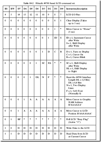
An example of a complex interface that you would be hard pressed (if it were possible at all) to create digital electronics for is the Hitachi 44780 based LCD module (Fig. 10-1). The controller hardware is fairly complex and must be accurately timed. The LCD module works like a ‘‘teletype’’ or a single line TV display – as you write characters to it, a ‘‘cursor’’ will move to the right, to prepare for the next character. The character interface consists of the eight data bits and three I/O pins listed in Table 10-1.

clip_image003

Fig. 10-1. Sample LCD output.

image

image

I typically attach a series of pins to the 14 connector pins so that the LCD can be easily mounted on a breadboard. In some LCDs, you may discover that there are 16 connector holes with the extra two holes used for backlighting. Some other LCD modules have two rows of seven or eight pins. For the ease of creating the experiments in this book and wiring them to the breadboard you should just use LCD modules that have a single row of pins.

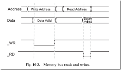
Wiring the LCD to the hardware is quite straightforward as you will see in the waveform diagram (Fig. 10-2). The only unexpected aspect of the interface circuit is a potentiometer used to set the ‘‘contrast voltage’’ used by the LCD. The potentiometer is wired as a voltage divider, with the contrast voltage pin connected to the wiper of the potentiometer. Depending on the type of LCD that you are using, you will find that the voltage producing the best contrast will either be high or low, depending on the technology used in the LCD.

To communicate with the LCD, you will have to send the data word slisted in Table 10-2 via the LCD interface. These bytes are commands that set the operating mode of the LCD or command it to perform some other operation. In Table 10-2, I have listed the different commands, along with the ‘‘RS’’ and ‘‘RW’’ lines that are used to control them. To clock in the command, the ‘‘E’’ bit must have a high value (‘‘1’’) written to it and then a low value (‘‘0’’).

Data displayed on the LCD is, for the most part, ASCII and you can pass ASCII characters directly from the hardware to the LCD. I say that the LCD can display ASCII ‘‘for the most part’’ because you will find that some characters are not supported (such as the backslash, ‘‘’’) and if you go outside the normal ASCII character limits, you will see Japanese characters on the display. If you were to send a carriage return, line feed or any of the other ASCII terminal command characters, you would discover that they Table 10-2 Hitachi 44780 based LCD command set.
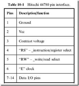
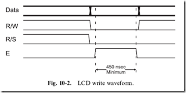
image

result in a strange character being displayed. If you want to provide more ‘‘terminal’’-like functions to the 44780 based LCD you will have to write them yourself and add them to your application.

Most commands execute in 160 ms or less with the display clear and move cursor to home commands can take up to 5 ms. The initialization process for the LCD is:

1. Wait more than 15 ms after power is applied.

2. Write 0x030 to LCD and wait 5 ms for the instruction to complete.

3. Write 0x030 to LCD and wait 160 ms for instruction to complete.

4. Write 0x030 AGAIN to LCD and wait 160 ms or Poll the Busy Flag.

5. Set the Operating Characteristics of the LCD:

● Write ‘‘Set Interface Length’’

● Write 0x010 to disable display shifting

● Write 0x001 to clear the display

● Write ‘‘Set Cursor Move Direction’’ setting cursor behavior bits

● Write ‘‘Enable Display/Cursor’’ & ‘‘Enable display and optional cursor’’.

The LCD could be controlled by a state machine, but there would be a significant amount of work to do this (and the state machine would be quite large). Along with the eight bit interface, the LCD can also be controlled by a four bit interface; each character and eight bit instruction is passed in four bit blocks through the D7:4 pins, but this interface would probably be even more difficult to create for the LCD module.

Address and Data Decoders

When you have decided upon the interfaces to your application, you will probably have to determine the best method of selecting which device is active at any time. The method that would make the most sense is to use the same method that a microprocessor uses: output a bit value, selecting the device and one control bit to activate the interface device. Depending on the resources available, the section bits may consist of a number of bits, each one passed to a different interface device, or a binary value, which is decoded into a specific control bit.

image

Ideally, the signal being passed to the interface device would look something like Fig. 10-3 – an ‘‘Address’’ value is passed to the device and after a data ‘‘set up’’ time, a Read (‘‘_RD’’) or Write (‘‘_WR’’) line becomes active. A ‘‘Read’’ action polls the interface device and returns the value to the sequential circuit. A ‘‘Write’’ action does the exact opposite: it sends a value from the sequential circuit to the interface device.

You should notice that the timing of the read and write operations are quite a bit different. The short ‘‘Read’’ pulse is indicative of the expected operation of the device being accessed; once it receives the ‘‘Read Address’’ which selects the device, it takes some time to prepare the data before it can be read out. Similarly, when writing data, the _WR line is active for a surprisingly long period of time to allow the interface device to pass the data internally and prepare the interface circuitry to correctly store the data.

The interface read and write operations are good examples of situations where the latches rather than registers are used. When the _RD and _WR signals become active, data should be passed through them as quickly as possible rather than being held on a rising or falling value of the signal edge. For most applications, this need for taking advantage of every possible picosecond of time for data transfer is not needed, but you will find that it’s a good idea to work with a standard design interface that will work in all

situations.

Following this philosophy, rather than providing an individual bit to each interface device, how about a binary ‘‘address’’ that can be decoded to an individual address using a ‘‘decoder’’ like the 74139 (Fig. 10-4) that converts a two bit value into four individual active low outputs. The 74139 contains

image

two ‘‘two to four’’ decoders like the ones shown in Fig. 10-5. Decoders (also known as ‘‘demultiplexors’’) convert binary values into individual output lines and are primarily used to decode memory addresses to individual chips.

The resulting ‘‘interface’’ is essentially a computer ‘‘bus’’ and will allow you to add standard computer interfaces to your circuit, probably with no modification. You might have been wondering why I went through the effort of providing an interface select function along with the _RD and _WR signals – you may be thinking that a single pin that both selects the device as well as initiate the read or write would be enough; the philosophy of interfacing like in a computer is only so useful. This is true if you are going to only work with custom-designed interfaces, but there are a lot of standard interfaces (including the various ones presented in this chapter) designed for being accessed by computer systems that you will want to take advantage of.

Multi-Segment LEDs

I think you would be hard pressed to find somebody in the industrialized world that has never seen a ‘‘seven-segment’’ LED display (Fig. 10-6) before. It first became popular in the 1970s and is used in almost literally everything from digital clocks to car instruments. Seven-segment LEDs can be found virtually everywhere, being used not only in digital watches but also in kitchen appliances, cars, instruments and, of course, in videocassette recorders (VCRs). The flashing ‘‘12:00’’ on a clock or VCR created using seven-segment LEDs is the symbol of a person’s inability to handle the latest in technology.

In Fig. 10-6, I have shown the appearance of the seven-segment LED display – it can be put in the same ‘‘footprint’’ as a 0.300 inch’’ wide 14 pin DIP package, but some of the pins (‘‘N/C’’ for ‘‘no connect’’) are not present. The ‘‘DP’’ LED stands for the ‘‘decimal point’’.

The seven-segment LED display can be wired as either a ‘‘common anode’’ or ‘‘common ‘‘cathode’’; in this experiment we will be using ‘‘common anode’’, wired as shown in Fig. 10-7. For this part, the two ‘‘common’’ pins are connected to all (and occasionally some) of the anodes of the eight LEDs built into the display. This simplifies the wiring you will have to do somewhat and makes working with multiple displays a bit easier, as I will show in a later experiment.

Despite its commonality, the seven-segment LED display is not trivial to work with. There are a number of chips on the market that make the component easier to work with in some applications, but when you are working with your own sequential circuits, you will find that these ‘‘canned’’ functions never quite do what you hope for.

image

image

As you are probably aware, by turning on each of the different LEDs with their unique values individually, you can create a multiple-digit display. Figure 10.8 shows how by turning on different LED segments, the display can be used to display the 10 numeric characters. Along with the 10 numbers, there are a number of letters that can be displayed, although only a few of them look exactly like the characters they are supposed to represent. If you want to display letters as well as numbers, then you will have to use a LED with more segments – these are available as either 16-segment displays or as matrixes of LEDs that display the character as a multi-dot ‘‘font’’ like on your computer screen.

Each LED in the display can be wired conventionally to control whether or not they are turned on or off. Controlling individual LEDs in a single display is quite easy. It gets quite a bit more difficult when you have to display different values on multiple LED displays. To convert incoming bits to meaningful characters on the display, you will have to pass the bit values through a combinatorial circuit, like the one shown in Table 10-3 for the first four decimal digits.

In Table 10-3 in the ‘‘Comments’’ column, you can see that I have noted any commonalities between different equations and noted that segment ‘‘B’’

is always active for all four digits. I should point out that coming up with the equations for each of the segments is good practice for working with Boolean arithmetic equations, but it is much easier and simpler to buy a seven- segment LED driver. The 7447 chip is commonly used for decoding the incoming bits and driving the LEDs and is an excellent solution when there is

image

only one seven-segment LED display outputting information from the application.When multiple LED displays are required, instead of providing multiple- digit drivers, a single-digit driver is used and different values are passed to it for different displays very quickly. Figure 10-9 shows a four-digit LED display with each digit having a different value. Each digit is turned on momentarily to display its value and then switched off for the next digit. The eye’s visual persistence ignores the flickering if the sequencing is done fast

image

enough and it appears that all the digits are on simultaneously, even though they are displaying different values.

As a rule of thumb, each display should be active 50 or more times per second. The slower each display is flashed on and off, the more likely the human eye will pick up the flashing. A flashing multi-character display is not attractive and could cause headaches in some people (especially if the displays are very bright). The time each display is turned on must be as equal as possible. If one display is on for a longer period of time than the others, then it will appear brighter and, conversely, a display active for a shorter period of time will appear dimmer. When working with multiple displays, in order to meet the 50 times per second guideline, you are actually going to have to loop through your individual display action 50 times per second multiplied by the number of displays. So, for a four-digit display, you will have to loop 200 times per second and each digit will be on for 5 ms at a time. There are some chips, such as the very popular Maxim MAX7219 (Fig. 10-10), which can control multiple seven-segment LED displays. This chip takes care of all the driving and timing requirements for the displays; the only catch is that you must shift in the desired value for the display.


Complex Sequential Circuits:Linear Feedback Shift Registers and Hardware State Machines

Linear Feedback Shift Registers

One of the most interesting logic devices you can work with is the ‘‘linear feedback shift register’’ (‘‘LFSR’’). It is built from a shift register along with two or more XOR gates modifying the contents of the register as shown in Fig. 9-12. This circuit can be used to ‘‘pseudo-randomize’’ data, encrypt and

image

decrypt serial data and provide very good serial data integrity checking. You may have heard the term ‘‘cyclical redundancy check (‘‘CRC’’) when applied to data transmission; this is a type of linear feedback shift register. Linear feedback shift registers can also be implemented fairly easily in software with a microcontroller or microprocessor, although it is in hardware where the device is the most efficient.

The simple LFSR illustrated in Fig. 9-12 feeds back bits 5 and 7 of the shift register through XOR gates to the input. This changes the bit values in the shift register according to the formula:

imageThe LFSR is typically used for three purposes:

1. Creating a ‘‘checksum’’ value known as a cyclical redundancy check (CRC), which is a unique value or ‘‘signature’’ for a string of bits. Both the transmitter and receiver will pass the data through LFSRs and, at the end of the process, the CRC produced by the transmitter will be compared to the CRC produced by the receiver. If there is a difference in the CRCs, then the receiver will request that the transmitter resend the data.

2. Encrypting a string of bits. LFSRs can be used as an encryption/ decryption tool with part of the encryption being the initial value in the LFSR. The value output from the LFSR is dependent on the initial value loaded into the LFSR. Decrypting data is also accomplished by using an LFSR, but configured as the complementary function.

3. Producing ‘‘pseudo-random’’ numbers. One of the most challenging computer tasks that you will be given is to come up with a series of random numbers. Computers are designed to be ‘‘deterministic’’, which means that what they are doing at any given time can be calculated mathematically. This property is important for most applications (nobody wants a computer to boot differently each time or to have a word processing program that responds randomly to keystrokes), but it is a problem for many applications which rely on the pseudo-random numbers for animated displays or ‘‘lifelike’’ responses to user input.

image

In all of these applications, the LFSR is an ideal choice as a solution because it can be built very simply from just a few gates (meaning low cost and fast operation). The LFSR can also be implemented in software, as I will show below.

If you were going to express this LFSR to somebody else, you could send a graphic something like Fig. 9-13, or you could express it in the ‘‘polynomial’’ format like:

image

The polynomial format is the traditional way of expressing how an LFSR works and is used by mathematicians to evaluate an LFSR operation.

There are a few important facts about LFSRs that you should be aware of:

1. The LFSR can never have the value zero in it. If it contains zero, then none of the internal bits will ever become set.

2. The ideal LFSR implementation will be able to produce 2n – 1 different values. It should be obvious that the one value that cannot be produced is zero.

3. A poorly specified LFSR may have the situation where it ends out with a value of zero.

The operation of a single shift of the 8 bit LFSR in Fig. 9-13 can be modeled using the ‘‘C’’ function:

image

image

Hardware State Machines

The hardware state machine circuit was originally designed to allow designers to create a complex application using a simple, single ROM, a few register bits and some basic logic gates instead of a complex sequential circuit design or a processor-based solution. State machines are not widely used in modern applications because the costs of the parts needed to make up the circuit can very easily exceed that of a microcontroller. Almost ironically, hardware state machines are used as the control mechanism for most modern computer systems because they are fairly easy to design, program and debug. The use of hardware state machines (which are typically referred to as just ‘‘state machines’’) as the control mechanism for computer processors has given a new importance to the understanding of state machines.

The typical ‘‘state machine’’ is shown in Fig. 9-14. This circuit consists of an ROM (usually EPROM) which has part of its output data fed back as a ‘‘state address’’. Other address lines are used as circuit inputs and the state machine changes its state address based on these inputs.

image

The clock is used to pass the new address to the ROM and then pass the output from the ROM to the output and input state circuits. The two latches are operated 1808 out of phase to prevent ‘‘glitches’’ from the ROM changing state from invalidly affecting any output circuits. A single edge triggered register is not typically used with the state machine because toggling inputs while the ROM is being accessed could result in invalid data being passed into the latches.

As few output bits are used as the ‘‘state address’’ as possible. The reason for this is to maximize the number of outputs and minimize the number of states which have to be programmed. Each state requires two to the number of inputs to function. Each state responds differently according to the inputs it receives.

A typical application for state machines is a traffic light. If a press-button crossing light, as shown in Fig. 9-15, is considered, a state machine circuit, like that shown in Fig. 9-16 could be used.

image

In normal operation (which is known as ‘‘state 0’’), the green light is on and the button is not pressed. If the button is pressed, then execution jumps to state 1, which turns on the yellow light for 5 seconds (states 2, 3, 4 and 5), after which the red light is put on for 26 seconds (states 6–31). If the button is pressed during states 7–31, then execution jumps to state 6 to reset the timer.

Table 9-1 ROM programming for simple traffic light state machine.

State

Button

New state

Green

Yellow

Red

Comments

B’00000’

1

B’00000’

1

0

0

Power up

B’00000’

0

B’00001’

0

1

0

Power up/button press

B’00001’

x

B’00010’

0

1

0

Yellow LED on

B’00010’

x

B’00011’

0

1

0

Yellow LED on

B’00011’

x

B’00100’

0

1

0

Yellow LED on

B’00100’

x

B’00101’

0

1

0

Yellow LED on

B’00101’

x

B’00110’

0

1

0

Yellow LED on

B’00110’

x

B’00111’

0

1

0

Yellow LED on

B’00111’

x

B’01000’

0

0

1

Red LED on

B’01000’

1

B’01001’

0

0

1

Red LED on

B’01000’

0

B’00111’

0

0

1

Red LED on/reset Ctr

B’01001’

1

B’01010’

0

0

1

Red LED on

B’01001’

0

B’00111’

0

0

1

Red LED on/reset Ctr

.

.

.

.

.

.

B’11111’

1

B’00000’

0

0

1

Return to green

B’11111’

0

B’00111’

0

0

1

Red LED on/reset Ctr

To keep the circuit simple, I want to use an eight bit data bus ROM with six inputs (five state, one button). This means that 2**6 (or 64) states are required in the ROM. These states are listed in Table 9-1. The reset on the input address latch is used to reset the state to 0 on the power up. The button is assumed to be ‘‘pressed’’ if a ‘‘0’’ is returned.

Table 9-1 would then be converted into bits and burned into the ROM. An ‘‘x’’ means both input states have the same result on outputs.

This application is reasonable to code and build, but a problem arises with very complex state machines (ones that require tens of inputs and hundreds of different states). These state machines are normally hard coded into a custom chip rather than built out of discrete parts like I have shown for this application. The reason for placing it within a chip is to give more outputs as well as more states in a custom application. The depth and the width of the data in ‘‘real’’ applications is better suited to custom chips which can have non-custom memories added much more easily than in the situation where only commercial chips are used.

In the example above, I have used a state machine with a one second clock. Obviously in this situation there can be problems (such as the missed input if the button is pressed for less than 1 second and it isn’t released after it is pressed). This function makes state machines unattractive for rapidly changing inputs and any kind of sophisticated real-time processing of inputs is simply not economical to do with the state machine. When I say ‘‘not economical’’, I am thinking in terms of the memory and properly programming the many states.

Quiz

1. In the sequential circuit block diagram where is the clock signal passed to?

(a) To the ‘‘state memory’’ and ‘‘output formatter’’ blocks

(b) To just the ‘‘state memory’’ block

(c) To the ‘‘input formatter’’ block

(d) To the ‘‘reset control circuitry’’ block

2. Asynchronous digital logic design is being pursued because:

(a) It will result in simpler chip designs

(b) Circuitry designed under this philosophy will be easier to interface to

(c) The end of performance gains using traditional design methodologies is in sight

(d) It offers faster operations with less power usage

3. Why are edge triggered registers used for counters instead of latches?

(a) It will result in simpler circuit designs

(b) Circuitry designed under this philosophy will be easier to inter- face to

(c) Less power is required

(d) It offers faster operations with less power usage

4. Ripple counters are:

(a) Always the fastest way to implement counters

(b) Usually more complex electronically than other counter designs

(c) Always the slowest way to implement counters

(d) Similar to ripple adders in operation

5. What are advantages of serial data transmission over parallel data transmission?

(a) Reduced number of drivers and receivers

(b) Faster data transmission

(c) Lower product costs

(d) Higher product quality

6. Where is serial data transmission not used?

(a) The internet

(b) Broadcasting stations to TVs/radios

(c) Keyboard to PC interface

(d) PCI bus interfaces

7. Linear feedback shift registers are built from:

(a) The system architectural drawings

(b) The high-speed circuits to support communications

(c) Shift registers and XOR gates

(d) The basic system serial interface

8. When the value of a linear feedback shift register equals zero:

(a) The operation has completed

(b) Either the initial and input values are zero or there is a problem with the LFSR design

(c) There was an error in encrypting a message

(d) Power has been removed from the circuit

9. Hardware state machines are rarely used except in:

(a) Computer processors

(b) Military and space applications

(c) High-performance custom logic applications

(d) Situations where old ROMs are easily available

10. State machines are normally built:

(a) Out of discrete chips and ROM chips

(b) In complex custom chips

(c) On specially designed carrier PCBs

(d) With the checksum of the ROM printed on them


Complex Sequential Circuits:Counters and Shift Registers

Complex Sequential

Circuits

As the saying goes: ‘‘You now know enough to be dangerous.’’ You should be fairly comfortable with working with logic functions and equations, have an understanding of electronics and how to interface logic chips (of different families together), understand the basics of memory and have gone through a number of clocking schemes. I’m sure that you now feel you are ready to start bringing these pieces together into some interesting applications. I’m sure that you have some ideas of things you would like to have your hand at designing. Before being set free to wreak havoc on an unsuspecting world, I want to spend some time presenting you with some chips and tools that will make your plans for world domination much easier. In this chapter, I want to go through some of the subsystems that are available in chips that will make your design work easier.

In Chapter 7, I introduced you to the digital clock block diagram shown in Fig. 9-1. There shouldn’t be any part of this diagram that is a surprise to you; the ‘‘time memory’’ consists of a number of flip flop registers that are reset

image

upon power up. The ‘‘time update circuit’’ consists of an adder along with logic and a user push button to determine what the next time will be. The ‘‘output formatter’’ consists of logic to decode the time memory and display it on a set of LEDs. Finally, the 1 Hz clock can be produced a number of different ways that are covered in the previous chapter.

While I must admit that it would be cool to see a digital clock designed using two input logic gates, I want to point out that there are a number of commonly available chips that provide major subsystems needed for such an endeavor. For the rest of this book I will be focusing on these chips and how they are interconnected to form ‘‘real world’’ applications.

Virtually all of these chips are sequential circuits in their own right; consider a ‘‘counter’’ chip that increments its internal memory devices each time a rising clock edge is received. The counter chip consists of several flip flop bits and combinatorial logic that processes input data, provides the value increment and outputs the data in a specific format. These functions are very similar to that provided by the digital clock in Fig. 9-1.

To show what I mean, consider the sequential circuit block diagram in Fig. 9-2. Superficially, the diagram has a very strong resemblance to Fig. 9-1 because many of the same basic functions and capabilities are required in both instances.

The ‘‘state memory’’ is the current operating state of the chip. The term ‘‘state’’ simply means at what operating point the chip is at. For a counter or other arithmetic function chip, the term ‘‘state’’ probably seems somewhat grandiose, but it is an accurate way of describing the current value in a counter. For a microprocessor, the term ‘‘state memory’’ is almost an understatement, as it includes not only the program counter (which points to the next instruction to execute) but also data and status register information.

image

The state memory can be reset (as shown in the previous chapter) and, more importantly, it is usually the only point in which the clock/oscillator input is received. The philosophy behind most sequential circuits is that the combinatorial logic processing input, output and the next state information, regardless of the circumstances, will be available in time for the next active clock cycle. The term normally used to describe this methodology of design is ‘‘synchronous’’ because a central clock is keeping track of the operations within the chip.

This philosophy is currently under challenge from scientists interested in investigating ‘‘asynchronous’’ digital logic design. This effort involves designing sequential circuits that are not ‘‘paced’’ by a central clock, but the length of time of each operation. For example, moving data from one register to another should take much less time than an instruction which stores data in the main memory. Asynchronous digital logic design holds the promise of faster computers that use much less power because the only active circuitry are the required gates and flip flops of the current time – nothing else needs to be active, nor do other circuits need to be clocked.

The ‘‘next state update circuit’’ and ‘‘input formatter’’ blocks process the current bit data and any relevant input for storage in the state memory. In Fig. 9-1, I combined both of these functions into the ‘‘time update circuit’’ because the only input required for this clock is whether or not the ‘‘time set button’’ is pressed – if it is, then the time update circuit will increment the hours, minutes and seconds stored in the digital clock’s ‘‘time memory’’.

The ‘‘input formatter’’ circuitry can be processing different inputs controlling what the next state is going to be – this is why I link it to the ‘‘next state update circuit’’. For a counter, this information could be the direction the counter executes in or whether or not the counter counts in binary or BCD.

The output formatter converts data into the required output and provides appropriate drivers for the function. Note that I have drawn a link to this box from the ‘‘reset control circuitry’’ despite my statement earlier that only the state memory could be reset. The reason for drawing in this link is to indicate that the chip may have tri-state drivers and these are held in a high impedance (‘‘off ’’) condition while reset is active.

As you work through the material in the rest of the book, try to see how the described chip functions fit in with this model. You might have a better model to work with that makes more sense to you and if this is the case use it. The model that’s presented here allows me to visualize what is happening in an application, and it would be arrogant of me to assume that it works for everyone else.

Counters

One of the most useful functions that you will use when you develop digital electronic circuits is the counter. The counter is actually a smaller piece of many complex chips, as it provides a basic way of maintaining the current operating state along with a method of progressing to the next one. The basic counter circuit consists of a set of flip flops that drive into and are driven from an adder. A counter circuit is shown in Fig. 9-3. The use of ‘‘edge triggered’’ flip flops is a very important aspect of the circuit shown in Fig. 9-3 and one that you should keep in mind. When the ‘‘counter clock’’ changes state, the output value of the adder (which is the D flip flop value plus 1) is presented to the inputs of the D flip flop register bits as the next value to be saved.

image


image

If an edge triggered flip flop register wasn’t used in the circuit, then you would have to use latches and design the counter something like the one shown in Fig. 9-4. In this circuit, I have put in two latches, each one ‘‘out of phase’’ with each other. This is to say that when the clock is high, one latch is storing the data while the other is passing through the value presented at its inputs. When the clock changes value, the latches change from passing data to storing and vice versa. This method of implementing a counter is unnecessarily complex and potentially very slow – the extra set of flip flops will slow down the performance of the counter and limit its maximum speed.

The counter circuit of Fig. 9-3 can be built using a 74C174 hex D flip flop and a 74C283 four bit adder circuit. The circuit shown in Fig. 9-5 will demonstrate how the counter works. When the term ‘‘floating’’ is used with respect to pins, it means that the pins are left unconnected.

When you try out this circuit, the first thing that you will probably notice is that when you press the button, the LEDs will not ‘‘increment’’ by 1, but by 2, 3 or even 4. The reason for this is known as ‘‘switch bounce’’. Earlier in the book, I showed a two inverter circuit for eliminating switch bounce, and later I will discuss a number of other strategies for minimizing the problem. For now, if you wire a 0.1 f,LF tantalum capacitor as shown in Fig. 9-5, you should minimize this problem (although you will probably not eliminate it).

The counter circuit should work well for you. As with the previous projects, a single chip can be used where multiple required. The counter chip that I usually work with is the 74LS193 (Fig. 9-6) which combines a four bit D flip flop register and adder along with the ability to decrement the result. Later in the book, I will show how this chip can be used with others to ‘‘cascade’’ from a 4 bit counter to an 8 and 16 bit counter.

image

The ‘‘_Carry’’ out bit of the 74193 can be passed from one counter to the clock input of another to provide the ability to count more bits, as I show in Fig. 9-7. The carry bit can be thought of as an overflow to the more significant counter, indicating that it should increment its value. If by looking at this circuit you recognize it as being similar to the ‘‘ripple’’ adder presented earlier

image

in the book, go to the head of the class. This circuit is known as a ‘‘ripple counter’’ and does not have the same high speed as a counter built from look- ahead carry adders.

Along with the 74193, you might want to consider the 74161 counter,

which can only count up and changes to the count value must be clocked in (the 74193 allows changes to the count value asynchronously, which is to say without the clock). The 74160 and 74192 chips are identical to the 74161 and 74193, respectively, but only count up to 9 and are known as ‘‘decade’’ counters. The 74160 and 74192 are useful in circuits in which the digits 0 through 9 are required for counting.

Shift Registers

Most intersystem (or intercomputer) communications are done serially. This means that a byte of data is sent over a single wire, one bit at a time, with the timing coordinated between the sender and the receiver. So far in this book, if you were to transfer a number of bits at the same time, you would send them in ‘‘parallel’’, one connection for each bit. The basis for serial communications is the ‘‘shift register’’, which converts a number of ‘‘parallel’’ bits into a time-dependent single string of bits and converts these strings of bits back

image

into a set of parallel bits. Figure 9-8 shows this process with eight parallel data bits being converted into a bit stream and transmitted to a receiver, which ‘‘recreates’’ the eight bits back into their parallel data format.

The differences between serial and parallel data transfers are shown in Fig. 9-9. To send six bits in parallel, a half dozen transmitting ‘‘drivers’’ and an equal number of ‘‘receivers’’ are required. To send six bits serially, just a single driver and receiver is required, but the sending circuit must have a ‘‘shift register transmitter’’ and the receiving circuit must have a ‘‘shift register receiver’’. The parallel data can be sent in the time required for just one bit while the serial data requires enough time to send each of the six bits individually.

It probably looks like transmitting data serially requires a lot of overhead and it slows down the data transfer. There are a number of factors to consider before making this assumption. The first is that most chips are not made out of individual logic gates as the simple chips presented here so far; they are

image

usually very dense circuits consisting of thousands of gates, with the impact of adding serial shift registers being very minimal. Another issue to consider is that it can be very difficult to synchronize all the parallel bits to ‘‘arrive’’ at the receiver at the same time in high-speed circuits. Finally, multiple wires can take up a lot of space and be quite expensive; if chips or subsystems could have shift registers built into them, then it often makes sense (both practical and economic) that data be transferred serially.

The circuit that converts the parallel data into the serial stream is quite simple. Figure 9-10 shows a circuit along with a waveform showing how the circuit works. Four bits are first loaded in parallel into a series of four flip flops. These four flip flops can be driven with data either from an external source or from the next significant bit depending on the ‘‘Ctrl’’ bit state. If ‘‘Ctrl’’ is high, when the ‘‘Clk’’ (‘‘clock’’) is cycled, the data in the D3:0 bits are stored in the four flip flops. If ‘‘Ctrl’’ is low, when ‘‘Clk’’ is cycled, each bit is updated with its next significant bit and data is shifted out, least significant bit first.

The process of each bit of data ‘‘passing’’ through each of the flip flops is known as ‘‘shifting’’. As can be seen in Fig. 9-10 that four data bits are ‘‘shifted’’ out on the ‘‘Sdata’’ line in ascending order, with the ‘‘Clk’’ line specifying when a new bit is to be shifted out. If this method was used to

image

transmit data between two digital devices, it would be known as ‘‘synchronous serial data transmission’’.

Receiving ‘‘Sdata’’ is accomplished by simply using four flip flops wired with their outputs wired to the next input, as I’ve shown in Fig. 9-11. The same clock that is used to shift out the data from the transmitter should be used to shift in the data in the receiver. Along with the circuit used to shift in the data, I have included a waveform diagram for you to take a look at in Fig. 9-11. One potentially confusing aspect of the waveforms is my use of the ‘‘DoX’’ convention to indicate the previous values within the receiver. These bits will be shifted out in a similar manner as to how the data was shifted in.

There are a number of very common synchronous data protocols that are used in computer systems to provide simple interfaces to common peripherals. These interfaces, which include ‘‘Microwire’’, ‘‘SPI’’ and ‘‘I2C’’, are very easy and relatively fast ways of adding peripherals such as analog to digital converters and external memory to microcontrollers and complete computer systems. In fact, your PC has an I2C processor peripheral bus for controlling power supplies and monitoring the processor’s chip temperature.


Oscillators:Crystals and Ceramic Resonators,555 Timer Chip and Delay Circuits

Crystals and Ceramic Resonators

For the best clock accuracy, a quartz crystal should be used in an oscillator circuit like the one shown in Fig. 8-13. A quartz crystal is a piezoelectric device that provides a constant delay between one side of the piece of quartz within the part to the other. The term piezoelectric refers to the property of quartz (and some other compounds) to mechanically deform when a current is applied to it or produce a voltage potential when it is mechanically deformed.

In an oscillator, the quartz crystal will have a voltage applied to one end of it and this will cause the quartz crystal to deform. The rate at which this deformation takes place is known and will cause a voltage potential to be produced at the other end of the quartz crystal after a known delay. This voltage is used as a feedback value to an inverter built into the oscillator circuit. The NPN bipolar transistor-based inverter can be seen in Fig. 8-13.

The circuit in Fig. 8-13 is somewhat ‘‘fiddly’’ to build and to get working reliably. There are some formulas that can be used to specify the different resistor, capacitor and inductor values, but, personally, I would never use this circuit in my own applications. This is why I did not put in any component values on the diagram; instead, I would use the inverter-based oscillator shown in Fig. 8-14. In this circuit, instead of understanding a circuit well enough to specify the correct different analog values, you can simply put a crystal across the input and output of a CMOS inverter.

The capacitors and resistors are necessary to ensure that the oscillator runs reliably and there are not any large over- or under-voltage spikes (caused by the operation of the piezoelectric producing its own voltage output). For most MHz range oscillator circuits, 15–33 pF capacitors are

image

adequate, 1–10 MQ for R1 and 100 to 100 kQ for R2 is appropriate. You may find that depending on the frequency of the crystal that you choose and how it is wired, you may have to vary these parts.

The second inverter in the circuit is not ‘‘strictly’’ required, but I like to have it in place to ensure the crystal is not ‘‘loaded down’’ by other devices and the operation of the oscillator doesn’t change. Any large loads on the output side of the oscillator’s primary inverter will affect the amount of current/voltage available to the crystal to pass the signal to the other side (and the oscillator’s frequency will drop or the oscillator won’t work at all).

Changing the capacitance on the inverter output side of the primary inverter results in small (1–2%) changes to the output and to help ensure the absolutely correct frequency output is produced a variable capacitor is used in place of the fixed capacitors. I do not feel this is practical and the nominal 0.01% or less error rate of the crystal should be accepted. I realize that there are applications (like digital clocks) where these changes are critical, but for the most part you should not have to ‘‘tune’’ the oscillator for the application.

Crystals work quite well, although there are two drawbacks that you should be aware of. Crystals are relatively expensive parts (especially compared to the RC network relaxation oscillator). You can pay up to $10 for a crystal (although you can pay less than 1$ for common frequencies). In addition, the oscillator is somewhat ‘‘fragile’’ and can be easily damaged by rough handling. A relatively new device that can be used in place of a crystal

and does not have these shortcomings is the ‘‘ceramic resonator’’. A ceramic resonator is used in a very similar way to a quartz crystal (Fig. 8-15), but it is usually much less expensive and very rugged. I use ceramic resonators almost exclusively for clocking all my microcontroller applications. Despite the somewhat poorer accuracy of the parts (they are usually accurate to 0.5%), they really are the part of choice for most applications.

Many designers eschew the use of oscillators built from discrete parts as I have shown in this section. These circuits are rarely used because of the difficulty in specifying the correct parts for an application, the cost of the crystals and the potentially large amount of ‘‘real estate’’ that they can take up. Instead, oscillators are usually implemented using some kind of ‘‘canned’’

image

image

solution. These parts are designed to take up the same ‘‘footprint’’ as an eight or 14 pin ‘‘DIP’’ package and normally have four pins – power, ground, oscillator output and oscillator enable.

One of the most common chips used in digital logic applications is the CMOS 4060 (shown in Fig. 8-16). This chip can be used with the different oscillator types listed in this section and the ‘‘divide by’’ outputs are very handy in many circuits (often eliminating the need for separate counters).

The crystal, ceramic resonator and relaxation oscillator circuits that I have shown in this chapter can be used with this part. The ‘‘Q4’’ through ‘‘Q13’’ outputs are divided by counters (i.e. ‘‘Q4’’ is the clock divided by 2 to the 4 or 16 times).

When using the 4060, note that Pin 11 is the input to the inverter used in the oscillator circuits shown in this chapter, Pin 10 is output of the first inverter and input of the second inverter while Pin 9 is the output of the second inverter. If Pin 12 (‘‘Reset’’) is pulled high, the oscillator is stopped and the counters in the chip are reset.

555 Timer Chip

The 555 timer chip is probably the most versatile non-programmable part I have ever seen. Over the past 40 years, many people have created at least hundreds probably thousands of applications that have used this chip in ways I’m sure the original designer never would have thought possible; the original function of the chip was to provide a regular train of pulses. In this section, I will show how the chip is used in a circuit, along with some of the tricks that can be performed with it.

image

In the previous sections, I have shown you the ‘‘pinout’’ of a number of different components – each one of them having a unique form factor. The 555 is usually built into an eight pin ‘‘dual in-line package’’ that is commonly used for chips. In Fig. 8-17, I have put in an ‘‘overhead’’ view of the 555, along with a photograph of an actual 555 chip.

Looking at the labels for each of the pins, most of them do not make a lot of sense. What should jump out at you is the ‘‘Gnd’’ (ground) at Pin 1 and the ‘‘Vcc’’ (positive power) at Pin 8. These two pins are used to provide power for the part; they match the power pins I’ve presented elsewhere for digital devices elsewhere in the book.

To try and get a better understanding of a chip, one of the first things I do is look for its block diagram and try to understand it. In Fig. 8-18, I have drawn out the block diagram for the 555 timer.

There should be two parts to the block diagram that you should recognize immediately. The first is the transistor at the bottom middle of the diagram.

This transistor is wired in an open collector configuration and is acting as a switch that will pass current to ground. The next piece that you should recognize is the voltage divider running along the left side of the block diagram that I have separated out into Fig. 8-19. If you were to work out the voltages at ‘‘Vcontrol’’ and ‘‘Vtrig’’, you would discover that they are at 2/3 Vcc and 1/3 Vcc, respectively. This is actually an important clue as to how the chip works.

One aspect of the 555’s voltage divider circuit that you may find confusing is its connection to an outside pin called ‘‘Control Voltage’’. As I have shown in Fig. 8-20, this connection allows the circuit designer to change the voltage

image

levels of the voltage divider circuit. Rather than ‘‘Vcontrol’’ being 2/3 Vcc, it can now be any value (less than Vcc) that the designer would like. Changing ‘‘Vcontrol’’ also changes ‘‘Vtrig’’ to 1/2 ‘‘Vcontrol’’, as I have shown in Fig. 8-20.

image

The voltages at the ‘‘Vcontrol’’ and ‘‘Vtrig’’ are passed to two triangular boxes with a ‘‘+’’ and ‘‘ ’’ along with a funny looking equation. These boxes are representations for voltage ‘‘comparators’’ and, as I have shown in Fig. 8-21, the comparators output a high voltage level when the voltage at the ‘‘þ’’ input is greater than the voltage at the ‘‘ ’’ input. The 555 uses the two

comparators to continuously compare two external voltage levels to ‘‘Vcontrol’’ and ‘‘Vtrig’’ and pass the results to a box labeled ‘‘RS flip flop’’.

The 555’s RS flip flop saves an indication of which comparator last passed a high voltage to it. If the comparator connected to the ‘‘threshold’’

pin of the 555 and ‘‘Vcontrol’’ of the voltage divider output a high voltage, then the flip flop will output a high voltage at ‘‘_Q’’, which turns on the transistor at the bottom of the block diagram. If the other comparator passes a high voltage to the ‘‘RS flip/flop’’, then the voltage at ‘‘_Q’’ is driven low and the transistor is turned off. This is a fairly complete explanation of how the 555 works and I’m sure that you are at least as confused as you were when I first showed you the block diagram of the chip. The individual parts are quite easy to understand, but I’m sure you’re mystified how they work together.

When I described the operation of the 555 chip, I neglected to take into account the components that would be wired to it. The timing delay

that is integral to the operation of the 555 is produced by resistors and capacitors wired in the ‘‘RC networks’’ that I have described earlier in the book. What I didn’t go into detail on in the previous sections of the book is that as you change the value of the resistor or capacitor in the circuit, you will change the delay produced by the two components (Fig. 8-22).

In Fig. 8-23, I have drawn a 555 oscillator circuit; when this circuit starts running, the 555 will be an ‘‘astable’’ oscillator with the output toggling,

image

image

The 0.01 mF capacitor wired to the ‘‘control voltage’’ pin of the 555 (in Fig. 8-23) is used as a ‘‘filter’’ for the internal voltages. This capacitor works very similarly to the logic circuit’s decoupling capacitor; if the input voltage changes, the capacitor will absorb or release charge to keep the voltage as even as possible.

To get a better idea of how the 555 timer works as an oscillator, in

Fig. 8-23, I labeled the RC voltage (‘‘A’’), the RS flip flop output (‘‘B’’ – which is in the inverted 555 output), the ‘‘threshold’’ comparator voltage

image

(‘‘C’’) and the ‘‘trigger’’ comparator voltage (‘‘D’’). Figure 8-24 shows the waveforms for each of these parts marked in Fig. 8-23, so you can see the changing RC waveform, the output from the two comparators and the action of the RS flip flop.

Before going on, I want to share with you some of the more clever and useful circuits that have been created using the 555 timer. The few I will show in this chapter are just a small fraction of the number that is possible or has already been developed. If you are in a used book store, you should look for a copy of Don Lancaster’s ‘‘555 Timer Cookbook’’; it will really open your eyes to the incredible variety of applications this chip can help implement.

When stretching the envelope and using the 555 timer in a way that it wasn’t originally designed for, you generally look at the different input pins and see how they can be given a completely different function. If you wanted to make a circuit that drove out a tone for a set amount of time, you could use two cascaded 555 timers (or a single ‘‘556’’, which consists of two 555 timer chips in a single package) or the circuit shown in Fig. 8-25.

When this circuit is first turned on, the voltage at Pin 4 (the RS flip flop reset pin) is low, stopping the circuit from oscillating. When the momentary on button is pressed, current is passed to the 10 mF capacitor, charging it and driving up the voltage on Pin 4. This happens quite quickly and when Pin 4 reaches the logic threshold to stop holding the RS flip flop reset, then the 555 will start oscillating, driving out a signal that oscillates at 464 times per second.

image

This tone will stay on as long as the button is pressed and then will continue until the 10 mF capacitor discharges through the 100 k resistor. By varying the values for these two parts, you can vary the length of time the 555 continues to oscillate. Remember the rule of thumb that is used to approximate the time for an RC network, like this one, to discharge:

image

I take advantage of the ability of the human ear to distinguish between different sounds and categorize them with a circuit design for a continuity tester that you will probably find is a lot more useful than the simple instrument built into your digital multi-meter.

This continuity tester circuit shown in Fig. 8-26, is useful in a variety of different situations. Instead of just driving out a simple tone when an electrical path between the two probes has been found, it provides you with different tones and sounds, based on the resistance between the probes as well as an indication of whether or not a diode is between the probes. Because the circuit is self-powered, you can use it with circuits that are already working, without worrying about having a valid ground connection.

When there is no connection between the leads, the 5.1k resistor is part of the RC network that provides the delay for the 555 timer wired as an astable oscillator. With no connections, you will find that the oscillator outputs a tone that is at about 440 cycles per second (‘‘hertz’’ or ‘‘Hz’’). If there is a direct connection (or short circuit) between the two probes the 5.1 resistor is

image

not used in the delay and the frequency output is around 880 hertz, there is a full octave difference between the two signals.

What I like about this circuit is that you get a different frequency based on the resistance across the probes – the probe resistance is in parallel with the 5.1 k resistor, changing its frequency and the frequency output from it. This can be useful in finding ‘‘almost’’ short circuits such as a ‘‘just touching’’ connection rather than a hard soldered connection or a ‘‘high impedance short’’, when you expect no connection at all. In addition, try out a diode in a forward biased and reversed bias connection; you will be able to hear a noticeable difference here as well.

Delay Circuits

Another basic function of the 555 is use as a ‘‘monostable’’. In the previous section, I alluded to this function and noted that the 555 could do more than just be part of the ‘‘astable’’ oscillator which will run for ever – the monostable, on the other hand, will only execute once and requires triggering. The monostable is very useful for a variety of different applications and works similarly to digital logic chips that can provide a similar delay. Figure 8-27 shows the 555 wired as a monostable generator and Fig. 8-28 shows the response waveforms to the input pulse.

image

When the input goes low, the pulse output from the 555 timer is determined using the formula:

image

The 555’s RS flip flop is initially ‘‘reset’’, and the transistor that passes capacitor charge to ground is turned on. When the input (‘‘A’’) goes low and the ‘‘trigger’’ input receives a low voltage input, its comparator signal (‘‘E’’) goes

high, changing the state of the RS flip flop (‘‘C’’) and changing the state of the output pin. When the RS flip flop state changes again, the transistor is turned off and the capacitor charges through the resistor. The capacitor charges according to the formula:

image

until its voltage reaches 2/3 Vcc. When it reaches 2/3 Vcc, the ‘‘threshold’’ comparator (‘‘D’’) goes high and the RS flip flop changes state again, changing the value of the output pin (‘‘C’’). At this point, the 555 is back to its original state.

This circuit works quite well except for one point – the input pulse must always be shorter than the calculated output pulse. If the input pulse is longer than the calculated output pulse duration, you will find that the output will stay active, but it will pulse periodically. When the capacitor charges to 2/3 Vcc and the input is low down, both of the comparators will be driving a high voltage to the RS flip flop. This is an invalid condition for the RS flip flop and the output from the flip flop is ‘‘indeterminate’’, resulting in the transistor tying the capacitor to ground periodically. To avoid this behavior, you should always make sure that the length of time for the pulse output from the 555 is longer than the expected input.

Instead of using the 555 timer as a monostable delay generator, there are a number of logic chips that perform the same function using a resistor and capacitor. The 74123 incorporates two monostable delays that are programmed using a resistor and capacitor. The 74123 and other logic family chips have the advantage that the voltage level transitions do not cause as much disruption to the surrounding circuitry.

In some applications, there is a delay that is either more precise, shorter or longer than can be practically created using the RC-controlled monostables that I have presented so far. In the next chapter, I will be introducing you to ‘‘counters’’ which will either count continuously or stop when a specific value has been reached. The counter, driven by one of the oscillators presented in this chapter, is used to produce either a very long or very precise delay.

For shorter delays, there are two methods that you can consider. The first method is to use a ‘‘canned’’ delay line. These components usually consist of an inverting buffer, driving a long copper line. At different points along the line, inverting ‘‘taps’’ are put in place to drive out the signal. Figure 8-29 shows how these components are used.

When you see an actual ‘‘delay line’’ component, you will probably refer to it as a ‘‘chip’’. I hesitate to do so because I consider a chip to be simply a silicon chip bonded to a ‘‘lead frame’’ and ‘‘encapsulated’’ in some manner.

In a delay line component (or ‘‘module’’), the wire delay is wound in a coil

image

with the tap inverter inputs soldered to it at different intervals. The actual device requires ery high precision mechanical assembly (more than a standard plastic encapsulated chip) and any errors in assembly or encapsulation will result in a useless part.

The wire in the part passes the digital signal to the various taps within the part, with a delay of roughly 1 nanosecond per foot (30 cm) of wire. When you design high-speed applications, this rule of thumb is very important when you are designing high-speed digital electronic circuits. Chances are you will ask that the traces on PCBs are ‘‘routed’’ with 0.1 inch (2.54 mm) precision to ensure that parallel signals all ‘‘show up’’ at the same place at the same time in the high-speed application circuit.

The advantage of the delay line module is that timing delay can be very precise. Custom-made delay line modules are available (the manufacturer solders the taps at specified points in the coil rather than at standard positions), which can be critical in some applications. This high level of assembly/encapsulation precision has a price that you will have to pay. If you can buy a 74LS04 for less than a quarter in single units, you should not be surprised to discover that a delay line module will cost you over $10.00. The delay line provides you with the best control over different delays required in a circuit, but at quite a significant cost. Delay line modules should only be considered if no other options are available to you when you are designing a circuit.

Another method of delaying signals is to take advantage of the natural delays of digital electronic gates and simply ‘‘chain’’ a number of them together to get a needed delay. In Fig. 8-30, I have shown a 20, 40 and 60 nsec delay built out of a 74LS04 TTL chip.

The advantage of this method is that it is quite low cost and reasonable precision can be built into the circuit. When you are designing delays for your applications, you should consult with the technology operational characteristics chart that I provided earlier in the book (see Table 6-2).

Working with different technologies, you should be able to get quite accurate delays quite inexpensively. The disadvantage of this method is that

image

it can take up a lot of space on a board (at which point the canned delay line may have to be considered).

Quiz

1. An ideal digital electronic clock waveform has:

(a) A constant period with a 50% duty cycle

(b) A selectable speed range

(c) A period that is less than the gate delay of the logic technology being used with it

(d) A varying period that takes advantage of the operation of the combinatorial circuitry in the sequential circuit

2. Each of the following are important characteristics of astable oscillators except for

(a) Period

(b) Jitter

(c) Duty cycle

(d) Power required

3. If the R1 or R2 resistor values are less than the product of hFE and Rpu, the NPN transistor relaxation oscillator will:

(a) Not be reliable and may not start up

(b) Not work correctly

(c) Get very hot because the transistors are continuously in saturation

(d) Produce a perfect, 50% duty cycle output

4. The practice of putting ring oscillators in leftover gates:

(a) Helps minimize the cost of a digital electronics application

(b) Helps synchronize other gates in the chip

(c) Should only be done if there is an odd number of inverting gates left in the chip

(d) Should be strenuously discouraged

5. A relaxation oscillator has an R1 value of 10 k, C of 0.1 mF and R2 equal to 1 k. What frequency will it oscillate at?

(a) It won’t oscillate

(b) 4.54 kHz

(c) 4.54 MHz

(d) 4.54 Hz

6. What type of application is the relaxation oscillator best suited for?

(a) High power

(b) High cost, not requiring accurate operation

(c) Low cost, high accuracy

(d) Low cost, not requiring accurate operation

7. Canned oscillators are used because:

(a) They are more accurate than discrete component solutions

(b) They are cheaper than discrete oscillator solutions

(c) They are simple and accurate

(d) They are more reliable than discrete component solutions

8. The only type of oscillator that the 4060 cannot implement is:

(a) Ring oscillator

(b) Relaxation oscillator

(c) Crystal/ceramic resonator oscillator

(d) NPN transistor relaxation oscillator

9. Increasing the value of a resistor or capacitor in a 555 astable oscillator will:

(a) Lower its operating frequency

(b) Raise its operating frequency

(c) Increase the output voltage

(d) Lower the output voltage

10. Connecting six 74AS inverters (gate delay 2 ns) end to end will produce a delay circuit that is:

(a) 24 ns

(b) 12 ns

(c) 72 ns

(d) 48 ns


Oscillators:Transistor Astable Oscillators,Ring Oscillators and Relaxation Oscillators

Oscillators

In the introduction to the previous chapter of this book, I presented you with a simple block diagram of a ‘‘complete’’ digital electronic device: the digital clock. This device has all three of the necessary components for a functional, ‘‘stand alone’’ device: combinatorial logic for converting binary data as required; a memory function which ‘‘remembers’’ the last state it was in; and a clock or ‘‘oscillator’’ which synchronizes the functions together. The science of oscillator design is extremely rich and, as I will show in this chapter, there are a lot of options that you can choose from to make sure your application operates most efficiently.

It could also be argued that there is a fourth component to producing a complete, stand alone digital device – the power supply. Power supply design is a facet of electronics which is just as rich and sophisticated as digital electronics or any other major study in electronics. While I introduce you to some of the basic types of power supplies that are available to you later in the book, this does little more than just scratch the surface of this complex topic.

The application’s ‘‘clock’’ is a set of repeating pulses (ideally with the same ‘‘on’’ and ‘‘off’’ time) which is input into the sequential circuits of an application to carry out the operations within them. Figure 8-1 shows an ideal digital electronic clock waveform with the important features marked

image

on it. The frequency output of a clock is measured in ‘‘hertz’’ (cycles per second), which is the reciprocal of the time the pulse is on added to the time the pulse is off:

image

A rather obvious example of this would be a 1 pulse per second signal that is used to drive the sequential circuits of a timekeeping clock. The term ‘‘clock’’ is probably confusing, as the digital ‘‘clock’’ that I have defined is only very rarely used to tell the time. The clock signal that I am discussing in this section is used to drive the digital counters of the timepiece.

The ‘‘clock’’ in a digital circuit is driven from an ‘‘oscillator’’ that uses some form of feedback to toggle the clock line in a consistent manner. In this book, you will find that I use the terms ‘‘clock’’ and ‘‘oscillator’’ interchangeably, with the clock or oscillator signal being responsible for the operation of the digital circuit.

In Fig. 8-1, I noted the important features of a clock signal to be its constant period as well as its 50% duty cycle. If the clock is not constant and  you were to look at the operation of the clock and the digital circuit on an oscilloscope, you would see the signals blur as they ‘‘jittered’’ back and forth. The shortened or lengthened features of a clock waveform are called ‘‘jitter’’ and are shown in Fig. 8-2. Jitter is a problem from a couple of perspectives. First, it makes it very difficult to observe the operation of a circuit using an oscilloscope, making it hard to debug an application. Secondly, the combinatorial logic parts of sequential circuits are often designed to have completed their bit data processing by the time the clock has completed; a shortened clock cycle, like the one shown in Fig. 8-2 could result in incorrect data being stored in a circuit.

image

Incorrect logic operation caused by jitter is extremely difficult to capture on an oscilloscope or a logic analyzer. If you have errors and have a clock with jitter, you would be well advised to assume that the jitter is the problem and look towards another clocking scheme. Jitter is often caused by voltage transients caused by different parts of a digital electronic circuit changing state; often it can be reduced or eliminated by providing better noise filtering between the oscillator circuit and the digital logic devices.

In Fig. 8-1, I indicated that the ideal ‘‘duty cycle’’ of a clock signal is 50%. I will discuss duty cycles in more detail later in the book when I present PWMs, but for now, you should understand that the duty cycle is the percentage of the period in which the waveform is high. Ideally, the clock should have a 50% duty cycle (be high for half the period) to minimize harmonics, simplify using an oscilloscope or logic analyzer to observe the operation of the circuit and, because some digital electronic devices (most notably microprocessors) poll both the high and low of the clock signal, to help speed up its operation.

In some oscillator circuit designs, the output does not come close to having a 50% duty cycle and in these cases, some kind of signal ‘‘conditioning’’ is required. The most basic way of ensuring the clock signal has a 50% duty cycle is to use an edge triggered D flip flop as I show in Fig. 8-3. The D flip flop (called a ‘‘toggle flip flop’’ when wired this way) will only change its output when a triggering edge on the input clock has been received. The only drawback to this circuit is that it halves the frequency of the clock, so, in some cases, to use this circuit you will have to double the clock output frequency.

There are many different designs of oscillators that you can choose from. In this chapter I will introduce you to many of the most common ones along with their characteristics and the formulas required to work with them.

 Transistor Astable Oscillators

When I was growing up, all educational and hobbyist circuits were built up from individual transistors – it wasn’t until the mid to late 1970s that ‘‘building block’’ chips such as the 555, LM339, LM386, and LM741 started to be commonly used in circuits. These chips are all very configurable, but none offer the range of operation and low cost of discrete transistors. The term ‘‘astable’’ indicates that the oscillator circuit is never stable; its output will continue to switch from high to low and back again. The science of oscillators can be thought of as ‘‘taming’’ the oscillator in terms of frequency, duty cycle and jitter.

A very common and relatively simple oscillator circuit that I am going to examine is the basic ‘‘relaxation oscillator’’ circuit shown in Fig. 8-4. Included in Fig. 8-4 are the defining formulas for the time that the output is high and low as well as an important formula indicating that the value of R1 and R2 (the time defining resistors) must be the transistor hFE multiplied by the value of the pull up resistors (Rpu). If R1 or R2 is less than this product, then you will find that the oscillator will not start reliably and not run at a constant frequency.

The operation of the relaxation oscillator is illustrated in Figs. 8.5 through 8.7. In Fig. 8-5, I show an initial condition where one transistor is on and the other is off. In this case, the capacitor by the on transistor is chrging because its cathode is being pulled to ground by the ‘‘on’’ transistor. The other capacitor is unable to be charged because the transistor connected to its cathode is off, holding the voltage at the cathode at the same voltage as the anode.

In Fig. 8-6, the capacitor that was charging in Fig. 8-5 has finished and any current passing through the resistor is passed to the other transistor, turning it on. By turning on this transistor, the capacitor’s cathode connected to its collector is now tied to ground and it is able to be charged. With this capacitor now charging, the current that was once available to the

image

image

transistor’s base to turn it on is no longer available and the transistor turns off. This raises the collector of this transistor to the applied voltage and, along with this, the cathode of the capacitor connected to it. This places the charge in the capacitor tied to the collector of the transistor just turned off at a voltage higher than the applied voltage, so its charge is now passed to the transistor that was just turned on. In the final case (Fig. 8-7), the operation of

imagethe oscillator circuit is the mirror image of the initial conditions shown in Fig. 8-5. When the charging capacitor is finished, its current is passed to the transistor that is currently turned off and the process repeats itself.

The output of this oscillator is probably nothing that you would expect – Fig. 8-8 is an oscilloscope display of a sample NPN transistor relaxation oscillator output as well as the collector voltage. The duty cycle of the waveform is nowhere close to 50% (which means it will have to be conditioned by some kind of circuit, like the one in Fig. 8-3. However, this circuit is quite good in terms of accuracy, with very little jitter.

The drawbacks to using a transistor oscillator like the one presented in this section include the unusual waveform output and the use of discrete analog components for timing the oscillator. The unusual waveform output makes the need for some kind of signal condition mandatory when working with digital electronics and the use of analog components makes the frequency output quite imprecise. The characteristics of the transistor-based oscillator make it best suited for low-cost applications where clocking accurate to 20% is acceptable.

Ring Oscillators

In the previous chapter, I introduced the concept of ‘‘ring oscillators’’ as being a digital electronic device in which an inverted output signal is fed back

to the input of a combinatorial circuit and showed that it could be created inadvertently (Fig. 8-9) or purposely using a single logic inverter (Fig. 8-10). One of the useful characteristics of the ring oscillator is that it will always produce a 50% duty cycle and its output is literally the maximum speed of the technology.

I should say that the ring oscillator’s maximum output is the maximum speed of the technology. In Fig. 8-10, I have drawn two ring oscillators, the first outputting the signal from a single inverter – the period of the output of this circuit will be 1 gate delay. In the lower diagram of Fig. 8-10, I show that you are not limited to just running at the technology’s maximum speed; by adding an even number of additional inverters to the ring oscillator, the output signal’s period can be lengthened.

The ring oscillator’s actual frequency output can be ‘‘tuned’’ by varying the number of inverters in the ring oscillator along with the technology used in the inverters. Knowing this, along with a couple of operating rules, provides you with an inexpensive, high-speed oscillator that is quite reliable and robust.

imageThe first of the operating rules should not be surprising because I have alluded to it in the text above: the number of inverters in a ring oscillator should always be odd. If an even number of inverters is used in a ring oscillator, there will be no signal which cannot be resolved (which is the cause of the ‘‘astable’’ operation of an oscillator) and the circuit will not oscillate. The second operating rule is that no other functions should be used by the leftover gates in the chip and the chip’s power pins should have both small

(0.1 mF or less) and large (1.0 mF or greater) decoupling and filter capacitors on its power supply. The oscillating gates within the chip are experiencing significant transients which could affect the operation of other devices in the application.

While I have only used ring oscillators a couple of times over the years, they are fascinating circuits to build and watch executing. The ring oscillator is what I consider to be a ‘‘hip pocket’’ circuit: something to be pulled out only when nothing else seems to work or have the characteristics that you require.

Relaxation Oscillators

The most basic type of logic chip based oscillator is the ‘‘relaxation’’ oscillator which feeds back the output of an inverter through a ‘‘resistor/ capacitor’’ (‘‘RC’’) network to delay the switching of the oscillator. The basic circuit and its defining output equation is given in Fig. 8-11.

In this circuit, the R1 and C network are driven by the first inverter and the characteristic ‘‘RC’’ response is fed back to the first inverter’s input. When the voltage on the capacitor reaches the threshold voltage of the left inverter input, the inverter changes state and drives a new output voltage. This voltage is again passed through the R1, C network and delayed until the threshold voltage is reached again.

image

imageIn Fig. 8-12, I have shown the voltage waveforms at the R1, R2 and C junction of this circuit as well as the output voltage signal. Note that the R1, R2 and C junction voltage exceeds the Vcc/Gnd (þ5 volts and 0.0 volt) limits. This is due to the capacitor being connected to the output driver.

Having the capacitor wired to the output driver ‘‘moves’’ the charge (and the capacitor voltage) by 5 volts each time the state changes. Observing the circuit’s operation from the capacitor, the output value changes the charge within the capacitor until it is back at the threshold voltage for the CMOS inverter, which is 2.5 volts (one-half applied power). You can see in Fig. 8-12 that the transitions take place every time the voltage across the capacitor is at 2.5 volts relative to Gnd.

CMOS inverters are used in this circuit because they are voltage controlled rather than current controlled and this makes the oscillator’s operation easier to understand. A TTL inverter cannot be used in this circuit because of the current drain operation required by the input when a ‘‘0’’ is input will affect the operation of the oscillator. A Schmidt trigger input device (i.e. the 74HC14) could be used, but it is not necessary because the reference voltage of the capacitor is changing with every transition.

You may want to test out this circuit with a 74C04 or 74HC04 with a 4.7 k resistor, a 47 k resistor and 0.1 mF capacitor to create an oscillator that produces a clock signal of approximately 1 kHz. I say that the output is

‘‘approximately’’ 1 kHz because of the tolerances of the parts used in the circuit. For the circuit used to produce the signal shown in Fig. 8-12, I used a

0.1 mF tantalum capacitor for the ‘‘C’’ in the relaxation oscillator circuit. This is probably not a ‘‘correct’’ use of a tantalum capacitor, as they can have tolerances approaching 30% of their rated value – I only used it because I have a lot of them around. Along with the tolerance of the capacitor, there are also the tolerances of the resistors in the circuit to consider as well. These tolerances result in the opportunity for the actual clock signal to be ‘‘out’’ by 40% or more.

Your immediate response may be to add a potentiometer (variable resistor) into the circuit and ‘‘tune’’ it to the exact frequency that you want. Personally, I would discourage this practice as it involves a lot of work (especially if production parts are involved), which will drive up the cost of the product. If you are using a simple RC relaxation oscillator in your application, then additional costs are something that you would want to avoid. The relaxation oscillator is adequate for many applications where a low-cost oscillator of an approximate value is required. Like the NPN transistor astable oscillator, I recommend that the circuit should not be used in any applications where any kind of precision is required.

Another aspect of this circuit that you must be aware of is the potential for

large current transients within the chip that are produced to change and discharge the capacitor. These transients are similar to the transients discussed in the ring oscillator. For most circuits, this is not a problem, but if you have other sensitive circuits built into an application, you will want to keep the relaxation oscillator (as well as any other oscillators in the circuit) as electrically removed as possible from the other chips by using both large and small decoupling and filtering capacitors. Also like in the ring oscillator, as a rule of thumb, no other gates should be used in a chip if it is being used as an oscillator.


Test On Introduction to Digital Electronics

Test for Part One

Do not refer to the text when taking this test. You may draw diagrams or use a calculator if necessary. A good score is at least 38 correct answers. Answers are in the back of the book. It’s best to have a friend check your score the first time so you won’t memorize the answers if you want to take the test again.

1. The assertion ‘‘John is going to go out with the boys tonight or date Mary’’ is an example of:

(a) Negative logic

(b) The AND operation

(c) The inclusive OR operation

(d) The exclusive OR operation

2. Which symbol does not represent AND, OR or NOT?

(a) ‘‘*’’

(b) %

(c) ‘‘+’’

(d) ‘‘!’’

3. How would you create a three input NOR gate from two input NOR gates?

(a) Invert each input by passing them to a two input NOR gate and then combining it like the three input AND gate

(b) Pass two inputs to a NOR gate and pass this input to a second NOR gate along with the remaining input and invert the final result

(c) Pass two inputs to a NOR gate, use a second NOR gate to invert this NOR gate’s output and pass this result, along with the third input to a third NOR gate

(d) Pass two inputs to a NOR gate and pass this input to a second NOR gate along with the remaining input

4. ‘‘Product of sums’’ combinatorial logic circuits are not as common as ‘‘sum of products’’ because:

(a) They rely on ‘‘negative logic’’, which makes their operation more difficult to understand by simply looking at the circuit

(b) They are not as fast as product of sums combinatorial circuits

(c) Automated design tools are typically not programmed to work with product of sums circuits

(d) Product of sums combinatorial logic circuits cannot produce the same functions as sum of product combinatorial logic circuits

5. Which one of the following statements is false?

(a) Combinatorial logic circuits are drawn with inputs entering the gates from the left and exiting from the right

(b) Outputs from some of the gates in the combinatorial are passed

back so that they are part of their own inputs

(c) Combinatorial logic circuits can be designed to have true or

false outputs for given inputs

(d) The function of the individual gates in a combinatorial logic circuit does not change, even if the gates are used to provide a function which is radically different

6. Idealized waveform diagrams do not show:

(a) Potential ‘‘glitches’’ caused by gates changing state

(b) Delays in gates, responding to changes in inputs

(c) What happens with wiring problems such as when multiple outputs are connected to the same input

(d) All of the above

7. If an application has a critical speed requirement, you should design your circuit:

(a) To be as simple as possible, as this will minimize the delay a signal has passing through the circuit

(b) With as few gate delays as possible, while keeping an eye on the number of gates required as well as whether or not it can be efficiently implemented in the technology that you are using

(c) Using the fastest technology available

(d) Using computerized design systems

8. The NOR equivalent to an AND gate is:

(a) Built from two NOR gates and requires two gate delays for a signal to pass through

(b) Built from three NOR gates and requires three gate delays for a signal to pass through

(c) Built from three NOR gates and requires two gate delays for a signal to pass through

(d) Built from one NOR gate as well as a NOT gate and requires

two gate delays for a signal to pass through

9. When circling ‘‘1’’ outputs in a Karnaugh map:

(a) A maximum of two bits can only be circled at one time

(b) No bits can be circled more than once

(c) Each circle should be around a power of two number of bits

(d) Single bits on one side of a the map cannot be circled with bits on the other side

10. The four bit Karnaugh map

image

has the optimized sum of product equation:

(a) Output = (!B · !D) + (!A · !B) + (C · !D)+ (B · !C · D)

(b) Output= (A · B) + (!C · D) + (B · D) + (!B · C · !D)

(c) Output =(!C · !D) + (A · B)+ (B · D) + (!B · C · !D)

(d) Output = (A · B) + (!C · D) + (B · !D)+ (!B · C · !D)

11. Benjamin Franklin postulated:

(a) Electricity flows from positive to negative

(b) Lightning is dangerous

(c) Keys had to be charged before they would open doors

(d) Thomas Edison unfairly copied his work

12. The term ‘‘net’’ is used for:

(a) Wires in a circuit and lines on a circuit diagram

(b) Indicating the active signal lines of an ethernet cable

(c) A search tool through which information is passed through and relevant ‘‘hits’’ sticks to

(d) Nylon webbing used to protect a circuit against falling metal

components.

13. Knowing Ohm’s law and the resistance of a load and the voltage of a battery powering it, you can determine:

(a) The current passing through it

(b) The amount of water coming through an analogous pipe/tap/ hose

(c) Its equivalent parallel resistance

(d) The Thevenin equivalent circuit

14. Using the SI numbering methodology and symbols, 10,000,000 volts would be written out as:

(a) 10 million V

(b) 10 MV

(c) 10 mV

(d) 10,000,000 V

15. The voltage drop across a resistor in a series circuit:

(a) Cannot be calculated

(b) Is proportional to the power dissipated in the circuit

(c) Is always zero

(d) Is proportional to the resistor’s value relative to the total resistance in the circuit multiplied by the applied voltage

16. If a 10 ohm and 20 ohm resistor are in series, the equivalent resistance:

(a) Cannot be calculated without knowing the voltage applied

(b) 30 ohms

(c) 7.5 ohms

(d) 6.7 ohms

17. A 0.01 mF capacitor is most often used in:

(a) Radio applications; it has no use in digital electronics

(b) Decoupling digital electronic chips

(c) Filtering power supply ‘‘noise’’

(d) Ballast in fluorescent lighting

18. The value at a given time for the capacitor voltage in a resistor– capacitor low-pass filter circuit responding to a rising step input is:

(a) Infinite

(b) Defined by the formula V(t)= V – V x e-t/r

(c) Defined by the formula V(t) = V x e-t/r

(d) Zero; the capacitor has no voltage drop across it

19. The NOR gate was chosen as the basic CMOS logic gate because:

(a) It can be built most efficiently using MOSFET transistors

(b) It provides the fastest logic functions in CMOS logic

(c) It helps the circuit designer differentiate the functions provided by TTL and CMOS logic circuitry

(d) The NOR gate minimizes the power lost in the chip

20. Which statement is not a reason cited for using resistor pull ups and resistor/NOT gates for pull downs?

(a) The resistor can be connected to negative voltage without damaging the circuit

(b) Test equipment can easily change the state of logic pin inputs

(c) TTL and CMOS logic operate optimally with these circuits

(d) The resistor pull ups and resistor/NOT gate pull downs will work for both TTL and CMOS logic

21. If a silicon diode was passing 2 A of current, it would be dissipating:

(a) 14 watts of power

(b) 0.2 watts of power

(c) 0 watts of power

(d) 1.4 watts of power

22. In a 5 volt powered circuit, you have two LEDs in series and want to pass approximately 5 mA through them. What is the best current limiting resistor value should you use?

(a) 47 ohms

(b) 100 k ohms

(c) 5 ohms

(d) 1 k ohms

23. A bipolar transistor is best suited for:

(a) Radios and high-fidelity sound systems

(b) Small, high-density chips

(c) Memory circuits

(d) Low-power, high-density chips

24. The basic CMOS logic gate is:

(a) The NOT gate

(b) The AND gate

(c) The NOR gate

(d) The NAND gate

25. TTL is:

(a) Sound controlled

(b) Resistor controlled

(c) Current controlled

(d) Voltage controlled

26. When a TTL input is low:

(a) Current is being drawn from it

(b) A low voltage is being applied to it

(c) A ‘‘0’’ is being passed to it

(d) Electrons are being drawn from the emitter of the input gate’s NPN transistor

27. TTL/CMOS logic outputs:

(a) Can be used to drive neon lamps

(b) Can source/sink roughly 20 mA

(c) Cannot be used with different technology inputs

(d) Are limited to driving inputs less than 20 m away

28. ‘‘Fanout’’ is the term applied to:

(a) The number of outputs that can be driven by one input

(b) The number of fans required to cool a set number of chips

(c) The speed a signal travels through multiple paths of a logic chain

(d) The number of inputs that can be driven by one output

29. CMOS logic has the following characteristics:

(a) They are low speed, low power

(b) Require just about no power, regardless of the speed they operate at

(c) The current required is a function of the speed of operation

(d) Require less power than TTL because MOSFETs cannot be packed as tightly as bipolar transistors

30. LEDs are used in beginner digital electronic circuits:

(a) To indicate analog voltage levels

(b) To indicate a part is overheating

(c) To indicate input and output binary values

(d) To communicate with other circuits

31. The difference between 74Cxx and 74xx chips is:

(a) The 74Cxx is built from CMOS logic while the 74xx is TTL

(b) Signals in the 74Cxx propagate at the speed of light (as indicated by the ‘‘C’’ in the part number)

(c) The 74xx can work from 5 to 9 volts while the 74Cxx can only work with 5 volts

(d) The 74Cxx is built with a ‘‘compacted’’ chip

32. Gray codes were invented:

(a) To make your life miserable

(b) For simplifying Boolean logic statements

(c) For simplifying the task of determining the position of a device

(d) As a method of counting that was faster than binary

33. Adding 6 to 5 and getting the result 11 is the same as:

(a) Adding 7 to 4 and getting the result 11

(b) Adding 3 to 4 and getting the result 7 because in both cases, a prime number is produced

(c) Adding 5 to 6 using the commutative law and getting the result 11

(d) Adding 6 to 5, writing down ‘‘1’’ and then ‘‘10 x 1’’ because a carry digit is produced

34. The term ‘‘ripple’’ as applied to addition and subtraction is:

(a) The carry and borrow bits

(b) The result of the two single digit operation passed to the next significant digit

(c) The affect the operation has on its surrounding digits

(d) The oscillations caused by the need to carry and borrow data

35. Using the negated addition for subtraction, the borrow (negated carry) bit for the operation 5 – 6 is:

(a) Not required

(b) 1

(c) 0

(d) Indeterminate

36. A small circle on a gate’s input indicates:

(a) That the signal can only be used for output.

(b) That the signal is inverted before being passed to the gate

(c) Only open collector drivers can be used with this input

(d) The I/O can be used for monitoring the passage of the signal output in the gate

37. Magnitude comparators are based on:

(a) Three initial input state values

(b) Two four bit inputs

(c) Two subtracters

(d) One subtracter and one adder

38. Cascading chips is usually required because:

(a) Faster speed is required than a single chip can provide

(b) More bits must be processed than a single chip can handle

(c) The only chips that can provide all the necessary function require too much power

(d) It minimizes the cost of a circuit

39. Dividing a binary number by 8 can be accomplished by:

(a) Clearing the least significant three bits

(b) Shifting left three bits

(c) Shifting right three bits

(d) Setting the least significant three bits

40. Mickey Mouse logic solutions should be placed in the circuit:

(a) In the middle of a logic string

(b) On the inputs of a logic string

(c) On the outputs of a logic string

(d) Where high-current I/O is required

41. The resistor used in the Mickey Mouse logic AND gate shown in Fig. Test 1-1 should be:

(a) 10 k for TTL applications

(b) 10 k for CMOS applications

(c) The complementary one specified by the diode’s manufacturer

(d) Power rated for the load current of the application

image

42. Each item below is a disadvantage of a dotted AND bus except:

(a) High power consumption when the output is low

(b) The dotted AND bus has a slower response than tri-state buffers

(c) The dotted AND bus is cheaper than one manufactured with tri-state drivers

(d) It is very difficult to find open collector output chips

43. When providing multiple functions to a net, what logic technology/ technologies should be used?

(a) Just CMOS

(b) Just TTL

(c) CMOS receivers and TTL drivers

(d) TTL receivers and CMOS drivers

44. Sequential circuits contain:

(a) Memory devices

(b) Power supplies

(c) Input and output devices

(d) CMOS logic

45. Backdriving gates can:

(a) Simplify your application design

(b) Speed up gate operation

(c) Change the input of a downstream device

(d) Burn out the gate’s output transistors

46. What is the difference between ‘‘Q0’’ and ‘‘_Q0’’?

(a) There is no difference

(b) ‘‘Q0’’ is correct earlier than ‘‘_Q0’’

(c) ‘‘Q0’’ is current state of the flip flop and ‘‘_Q0’’ is the previous

(d) ‘‘_Q0’’ is the inverted value of ‘‘Q0’’

47. The ‘‘_Clr’’ pin of a D flip flop will:

(a) Set the bit

(b) Reset the bit

(c) Nothing

(d) Toggle the state of the bit

48. Which full D flip flop input pin is typically connected to the RC delay circuitry?

(a) D

(b) Clk

(c) _Clr

(d) _Pre

49. Which application is a register best suited for?

(a) Main memory in a computer system

(b) Permanently storing access passwords

(c) LED output states

(d) Temporary storage of data in a microprocessor

50. ‘‘Volatile memory’’ means:

(a) The contents of the memory device will not be lost when power is taken away

(b) The contents of the memory device will be lost when power is taken away

(c) The memory device is made up of a liquid which will evaporate if the chip package is broken

(d) Data is stored as patterns of a condensed gas