Linear Feedback Shift Registers
One of the most interesting logic devices you can work with is the ‘‘linear feedback shift register’’ (‘‘LFSR’’). It is built from a shift register along with two or more XOR gates modifying the contents of the register as shown in Fig. 9-12. This circuit can be used to ‘‘pseudo-randomize’’ data, encrypt and
decrypt serial data and provide very good serial data integrity checking. You may have heard the term ‘‘cyclical redundancy check (‘‘CRC’’) when applied to data transmission; this is a type of linear feedback shift register. Linear feedback shift registers can also be implemented fairly easily in software with a microcontroller or microprocessor, although it is in hardware where the device is the most efficient.
The simple LFSR illustrated in Fig. 9-12 feeds back bits 5 and 7 of the shift register through XOR gates to the input. This changes the bit values in the shift register according to the formula:
![]() The LFSR is typically used for three purposes:
The LFSR is typically used for three purposes:
1. Creating a ‘‘checksum’’ value known as a cyclical redundancy check (CRC), which is a unique value or ‘‘signature’’ for a string of bits. Both the transmitter and receiver will pass the data through LFSRs and, at the end of the process, the CRC produced by the transmitter will be compared to the CRC produced by the receiver. If there is a difference in the CRCs, then the receiver will request that the transmitter resend the data.
2. Encrypting a string of bits. LFSRs can be used as an encryption/ decryption tool with part of the encryption being the initial value in the LFSR. The value output from the LFSR is dependent on the initial value loaded into the LFSR. Decrypting data is also accomplished by using an LFSR, but configured as the complementary function.
3. Producing ‘‘pseudo-random’’ numbers. One of the most challenging computer tasks that you will be given is to come up with a series of random numbers. Computers are designed to be ‘‘deterministic’’, which means that what they are doing at any given time can be calculated mathematically. This property is important for most applications (nobody wants a computer to boot differently each time or to have a word processing program that responds randomly to keystrokes), but it is a problem for many applications which rely on the pseudo-random numbers for animated displays or ‘‘lifelike’’ responses to user input.
In all of these applications, the LFSR is an ideal choice as a solution because it can be built very simply from just a few gates (meaning low cost and fast operation). The LFSR can also be implemented in software, as I will show below.
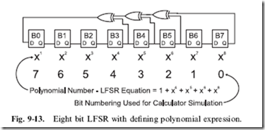
If you were going to express this LFSR to somebody else, you could send a graphic something like Fig. 9-13, or you could express it in the ‘‘polynomial’’ format like:
The polynomial format is the traditional way of expressing how an LFSR works and is used by mathematicians to evaluate an LFSR operation.
There are a few important facts about LFSRs that you should be aware of:
1. The LFSR can never have the value zero in it. If it contains zero, then none of the internal bits will ever become set.
2. The ideal LFSR implementation will be able to produce 2n – 1 different values. It should be obvious that the one value that cannot be produced is zero.
3. A poorly specified LFSR may have the situation where it ends out with a value of zero.
The operation of a single shift of the 8 bit LFSR in Fig. 9-13 can be modeled using the ‘‘C’’ function:
Hardware State Machines
The hardware state machine circuit was originally designed to allow designers to create a complex application using a simple, single ROM, a few register bits and some basic logic gates instead of a complex sequential circuit design or a processor-based solution. State machines are not widely used in modern applications because the costs of the parts needed to make up the circuit can very easily exceed that of a microcontroller. Almost ironically, hardware state machines are used as the control mechanism for most modern computer systems because they are fairly easy to design, program and debug. The use of hardware state machines (which are typically referred to as just ‘‘state machines’’) as the control mechanism for computer processors has given a new importance to the understanding of state machines.
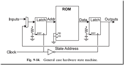
The typical ‘‘state machine’’ is shown in Fig. 9-14. This circuit consists of an ROM (usually EPROM) which has part of its output data fed back as a ‘‘state address’’. Other address lines are used as circuit inputs and the state machine changes its state address based on these inputs.
The clock is used to pass the new address to the ROM and then pass the output from the ROM to the output and input state circuits. The two latches are operated 1808 out of phase to prevent ‘‘glitches’’ from the ROM changing state from invalidly affecting any output circuits. A single edge triggered register is not typically used with the state machine because toggling inputs while the ROM is being accessed could result in invalid data being passed into the latches.
As few output bits are used as the ‘‘state address’’ as possible. The reason for this is to maximize the number of outputs and minimize the number of states which have to be programmed. Each state requires two to the number of inputs to function. Each state responds differently according to the inputs it receives.
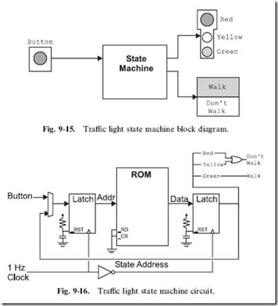
A typical application for state machines is a traffic light. If a press-button crossing light, as shown in Fig. 9-15, is considered, a state machine circuit, like that shown in Fig. 9-16 could be used.
In normal operation (which is known as ‘‘state 0’’), the green light is on and the button is not pressed. If the button is pressed, then execution jumps to state 1, which turns on the yellow light for 5 seconds (states 2, 3, 4 and 5), after which the red light is put on for 26 seconds (states 6–31). If the button is pressed during states 7–31, then execution jumps to state 6 to reset the timer.
Table 9-1 ROM programming for simple traffic light state machine.
|
State |
Button |
New state |
Green |
Yellow |
Red |
Comments |
|
B’00000’ |
1 |
B’00000’ |
1 |
0 |
0 |
Power up |
|
B’00000’ |
0 |
B’00001’ |
0 |
1 |
0 |
Power up/button press |
|
B’00001’ |
x |
B’00010’ |
0 |
1 |
0 |
Yellow LED on |
|
B’00010’ |
x |
B’00011’ |
0 |
1 |
0 |
Yellow LED on |
|
B’00011’ |
x |
B’00100’ |
0 |
1 |
0 |
Yellow LED on |
|
B’00100’ |
x |
B’00101’ |
0 |
1 |
0 |
Yellow LED on |
|
B’00101’ |
x |
B’00110’ |
0 |
1 |
0 |
Yellow LED on |
|
B’00110’ |
x |
B’00111’ |
0 |
1 |
0 |
Yellow LED on |
|
B’00111’ |
x |
B’01000’ |
0 |
0 |
1 |
Red LED on |
|
B’01000’ |
1 |
B’01001’ |
0 |
0 |
1 |
Red LED on |
|
B’01000’ |
0 |
B’00111’ |
0 |
0 |
1 |
Red LED on/reset Ctr |
|
B’01001’ |
1 |
B’01010’ |
0 |
0 |
1 |
Red LED on |
|
B’01001’ |
0 |
B’00111’ |
0 |
0 |
1 |
Red LED on/reset Ctr |
|
. . |
. . |
. . |
||||
|
B’11111’ |
1 |
B’00000’ |
0 |
0 |
1 |
Return to green |
|
B’11111’ |
0 |
B’00111’ |
0 |
0 |
1 |
Red LED on/reset Ctr |
To keep the circuit simple, I want to use an eight bit data bus ROM with six inputs (five state, one button). This means that 2**6 (or 64) states are required in the ROM. These states are listed in Table 9-1. The reset on the input address latch is used to reset the state to 0 on the power up. The button is assumed to be ‘‘pressed’’ if a ‘‘0’’ is returned.
Table 9-1 would then be converted into bits and burned into the ROM. An ‘‘x’’ means both input states have the same result on outputs.
This application is reasonable to code and build, but a problem arises with very complex state machines (ones that require tens of inputs and hundreds of different states). These state machines are normally hard coded into a custom chip rather than built out of discrete parts like I have shown for this application. The reason for placing it within a chip is to give more outputs as well as more states in a custom application. The depth and the width of the data in ‘‘real’’ applications is better suited to custom chips which can have non-custom memories added much more easily than in the situation where only commercial chips are used.
In the example above, I have used a state machine with a one second clock. Obviously in this situation there can be problems (such as the missed input if the button is pressed for less than 1 second and it isn’t released after it is pressed). This function makes state machines unattractive for rapidly changing inputs and any kind of sophisticated real-time processing of inputs is simply not economical to do with the state machine. When I say ‘‘not economical’’, I am thinking in terms of the memory and properly programming the many states.
Quiz
1. In the sequential circuit block diagram where is the clock signal passed to?
(a) To the ‘‘state memory’’ and ‘‘output formatter’’ blocks
(b) To just the ‘‘state memory’’ block
(c) To the ‘‘input formatter’’ block
(d) To the ‘‘reset control circuitry’’ block
2. Asynchronous digital logic design is being pursued because:
(a) It will result in simpler chip designs
(b) Circuitry designed under this philosophy will be easier to interface to
(c) The end of performance gains using traditional design methodologies is in sight
(d) It offers faster operations with less power usage
3. Why are edge triggered registers used for counters instead of latches?
(a) It will result in simpler circuit designs
(b) Circuitry designed under this philosophy will be easier to inter- face to
(c) Less power is required
(d) It offers faster operations with less power usage
4. Ripple counters are:
(a) Always the fastest way to implement counters
(b) Usually more complex electronically than other counter designs
(c) Always the slowest way to implement counters
(d) Similar to ripple adders in operation
5. What are advantages of serial data transmission over parallel data transmission?
(a) Reduced number of drivers and receivers
(b) Faster data transmission
(c) Lower product costs
(d) Higher product quality
6. Where is serial data transmission not used?
(a) The internet
(b) Broadcasting stations to TVs/radios
(c) Keyboard to PC interface
(d) PCI bus interfaces
7. Linear feedback shift registers are built from:
(a) The system architectural drawings
(b) The high-speed circuits to support communications
(c) Shift registers and XOR gates
(d) The basic system serial interface
8. When the value of a linear feedback shift register equals zero:
(a) The operation has completed
(b) Either the initial and input values are zero or there is a problem with the LFSR design
(c) There was an error in encrypting a message
(d) Power has been removed from the circuit
9. Hardware state machines are rarely used except in:
(a) Computer processors
(b) Military and space applications
(c) High-performance custom logic applications
(d) Situations where old ROMs are easily available
10. State machines are normally built:
(a) Out of discrete chips and ROM chips
(b) In complex custom chips
(c) On specially designed carrier PCBs
(d) With the checksum of the ROM printed on them


