Pulse Width Modulation
Despite showing how logic gates and other digital devices are built from simple analog components, they do not handle working with analog voltages very well. There are some circuits that will produce a valid analog (an arbitrary voltage, not just logic ‘‘high’’ and ‘‘low’’) voltage but they do not work very well if the circuit has to drive a high current device. Instead of varying the voltage level to provide varying levels of power, I produce a
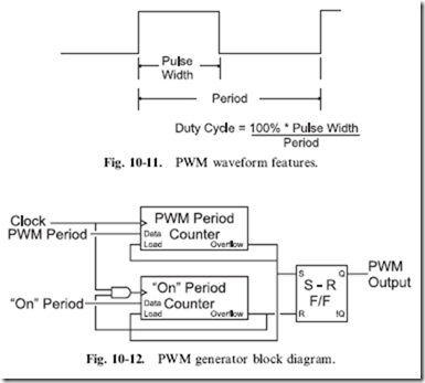
string of timed pulses known as a ‘‘pulse width modulated’’ (‘‘PWM’’) signal (Fig. 10-11). A PWM signal is a repeating signal that is ‘‘on’’ for a set period of time that is proportional to the voltage being output. I call the ‘‘on time’’ the ‘‘pulse width’’ in Fig. 10-11 and the ‘‘duty cycle’’ is the percentage of time the ‘‘on time’’ is relative to the PWM signal’s ‘‘period’’.
To output a PWM signal, there are several possible methods. One way is to use two counters that have a common clock. When one counter overflows, it resets itself and the second counter. Until the second counter overflows, the output of the circuit is set to ‘‘1’’. When the second counter overflows, the output of the circuit is reset until the first counter overflows and the process is repeated. Figure 10-12 shows how this type of circuit could be implemented.
This PWM generator circuit uses counters that are reloaded (from the ‘‘Data’’ pins) upon an ‘‘Overflow’’ positive pulse. The ‘‘PWM Period Counter’’ (the ‘‘first counter’’) runs continuously and when it overflows (reaches the final count), it resets and reloads the count value for not only itself but also for the second counter (the ‘ ‘‘ On’’ Period Counter’).
When the PWM Period Counter resets, it ‘‘Sets’’ the S-R flip flop, driving the ‘‘PWM Output’’ high for the start of the PWM signal output. The ‘‘On’’ Period Counter is reset and reloaded by the PWM Period Counter and runs until it overflows. When the ‘‘On’’ Period Counter Overflows, the PWM
Output is halted and it also stops running until the PWM Period Counter reloads it, which resets the ‘‘Overflow’’ output and allows the Counter to drive the ‘‘On’’ Period Counter once more.
Another type of PWM generator is shown in Fig. 10-13. The counter output will be continuously compared against a bit value and when the bit value is greater than the counter value, a ‘‘1’’ will be output. The block diagram for the circuit that I envisioned is shown in Fig. 10-13 and can be built quite easily as I show in this section.
When you study Fig. 10-13, there will probably be one point that won’t make sense to you: I show that the counter ranges from 0 to 14 and not 0 to 15, as you would expect for the typical four-bit counter. I wanted the counter to reset itself at 14 rather than 15 so that when the binary values were compared, a 100% duty cycle could be produced as well as a 0% duty cycle by outputting a ‘‘1’’ when the set value was greater than the counter value. If the counter ran from 0 to 15 then the circuit would not be able to produce a PWM with a 100% duty cycle.
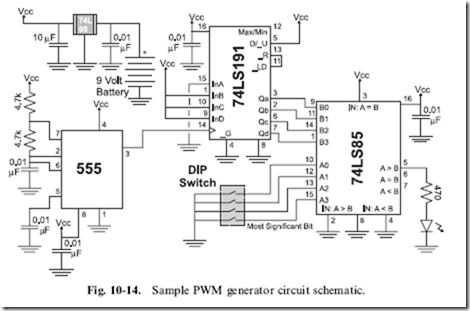
To produce the bit range from 0 to 14, I used the 74 x 191 chip counting down and tying the ‘‘_LOAD’’ pin to the ‘‘_RIPPLE’’ pin and driving the inputs to 14. The ‘‘_R’’ (‘‘Ripple’’ Output) pin becomes active when the chip is ‘‘rolling over’’ from one extreme to another and the ‘‘_LD’’ pin moves the value at the input pins into the counter’s latches when it is active. Normally, when a four-bit counter is ‘‘rolling over’’ as it counts down it goes from 0 to 15, but by tying the ‘‘_R’’ pin to the ‘‘_LD’’ (negative active ‘‘Load’’) pin of the 74 x 191, you can load in a new value when the counter reaches 0 and is about to roll over. This feature is ideal for this application as it ensures the count stays in the range of 0 to 14.
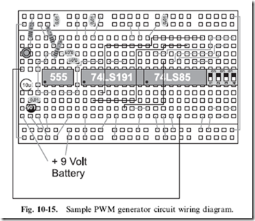
Converting the block diagram to a schematic one is very straightforward (Fig. 10-14) and wiring it onto the PCB’s breadboard is tight but not really a challenge (Fig. 10-15). The PWM output value is specified by the four- position DIP switch. I placed 0.01 mF decoupling capacitors on all of the power inputs of each of the chips. These decoupling capacitors are very important when working with the standard (not CMOS) 555 because it can place large transients on the power line.
I used TTL chips (powered by 5 volts from the 78L05 regulator) rather than CMOS chips because I found that it is difficult locating 74C85 chips.
An advantage of using TTL instead of CMOS for this circuit was that I could simply pull the comparator inputs to ground without the need of a pull up resistor. If you build this circuit with CMOS chips, make sure that you have 10 k pull up resistors on the DIP switch to ensure a high voltage is passed to the comparator.
Once you have built the circuit, you will find that the LED’s brightness will be dependent on the value on the DIP switch. It will be confusing, as the value on the DIP switch will seem to be the opposite to the behavior of the PWM. When all the switches are ‘‘on’’, the LED will be off and, for what seems to be a ‘‘large’’ value, the LED will be dim. When all the switches are ‘‘off’’ the LED will be full on. This confusion is a result of the ‘‘on’’ marking indicating when the switches are closed, not when the signal is a ‘‘1’’ or ‘‘high’’ (which is often extrapolated to being ‘‘on’’) – when the switches
are closed (‘‘on’’), the comparator input is pulled to ground and has the value ‘‘0’’.
For all PWM circuits (not just the two I’ve shown here), you must remember that the effective frequency is the input clock frequency divided by the counter value. For the example circuit shown here, the 10 kHz signal is divided by 15 (how many cycles the 74LS191 counts before resetting) so the resulting output signal frequency is 667 Hz, which is still faster than the human eye can perceive a flashing LED, but much lower than required for some DC motors. PWMs are commonly used to control the speed of electric motors and if the PWM frequency is within the audible range of human hearing, you will hear a definite ‘‘whine’’ from the motors. The solution to this problem is to either run the PWM at frequencies above human hearing (greater than 18 kHz) or below the range of human hearing (60 Hz or below).
The lower PWM frequencies should not be an issue to produce, but the higher ones can be a challenge, especially if more bits are used in the counter.
For example, to create a 20 kHz PWM output signal, you will have to provide a 300 kHz clock for a 15-value PWM and 5.1 MHz for a 255-value PWM! You may find that to get a practical circuit, you will have to find a compromise between the number of bits used in the PWM for the signal level and the speed of the oscillator that is going to be used with it.
An interesting feature of a PWM is how it can save you power. If you were to run the PWM with a 75% duty cycle, what do you think the average power output would be? If you answered 75%, then you didn’t go back in the book to look up the power formula. Power is defined by the formula:
P = V x i
and substituting in values from Ohm’s law, it can be also expressed as:
From these formulas, it should be obvious that if the voltage is high only three-quarters of the time, the power dissipated by the device being driven by the PWM is nine-sixteenths or 56% of the total power used by PWMs running with a 100% duty cycle. This means that, along with providing the ability to ‘‘throttle’’ direct current devices, a PWM can also result in significant power savings as well.
Finally, you might be confused that I gave you two quite different implementations of the PWM circuit; I did this to show you that there is almost always more than one solution to any problem. I normally recommend that new designers come up with three solutions to a problem before going ahead and implementing something. Having three solutions to choose from will allow you to compare features and drawbacks and choose the solution that is best for the application.
Button ‘‘Debouncing’’
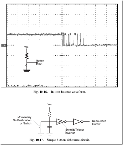
I consider the issue of debouncing switches and buttons to be one of the most important and vexing problems that you will have to deal with when you are developing applications that work with operator input. Most people think that electrical connections happen instantaneously; you might be surprised to discover that the contacts within a switch actually bounce a few times before the switch makes a constant contact. This is shown in the oscilloscope picture in Fig. 10-16.
Earlier in the book, I showed you a simple method of debouncing a switch input by creating a small memory device from two inverters. A major drawback of this circuit is that it ‘‘backdrives’’ the outputs of one of the inverters, but this problem can be eliminated through the use of CMOS inverters and a 10 k current limiting resistor. Even with this fix in place, there is another problem to consider when deciding whether or not to use this circuit – finding double throw push buttons can be difficult. This circuit is well suited for double throw switches but, from the practical difficulty of finding double throw buttons, it becomes impractical.
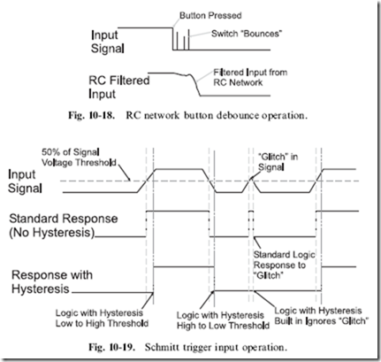
The debounce circuit that I recommend you use is shown in Fig. 10-17. This circuit consists of a resistor–capacitor network that charges over a given amount of time or discharges quickly through a closed switch or button. Figure 10-18 shows the filtering of the bouncing; it is not perfect, but it is much better than what we started with.
The inverter with the funny symbol in Fig. 10-17 is called a ‘‘Schmitt Trigger Input Inverter’’ and provides an extra measure of filtering of the button input. Schmitt trigger inputs are designed to change state on the rising or falling edge of a signal with ‘‘hysteresis’’, as shown in Fig. 10-19.
‘‘Hysteresis’’ is the property of the Schmitt trigger inputs in which the threshold point for the rising edge of the signal is different than the falling edge. Looking at Fig. 10-19, you can see that the rising edge threshold is above the ‘‘normal gate voltage threshold’’, while the falling edge threshold is less.
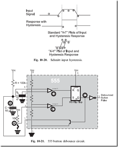
These changing threshold values are the reason for the strange symbol on the inverters, indicating Schmitt trigger inputs. Figure 10.20 shows the input versus the gate response on an ‘‘X-Y’’ chart. The ‘‘X’’ axis is the input voltage with rising voltages to the right and the ‘‘Y’’ axis represents the response of the Schmitt trigger input. By following the numbers, you can see the response of the input and that it forms the same symbol that I put on the inverter gates. For comparison, a traditional logic gate does not use this symbol – the response threshold is the same for rising and falling edge signals.
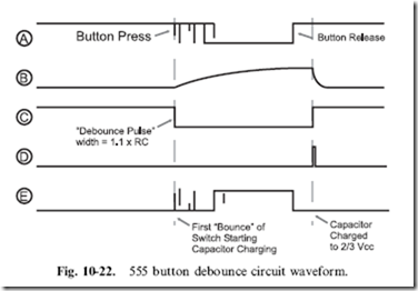
Another method of debouncing button inputs is to use a 555 or monostable circuit. In Fig. 10-21, I show a 555 wired as a monostable, driving out a pulse from a button press. The internal waveforms of the circuit
are shown in Fig. 10-22, which shows that any subsequent bouncing of the button after it makes its first connection are ignored by the circuit as the pulse is being output. If you work out the pulse time from R and C, you’ll discover that the pulse time is roughly 1 second in length. This should be long enough for a single button press to be registered and the user to remove his fingers. Obviously, this delay is too long to implement multiple buttons or even any kind of data entry functions in the circuit. To do this, you should consider the next section.
Switch Matrix Keypad Interfacing
As I ended off the previous section, you cannot use simple button debouncing techniques to implement a large number of buttons or even a keyboard for data entry. Just so there’s no confusion, I consider a ‘‘large number of buttons’’ to be four or more; providing individual debounce circuits for anything more than a couple of buttons is expensive and time consuming. Along with the cost and time involved, you will also have to come up with some way of prioritizing the button inputs and recognizing non-standard keys like ‘‘shift’’ and ‘‘control’’.
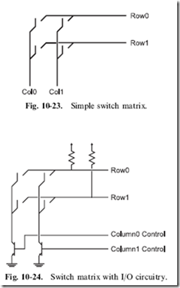
The keys and buttons in PC keyboards and numeric keypads are arranged in ‘‘rows’’ and ‘‘columns’’ and they can be drawn out in such a way that they look like a ‘‘matrix’’. A ‘‘momentary on’’ switch is placed at the intersection of each row and column, as shown in Fig. 10-23. This ‘‘switch matrix’’ provides the ability to ‘‘scan’’ a large number of button inputs with a relatively small number of lines. Your PC’s 104/105 keyboard usually has a 22 by 7 matrix connection to a microcontroller, which scans through the keys and reports any key presses using the algorithms presented in this section.
Keyboards with a 100 keys or more are an extension of the four-button key matrix shown in Fig. 10-23 and have the same concerns and issues to watch out for.
You probably cannot see immediately how the individual keys or buttons of the switch matrix shown in Fig. 10-23 can be polled, but the operation will probably become clearer when you see the resistors and transistors I’ve added to the switch matrix in Fig. 10-24.
In this case, by connecting one of the columns to ground, if a switch is closed, the pull down on the row will connect the line to ground. When the row is polled by an I/O pin, a ‘‘0’’ or low voltage will be returned instead of a ‘‘1’’ (which is what will be returned if the switch in the row that is connected to the ground is open due to the pull up on it). To scan the keyboard, the column transistors are turned on, one at a time, and while the column transistor is on and the column is pulled to ground, the rows are compared to a logic level of ‘‘0’’, which would indicate that the button is pressed.
This methodology for handling switch matrix keypad scans I’ve outlined here probably seems pretty simple. Depending on your familiarity with programming and different microprocessors and microcontrollers, you will probably realize that implementing these functions could be done even simply in assembly language programming or ‘‘C’’. You should also realize that this code would be quite difficult to implement just using logic chips.
To avoid the complexities of trying to develop TTL logic that will carry out the functions described in the pseudo-code presented above, I normally
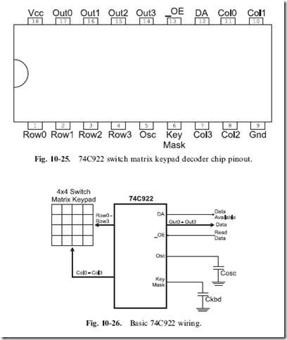
use the 74C922 keypad decoder chip (Fig. 10-25). This chip can be used to debounce and encode up to 32 buttons (although 16 is the normal maximum) and carries out button debouncing internally as well as keeping track of two currently held-down keys when new keys are pressed. The 74C922 is quite easy to wire to a four by four (16 button) switch matrix keypad, as shown in Fig. 10-26. By ‘‘doubling up’’ rows of sensors of the 74C922, you can add a number of additional keys to the application. In the next section, I will show how this is done to create a 20 button input device (with up to 32 possible).
The two capacitors are used to create a relaxation oscillator within the chip that is used to ‘‘scan’’ through the buttons as well as provide a ‘‘debounce’’ delay count for the application. The two capacitor values are calculated as:
I like a debounce interval of 20 ms: plugging this into the formulas above, I get a value of 2 mF and 20 mF. When I build my own applications, I tend to have a lot of 10 mF (for power filtering) and 1 mF (for MAX232 RS-232 level converters) electrolytic capacitors on hand. I have not found any problems with using these components and I would recommend that you use them as well to avoid having to stock multiple capacitor values for different applications.
Quiz
1. What are ideal sequential circuit interfaces?
(a) LCDs
(b) Individual switches and LEDs
(c) Keyboards
(d) USB flash disks
2. What is the suggested digital electronics interface to an Hitachi 44780 controlled LCD display?
(a) Hardware state machine
(b) Microcontroller
(c) Sequential circuit
(d) Combinatorial circuit
3. Is a bus ‘‘Read’’ or ‘‘Write’’ faster?
(a) Write is faster
(b) Read is faster
(c) Using a synchronous clocked circuit, they take the same amount of time
(d) Read is slower due to the need to retrieve data from the inter- face device
4. Seven-segment LED displays have a common:
(a) LED anode or cathode
(b) Segment pins
(c) LED drivers built into the package
(d) Pin interface that is used by all devices, regardless of the number of digits in the package
5. Multiple seven-segment LED displays show different values by using:
(a) Linear feedback shift registers that have encoded the bit patterns
(b) Turning on each individual digit with its unique value periodically
(c) Multiple LED driver circuits that drive the value for its respective digit to the LED display
(d) Multiple bits of memory, one for each segment, which are loaded according to the display value
6. For a PWM circuit running its logic at 5 volts and a duty cycle of 67%, what is the ‘‘on’’ voltage level of the output signal?
(a) 0.67 volts
(b) 5 volts
(c) 2/3 volts
(d) 3.35 volts
7. The power dissipated by a PWM running with a 20% duty cycle will be what fraction of a 100% duty cycle?
|
(a) |
0.04 |
|
(b) |
40% |
|
(c) |
0.4 |
|
(d) |
400% |
8. A 555 monostable with R ¼ 100 k and C of 4.7 mF will output a pulse of:
(a) Approximately 0.5 s
(b) Approximately 4.7 s
(c) Approximately 1.1 s
(d) Insufficient data given to determine the pulse width
9. Rows and columns in a switch matrix keypad have what connected to them?
(a) The rows have a transistor connected to ground and the columns have a capacitor
(b) The columns have transistors connected to ground and the rows are left open
(c) The columns are left open and the rows have a transistor connected to ground
(d) The columns have transistors connected to ground and the rows have pull up resistors
10. The 74C922 reads a switch matrix keypad by:
(a) Pulling the columns of a switch matrix keypad to ground and scanning the rows for pulled down bits
(b) Driving a 1 kHz square wave on the rows and polling the
columns for the signal
(c) Using an internal microprocessor
(d) Measuring the capacitances of individual lines and looking for changes

