Complex Sequential
Circuits
As the saying goes: ‘‘You now know enough to be dangerous.’’ You should be fairly comfortable with working with logic functions and equations, have an understanding of electronics and how to interface logic chips (of different families together), understand the basics of memory and have gone through a number of clocking schemes. I’m sure that you now feel you are ready to start bringing these pieces together into some interesting applications. I’m sure that you have some ideas of things you would like to have your hand at designing. Before being set free to wreak havoc on an unsuspecting world, I want to spend some time presenting you with some chips and tools that will make your plans for world domination much easier. In this chapter, I want to go through some of the subsystems that are available in chips that will make your design work easier.
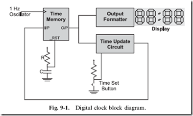
In Chapter 7, I introduced you to the digital clock block diagram shown in Fig. 9-1. There shouldn’t be any part of this diagram that is a surprise to you; the ‘‘time memory’’ consists of a number of flip flop registers that are reset
upon power up. The ‘‘time update circuit’’ consists of an adder along with logic and a user push button to determine what the next time will be. The ‘‘output formatter’’ consists of logic to decode the time memory and display it on a set of LEDs. Finally, the 1 Hz clock can be produced a number of different ways that are covered in the previous chapter.
While I must admit that it would be cool to see a digital clock designed using two input logic gates, I want to point out that there are a number of commonly available chips that provide major subsystems needed for such an endeavor. For the rest of this book I will be focusing on these chips and how they are interconnected to form ‘‘real world’’ applications.
Virtually all of these chips are sequential circuits in their own right; consider a ‘‘counter’’ chip that increments its internal memory devices each time a rising clock edge is received. The counter chip consists of several flip flop bits and combinatorial logic that processes input data, provides the value increment and outputs the data in a specific format. These functions are very similar to that provided by the digital clock in Fig. 9-1.
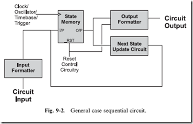
To show what I mean, consider the sequential circuit block diagram in Fig. 9-2. Superficially, the diagram has a very strong resemblance to Fig. 9-1 because many of the same basic functions and capabilities are required in both instances.
The ‘‘state memory’’ is the current operating state of the chip. The term ‘‘state’’ simply means at what operating point the chip is at. For a counter or other arithmetic function chip, the term ‘‘state’’ probably seems somewhat grandiose, but it is an accurate way of describing the current value in a counter. For a microprocessor, the term ‘‘state memory’’ is almost an understatement, as it includes not only the program counter (which points to the next instruction to execute) but also data and status register information.
The state memory can be reset (as shown in the previous chapter) and, more importantly, it is usually the only point in which the clock/oscillator input is received. The philosophy behind most sequential circuits is that the combinatorial logic processing input, output and the next state information, regardless of the circumstances, will be available in time for the next active clock cycle. The term normally used to describe this methodology of design is ‘‘synchronous’’ because a central clock is keeping track of the operations within the chip.
This philosophy is currently under challenge from scientists interested in investigating ‘‘asynchronous’’ digital logic design. This effort involves designing sequential circuits that are not ‘‘paced’’ by a central clock, but the length of time of each operation. For example, moving data from one register to another should take much less time than an instruction which stores data in the main memory. Asynchronous digital logic design holds the promise of faster computers that use much less power because the only active circuitry are the required gates and flip flops of the current time – nothing else needs to be active, nor do other circuits need to be clocked.
The ‘‘next state update circuit’’ and ‘‘input formatter’’ blocks process the current bit data and any relevant input for storage in the state memory. In Fig. 9-1, I combined both of these functions into the ‘‘time update circuit’’ because the only input required for this clock is whether or not the ‘‘time set button’’ is pressed – if it is, then the time update circuit will increment the hours, minutes and seconds stored in the digital clock’s ‘‘time memory’’.
The ‘‘input formatter’’ circuitry can be processing different inputs controlling what the next state is going to be – this is why I link it to the ‘‘next state update circuit’’. For a counter, this information could be the direction the counter executes in or whether or not the counter counts in binary or BCD.
The output formatter converts data into the required output and provides appropriate drivers for the function. Note that I have drawn a link to this box from the ‘‘reset control circuitry’’ despite my statement earlier that only the state memory could be reset. The reason for drawing in this link is to indicate that the chip may have tri-state drivers and these are held in a high impedance (‘‘off ’’) condition while reset is active.
As you work through the material in the rest of the book, try to see how the described chip functions fit in with this model. You might have a better model to work with that makes more sense to you and if this is the case use it. The model that’s presented here allows me to visualize what is happening in an application, and it would be arrogant of me to assume that it works for everyone else.
Counters
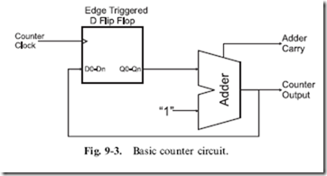
One of the most useful functions that you will use when you develop digital electronic circuits is the counter. The counter is actually a smaller piece of many complex chips, as it provides a basic way of maintaining the current operating state along with a method of progressing to the next one. The basic counter circuit consists of a set of flip flops that drive into and are driven from an adder. A counter circuit is shown in Fig. 9-3. The use of ‘‘edge triggered’’ flip flops is a very important aspect of the circuit shown in Fig. 9-3 and one that you should keep in mind. When the ‘‘counter clock’’ changes state, the output value of the adder (which is the D flip flop value plus 1) is presented to the inputs of the D flip flop register bits as the next value to be saved.
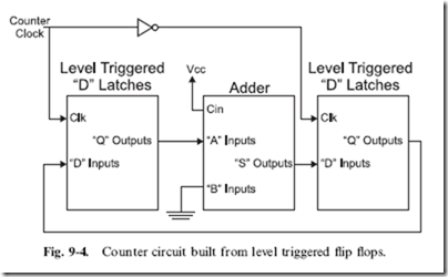
If an edge triggered flip flop register wasn’t used in the circuit, then you would have to use latches and design the counter something like the one shown in Fig. 9-4. In this circuit, I have put in two latches, each one ‘‘out of phase’’ with each other. This is to say that when the clock is high, one latch is storing the data while the other is passing through the value presented at its inputs. When the clock changes value, the latches change from passing data to storing and vice versa. This method of implementing a counter is unnecessarily complex and potentially very slow – the extra set of flip flops will slow down the performance of the counter and limit its maximum speed.
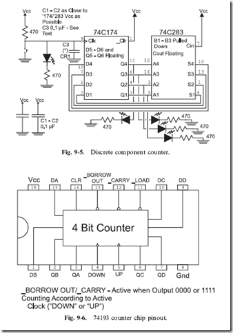
The counter circuit of Fig. 9-3 can be built using a 74C174 hex D flip flop and a 74C283 four bit adder circuit. The circuit shown in Fig. 9-5 will demonstrate how the counter works. When the term ‘‘floating’’ is used with respect to pins, it means that the pins are left unconnected.
When you try out this circuit, the first thing that you will probably notice is that when you press the button, the LEDs will not ‘‘increment’’ by 1, but by 2, 3 or even 4. The reason for this is known as ‘‘switch bounce’’. Earlier in the book, I showed a two inverter circuit for eliminating switch bounce, and later I will discuss a number of other strategies for minimizing the problem. For now, if you wire a 0.1 f,LF tantalum capacitor as shown in Fig. 9-5, you should minimize this problem (although you will probably not eliminate it).
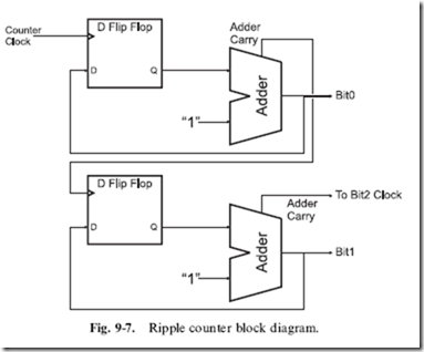
The counter circuit should work well for you. As with the previous projects, a single chip can be used where multiple required. The counter chip that I usually work with is the 74LS193 (Fig. 9-6) which combines a four bit D flip flop register and adder along with the ability to decrement the result. Later in the book, I will show how this chip can be used with others to ‘‘cascade’’ from a 4 bit counter to an 8 and 16 bit counter.
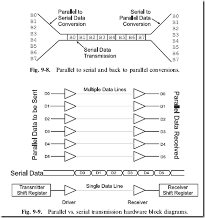
The ‘‘_Carry’’ out bit of the 74193 can be passed from one counter to the clock input of another to provide the ability to count more bits, as I show in Fig. 9-7. The carry bit can be thought of as an overflow to the more significant counter, indicating that it should increment its value. If by looking at this circuit you recognize it as being similar to the ‘‘ripple’’ adder presented earlier
in the book, go to the head of the class. This circuit is known as a ‘‘ripple counter’’ and does not have the same high speed as a counter built from look- ahead carry adders.
Along with the 74193, you might want to consider the 74161 counter,
which can only count up and changes to the count value must be clocked in (the 74193 allows changes to the count value asynchronously, which is to say without the clock). The 74160 and 74192 chips are identical to the 74161 and 74193, respectively, but only count up to 9 and are known as ‘‘decade’’ counters. The 74160 and 74192 are useful in circuits in which the digits 0 through 9 are required for counting.
Shift Registers
Most intersystem (or intercomputer) communications are done serially. This means that a byte of data is sent over a single wire, one bit at a time, with the timing coordinated between the sender and the receiver. So far in this book, if you were to transfer a number of bits at the same time, you would send them in ‘‘parallel’’, one connection for each bit. The basis for serial communications is the ‘‘shift register’’, which converts a number of ‘‘parallel’’ bits into a time-dependent single string of bits and converts these strings of bits back
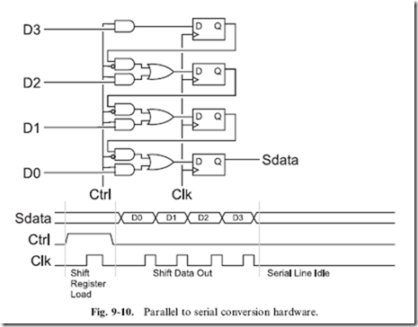
into a set of parallel bits. Figure 9-8 shows this process with eight parallel data bits being converted into a bit stream and transmitted to a receiver, which ‘‘recreates’’ the eight bits back into their parallel data format.
The differences between serial and parallel data transfers are shown in Fig. 9-9. To send six bits in parallel, a half dozen transmitting ‘‘drivers’’ and an equal number of ‘‘receivers’’ are required. To send six bits serially, just a single driver and receiver is required, but the sending circuit must have a ‘‘shift register transmitter’’ and the receiving circuit must have a ‘‘shift register receiver’’. The parallel data can be sent in the time required for just one bit while the serial data requires enough time to send each of the six bits individually.
It probably looks like transmitting data serially requires a lot of overhead and it slows down the data transfer. There are a number of factors to consider before making this assumption. The first is that most chips are not made out of individual logic gates as the simple chips presented here so far; they are
usually very dense circuits consisting of thousands of gates, with the impact of adding serial shift registers being very minimal. Another issue to consider is that it can be very difficult to synchronize all the parallel bits to ‘‘arrive’’ at the receiver at the same time in high-speed circuits. Finally, multiple wires can take up a lot of space and be quite expensive; if chips or subsystems could have shift registers built into them, then it often makes sense (both practical and economic) that data be transferred serially.
The circuit that converts the parallel data into the serial stream is quite simple. Figure 9-10 shows a circuit along with a waveform showing how the circuit works. Four bits are first loaded in parallel into a series of four flip flops. These four flip flops can be driven with data either from an external source or from the next significant bit depending on the ‘‘Ctrl’’ bit state. If ‘‘Ctrl’’ is high, when the ‘‘Clk’’ (‘‘clock’’) is cycled, the data in the D3:0 bits are stored in the four flip flops. If ‘‘Ctrl’’ is low, when ‘‘Clk’’ is cycled, each bit is updated with its next significant bit and data is shifted out, least significant bit first.
The process of each bit of data ‘‘passing’’ through each of the flip flops is known as ‘‘shifting’’. As can be seen in Fig. 9-10 that four data bits are ‘‘shifted’’ out on the ‘‘Sdata’’ line in ascending order, with the ‘‘Clk’’ line specifying when a new bit is to be shifted out. If this method was used to
transmit data between two digital devices, it would be known as ‘‘synchronous serial data transmission’’.
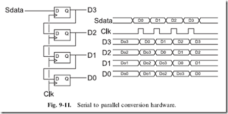
Receiving ‘‘Sdata’’ is accomplished by simply using four flip flops wired with their outputs wired to the next input, as I’ve shown in Fig. 9-11. The same clock that is used to shift out the data from the transmitter should be used to shift in the data in the receiver. Along with the circuit used to shift in the data, I have included a waveform diagram for you to take a look at in Fig. 9-11. One potentially confusing aspect of the waveforms is my use of the ‘‘DoX’’ convention to indicate the previous values within the receiver. These bits will be shifted out in a similar manner as to how the data was shifted in.
There are a number of very common synchronous data protocols that are used in computer systems to provide simple interfaces to common peripherals. These interfaces, which include ‘‘Microwire’’, ‘‘SPI’’ and ‘‘I2C’’, are very easy and relatively fast ways of adding peripherals such as analog to digital converters and external memory to microcontrollers and complete computer systems. In fact, your PC has an I2C processor peripheral bus for controlling power supplies and monitoring the processor’s chip temperature.
