Reading Datasheets
I’ve never understood why college and university courses do not give an introductory course in reading digital electronic device datasheets. Despite how prepared you are for them, you will feel quite overwhelmed the first time you have to look through a number of datasheets trying to find a part that meets your requirements. When I first started working with electronics, datasheets were generally quite poor, with only a few standout companies providing good documentation for their chips. Fortunately, this has changed over the past 10 years, the Internet and the capability of downloading good- quality datasheets being almost a marketing tool to help engineers select the parts they are going to use in their designs.
Personally, I find it more daunting to look at datasheets over the Internet because they are generally encoded as Adobe Acrobat pdfs that take a while to load and you can never flip the pages on the screen as fast as you would like. To make matters worse, it can be very difficult to put multiple datasheets up on a computer display to allow you to compare the features of the different chips. This difficulty gives rise to the most important recommendation that I can make about downloading datasheets from the Internet – print them out! I have several binders of printed out datasheets for parts that I often use. By printing them out, I have immediate access to them and I can flip back and forth between pages effortlessly. It is my opinion that documentation shouldn’t be ‘‘paperless’’.
The first sheet of the datasheet is usually a one page description of the part. It normally contains:
1. Part number
2. High-level part description
3. Part pinout
4. Common/related/pin compatible parts
5. Important chip features
6. Basic operations truth table
When looking at a datasheet, you should first check out the part number of the datasheet versus what you are interested in. This means that you should be checking not only the numeric code for the device but also the high-level identifier and the technology identifier. For example, if you were looking for a low-power TTL dual input NAND gate and looked up the datasheet based on a web search for ‘‘TTL dual input NAND’’, you could see such diverse part numbers as:
74LS00
74C00
54LS00
74W00
74ALS03
with the question being: Which is the one that you want?
For these parts the high-level identifier is the ‘‘74’’ or ‘‘54’’. In this book, I have focused on the 74 series of logic – but if you look at ‘‘54’’ series logicyou will see that its operation is identical and may decide to go ahead and order the parts. This could be a big problem because ‘‘54’’ series parts are military-grade chips and they tend to cost 10 times that of standard ‘‘74’’ series logic and do not necessarily have the same pinout as ‘‘74’’ series chips.
The technology identifier is the letter code between the high-level identifier and the part number. In the list of five chips above, I have presented traditional TTL low-power logic (‘‘LS’’), CMOS logic (‘‘C’’), advanced Shottkey low power (‘‘ALS’’) and single gate CMOS (‘‘W’’). The danger of not reading the datasheet’s part number is that you could end up ordering the wrong part number, resulting in higher than expected costs and lost time looking up and reordering the correct part.
Always read through the datasheet’s first page high-level part number description. This can range from a single sentence to four or five bulleted items. Like the part number check, this should just be a filter operation, resulting in you making sure the part will do essentially what you want it to do.
The part pinout is something that is critical to know when you are wiring a circuit. Except for the wiring experiments presented in this book, I have
listed only a few part pinouts because a part’s pinout may vary between manufacturers of the same part and they may vary according to the packaging type. The part pinout may also change according to packaging technology. It isn’t unusual to see a pin through hole (PTH) packaged chip with a specific pinout but its surface mount technology (SMT) sibling having extra pins or different connections to different pin numbers. I’m sure that both of these statements are a bit hard to understand; you might be thinking that the part numbers are standard. I wish I could tell you how many times I have been bitten by these two little traps. Circuit design systems also make assumptions about part pinouts based on the pinouts from specific manufacturers and don’t bother checking the pinouts from others.
The important chip features listed on the front page of the datasheet will not list the features of the chip to the lowest possible level, but it will give you some ideas about how the chip works and if there are any issues that could be a problem with you using the chip in your application.
A lot of times you will discover that a part will not have exactly the functions that you want but, by checking the datasheet, it may list related parts that provide a similar function that you can take a look at. Finally, for very simple chips, the front page of the datasheet will present you with truth tables describing the operation of the chip or the different parts of the chip.
The front page of a chip’s datasheet can be incredibly useful to you and by spending a few minutes familiarizing yourself with it, you can decide whether or not the chip is appropriate for your application without having to delve into the minutia of the following pages.
Chip Operating Characteristics
An important feature of the datasheet is the ‘‘operating characteristics’’ for the chip. This section of the datasheet explains such operating parameters as:
1. Input pin voltage thresholds and currents
2. Output voltages along with current source and sinking capabilities
3. Gate delay timing
4. Expected input and output pin line impedances
5. Miscellaneous operating information.
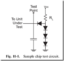
Each chip datasheet lists the logic thresholds, along with their characteristics when subjected to different parameters. Often you will see a two-axis graph, with a curve showing the chip characteristic response to the changing input parameters. This part of the drawing should not be difficult to understand but what can be confusing is the small schematic marked as a ‘‘test circuit’’ that often accompanies the graph. An example of such a schematic is shown in Fig. 11-1; it shows the circuit that was connected to the pin while the test was taking place. These test circuits simulate other circuits connected to the chip, helping to ensure that the chip is operating as it would in a typical application.
The output voltage and current characteristics are really a function of the logic technology used and not unique to the individual chip’s pins.
If you were to read other datasheets of chips built from the same technology you would discover that the output parameters are the same between the two chips and, by extrapolation, all the chips built from this technology. If you were to search the manufacturer’s web site, you would discover that this information has been published for all parts in the technology family and the information in the chip’s datasheet is really redundant. The reason why the information is repeated in the individual chip’s datasheets is to minimize the amount of cross-checking that you will have to do.
The previous comment could be made about gate delay timing but there is a wrinkle in the specification in the datasheet. Is the quoted ‘‘gate delay’’ for the chip function or for the individual basic technology gate (i.e. the ‘‘NAND’’ gate for TTL)? Normally, the datasheet will list the chip function gate delay instead of the basic technology gate delay because the actual gate delay is probably less than the product of the basic gate delay time multiplied by the number of gates the signal has to pass through.
As you learn more about electronics, you learn that not only do wire connections have resistance but they also have capacitance and impedance.
All these factors affect the transmission of data signals and are known by the term ‘‘characteristic impedance’’. Printed circuit boards (PCBs) have a characteristic impedance of 55 Q (the coax cable that sends signals to your TV has a characteristic impedance of 75 Q). The input and output pins must be designed to match with the 55 Q PCB characteristic impedance to ensure that signals pass between pins as efficiently as possible.
All these chip characteristics and any miscellaneous data that the chip manufacturer feels important enough to include should be read through and understood in order to best wire a chip into your application circuit.
IEEE Logic Symbols
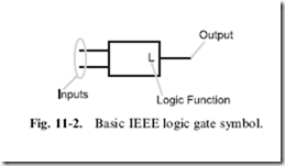
When you look at some datasheets, you will see the function of the chip described using a graphical system that is different from the one that I have used in this book. Instead of unique shapes for each gate, they are represented as a rectangular block like the one in Fig. 11-2. These blocks are part of the ‘‘IEEE Standard Graphic Symbols for Logic Functions’’. This standard is often used to describe the operation of a chip instead of the graphical symbols that I have used in the book.
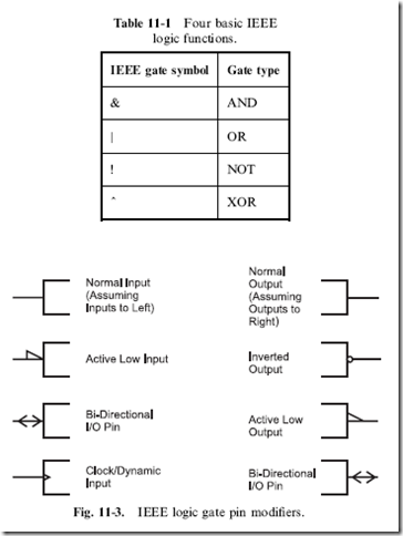
The IEEE gate definition contains a single character to indicate what the function is. Table 11-1 lists the basic characters and their functions. For
negated outputs and inputs, the gate pin modifiers presented in Fig. 11-3 are used. Note in Table 11-1, only the four unique gate functions are listed – NAND and NOR gates are represented with the gate modifiers shown in Fig. 11-3.
For the complete IEEE logic symbol definition, I suggest that you download and printout ANSI/IEEE Std 91a-1991 from:
http://www.ee.ic.ac.uk/pcheung/teaching/ee1_digital/logic symbols.pdf
This document outlines the conventions used to identify each of the different functions used to describe different logic functions in the IEEE standard format. This method of presenting chip functions may seem to be rather difficult to decode when you first see it, but after you’ve worked with it a while, it will become second nature to you.
Having said this, I would suggest that you avoid working with these symbols until you are very familiar with working with digital electronics.
The standard graphic symbols have been well thought out and are immediately recognizable when you are first learning to work with digital electronics and logic gates. The IEEE symbols can be difficult to distinguish when you are first starting out and you can very easily get yourself into trouble if you misread a symbol or forget the purpose of a pin modifier.
Power Usage and Fanouts
An important consideration for selecting a chip is the amount of power dissipated. This information is necessary not only for the individual gate but also for the complete application. The sum of all the power is the total power needed by the application and this value will dictate the power methodology used as well as the cooling requirements for the final product. While not explicitly a correlation, you will find that the more power a logic technology uses, the more external inputs that can be driven (this is the technology’s ‘‘fanout’’).
When you look at a chip’s current (which is related to its power) consumption, remember to look at not only the current required to power the
gate but also at maximum input sinking and output sourcing or sinking. These currents should all be added together to get the worst-case power consumed by the chip. I have seen a number of products where the designer expressed the power consumption by what he thought was a ‘‘typical case’’ and found out that the actual current consumption is somewhat higher and the specified power supply did not have sufficient margin for the product to work reliably.
Along with the current consumption, the datasheet should also specify
the number of input pins the chip’s output pins can drive. It is important to note that the number of input pins quoted is the same technology as the chip. When you are mixing technology, you will have to understand the
input current requirements of the input pins and, as ‘‘a rule of thumb’’, make sure that the total current drawn by the input pins does not exceed 50% of the total sinking current capability of the output pin. This will ensure that the logic functions will be at the correct levels regardless of the circumstances.
Actually, I would recommend that for your first applications, you never drive more than three inputs from a single output and strive to drive no more than two outputs in the design. Marginal signals due to overloaded output pins are very difficult to recognize from the failure symptoms and difficult to confirm when the problem is suspected.
Quiz
1. What isn’t on the first page of the datasheet?
(a) Part number
(b) Part pinout
(c) Chip cost
(d) Important chip features
2. What is the technology identifier in the part number ‘‘74S174’’?
(a) 174
(b) 74
(c) 74S
(d) S
3. What parameter isn’t a chip operating characteristic?
(a) Gate delay timing
(b) Chip logic function
(c) Input pin voltage thresholds and currents
(d) Expected input and output pin line impedances
4. The chip gate delay specification
(a) Is for ideal conditions
(b) Is for the basic technology gate delay
(c) Is for the chip function
(d) Is for the NAND gate delay
5. IEEE symbols
(a) Will replace the standard graphical symbols
(b) Represent negative output functions by placing a symbol on the output pin
(c) Is used to define all chips
(d) Are only used for basic logic gates
6. Starting out using IEEE symbols
(a) Is a bad idea as the symbols are not immediately recognizable
(b) Is the recommended way to learn about digital electronics
(c) Will help you design highly optimized digital electronics circuits
(d) Will encourage you to buy from manufacturers that properly document their products
7. When planning for the current consumption of a product, which current specification should be ignored?
(a) Standby current
(b) Output low current sink
(c) Input low current drain
(d) None
8. The maximum number of inputs a single output can drive is:
(a) Determined by the total current drawn by the inputs
(b) Three in all cases
(c) The output sink current specification divided by the average input current drain
(d) Infinite


