Boolean Algebra and Digital Logic
3.1 Introduction
“I’ve always loved that word, Boolean.”
-Claude Shannon
George Boole lived in England during the time Abraham Lincoln was getting involved in politics in the United States. Boole was a mathematician and logician who developed ways of expressing logical processes using algebraic symbols, thus creating a branch of mathematics known as symbolic logic, or Boolean algebra. It wasn’t until years later that Boolean algebra was applied to computing by John Vincent Atanasoff. He was attempting to build a machine based on the same technology used by Pascal and Babbage, and wanted to use this machine to solve linear algebraic equations. After struggling with repeated failures, Atanasoff was so frustrated he decided to take a drive. He was living in Ames, Iowa, at the time, but found himself 200 miles away in Illinois before he suddenly realized how far he had driven.
Atanasoff had not intended to drive that far, but since he was in Illinois where he could legally buy a drink in a tavern, he sat down, ordered a bourbon, and realized he had driven quite a distance to get a drink! (Atanasoff reassured the author that it was not the drink that led him to the following revelations-in fact, he left the drink untouched on the table.) Exercising his physics and mathematics backgrounds and focusing on the failures of his previous computing machine, he made four critical breakthroughs necessary in the machine’s new design.
He would use electricity instead of mechanical movements (vacuum tubes would allow him to do this).
Because he was using electricity, he would use base 2 numbers instead of base 10 (this correlated directly with switches that were either “on” or “off “), resulting in a digital, rather than an analog, machine.
He would use capacitors (condensers) for memory because they store electrical charges with a regenerative process to avoid power leakage.
Computations would be done by what Atanasoff termed “direct logical action” (which is essentially equivalent to Boolean algebra) and not by enumeration as all previous computing machines had done.
It should be noted that at the time, Atanasoff did not recognize the application of Boolean algebra to his problem and that he devised his own direct logical action by trial and error. He was unaware that in 1938, Claude Shannon proved that two-valued Boolean algebra could describe the operation of two-valued electrical switching circuits. Today, we see the significance of Boolean algebra’s application in the design of modern computing systems. It is for this reason that we include a chapter on Boolean logic and its relationship to digital computers.
This chapter contains a brief introduction to the basics of logic design. It provides minimal coverage of Boolean algebra and this algebra’s relationship to logic gates and basic digital circuits. You may already be familiar with the basic Boolean operators from a previous programming class. It is a fair question, then, to ask why you must study this material in more detail. The relationship between Boolean logic and the actual physical components of any computer system is very strong, as you will see in this chapter. As a computer scientist, you may never have to design digital circuits or other physical components-in fact, this chapter will not prepare you to design such items. Rather, it provides sufficient background for you to understand the basic motivation underlying computer design and implementation. Understanding how Boolean logic affects the design of various computer system components will allow you to use, from a programming perspective, any computer system more effectively. For the interested reader, there are many resources listed at the end of the chapter to allow further investigation into these topics.
3.2 Boolean Algebra
Boolean algebra is an algebra for the manipulation of objects that can take on only two values, typically true and false, although it can be any pair of values. Because computers are built as collections of switches that are either “on” or “off,” Boolean algebra is a very natural way to represent digital information. In reality, digital circuits use low and high voltages, but for our level of understanding, 0 and 1 will suffice. It is common to interpret the digital value 0 as false and the digital value 1 as true.
3.2.1 Boolean Expressions
In addition to binary objects, Boolean algebra also has operations that can be performed on these objects, or variables. Combining the variables and operators yields Boolean expressions. A Boolean function typically has one or more input values and yields a result, based on these input values, in the range {0,1}.
Three common Boolean operators are AND, OR, and NOT. To better understand these operators, we need a mechanism to allow us to examine their behaviors. A Boolean operator can be completely described using a table that lists the inputs, all possible values for these inputs, and the resulting values of the operation for all possible combinations of these inputs. This table is called a truth table. A truth table shows the relationship, in tabular form, between the input values and the result of a specific Boolean operator or function on the input variables. Let’s look at the Boolean operators AND, OR, and NOT to see how each is represented, using both Boolean algebra and truth tables.
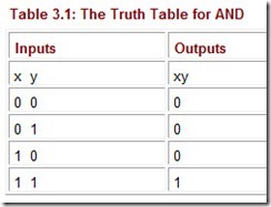
The logical operator AND is typically represented by either a dot or no symbol at all. For example, the Boolean expression xy is equivalent to the expression x * y and is read “x and y.” The expression xy is often referred to as a Boolean product. The behavior of this operator is characterized by the truth table shown in Table 3.1.
The result of the expression xy is 1 only when both inputs are 1, and 0 otherwise. Each row in the table represents a different Boolean expression, and all possible combinations of values for x and y are represented by the rows in the table.
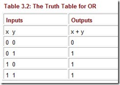
The Boolean operator OR is typically represented by a plus sign. Therefore, the expression x + y is read “x or y.” The result of x + y is 0 only when both of its input values are 0. The expression x + y is often referred to as a Boolean sum. The truth table for OR is shown in Table 3.2.
We now understand that Boolean algebra deals with binary variables and logical operations on those variables. Combining these two concepts, we can examine Boolean expressions composed of Boolean variables and multiple logic operators. For example, the Boolean function:
is represented by a Boolean expression involving the three Boolean variables x, y, and z and the logical operators OR, NOT, and AND. How do we know which operator to apply first? The rules of precedence for Boolean operators give NOT top priority, followed by AND, and then OR. For our previous function F, we would negate y first, then perform the AND of ![]() and z, and lastly OR this result with x.
and z, and lastly OR this result with x.
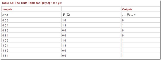
We can also use a truth table to represent this expression. It is often helpful, when creating a truth table for a more complex function such as this, to build the table representing different pieces of the function, one column at a time, until the final function can be evaluated. The truth table for our function F is shown in Table 3.4.
The last column in the truth table indicates the values of the function for all possible combinations of x, y, and z. We note that the real truth table for our function F consists of only the first three columns and the last column. The shaded columns show the intermediate steps necessary to arrive at our final answer. Creating truth tables in this manner makes it easier to evaluate the function for all possible combinations of the input values.
3.2.2 Boolean Identities
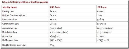
Frequently, a Boolean expression is not in its simplest form. Recall from algebra that an expression such as 2x + 6x is not in its simplest form; it can be reduced (represented by fewer or simpler terms) to 8x. Boolean expressions can also be simplified, but we need new identities, or laws, that apply to Boolean algebra instead of regular algebra. These identities, which apply to single Boolean variables as well as Boolean expressions, are listed in Table 3.5. Note that each relationship (with the exception of the last one) has both an AND (or product) form and an OR (or sum) form. This is known as the duality principle.
Table 3.5: Basic Identities of Boolean Algebra
The Identity Law states that any Boolean variable ANDed with 1 or ORed with 0 simply results in the original variable. (1 is the identity element for AND; 0 is the identity element for OR.) The Null Law states that any Boolean variable ANDed with 0 is 0, and a variable ORed with 1 is always 1. The Idempotent Law states that ANDing or ORing a variable with itself produces the original variable. The Inverse Law states that ANDing or ORing a variable with its complement produces the identity for that given operation. You should recognize the Commutative Law and Associative Law from algebra. Boolean variables can be reordered (commuted) and regrouped (associated) without affecting the final result. The Distributive Law shows how OR distributes over AND and vice versa.
The Absorption Law and DeMorgan’s Law are not so obvious, but we can prove these identities by creating a truth table for the various expressions: If the right-hand side is equal to the left-hand side, the expressions represent the same function and result in identical truth tables. Table 3.6 depicts the truth table for both the left-hand side and the right-hand side of DeMorgan’s Law for AND. It is left as an exercise to prove the validity of the remaining laws, in particular, the OR form of DeMorgan’s Law and both forms of the Absorption Law.
Table 3-6: Truth Tables for the AND Form of DeMorgan’s Law
The Double Complement Law formalizes the idea of the double negative, which evokes rebuke from high school teachers. The Double Complement Law can be useful in digital circuits as well as in your life. For example, let x be the amount of cash you have (assume a positive quantity). If you have no cash, you have ![]() . When an untrustworthy acquaintance asks to borrow some cash, you can truthfully say that you don’t have no money. That is,
. When an untrustworthy acquaintance asks to borrow some cash, you can truthfully say that you don’t have no money. That is,![]()
even if you just got paid.
One of the most common errors that beginners make when working with Boolean logic is to assume the following:
![]() Please note that this is not a valid equality!
Please note that this is not a valid equality!
DeMorgan’s Law clearly indicates that the above statement is incorrect; however, it is a very easy mistake to make, and one that should be avoided.
3.2.3 Simplification of Boolean Expressions
The algebraic identities we studied in algebra class allow us to reduce algebraic expressions (such as 10x + 2y – x + 3y) to their simplest forms (9x + 5y). The Boolean identities can be used to simplify Boolean expressions in Example similar fashi: . We apply these identities in the following examples.
![]()
Suppose we have the function F(x,y) = xy + xy. Using the OR form of the Idempotent Law and treating the expression xy as a Boolean variable, we simplify the original expression to xy. Therefore, F(x,y) = xy + xy = xy.
![]()
![]()
Given the function ![]() we simplify as follows:
we simplify as follows:
At times, the simplification is reasonably straightforward, as in the preceding examples. However, using the identities can be tricky, as we see in this next example.
![]()
Given the function ![]() we simplify as follows:
we simplify as follows:
Example 3.3 illustrates what is commonly known as the Consensus Theorem.
How did we know to insert additional terms to simplify the function? Unfortunately, there is no defined set of rules for using these identities to minimize a Boolean expression; it is simply something that comes with experience. There are other methods that can be used to simplify Boolean expressions; we mention these later in this section.
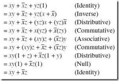
We can also use these identities to prove Boolean equalities. Suppose we want to prove that ![]()
The proof is given in Table 3.7.
Table 3-7: Example Using Identities
To prove the equality of two Boolean expressions, you can also create the truth tables for each and compare. If the truth tables are identical, the expressions are equal. We leave it as an exercise to find the truth tables for the equality in Table 3.7.
3.2.4 Complements
As you saw in Example 3.1, the Boolean identities can be applied to Boolean expressions, not simply Boolean variables (we treated xy as a Boolean variable and then applied the Idempotent Law). The same is true for the Boolean operators. The most common Boolean operator applied to more complex Boolean expressions is the NOT operator, resulting in the complement of the expression. Later we will see that there is a one-to-one correspondence between a Boolean function and its physical implementation using electronic circuits. Quite often, it is cheaper and less complicated to implement the complement of a function rather than the function itself. If we implement the complement, we must invert the final output to yield the original function; this is accomplished with one simple NOT operation. Therefore, complements are quite useful.
To find the complement of a Boolean function, we use DeMorgan’s Law. The OR form of this law states that![]()
. We can easily extend this to three or more variables as follows:
Given the function:
Let w = (x + y). Then
Now, applying DeMorgan’s Law again, we get:
Therefore, if F(x,y,z) = (x + y + z), then ![]() Applying the principle of duality, we see that
Applying the principle of duality, we see that ![]()
It appears that to find the complement of a Boolean expression, we simply replace each variable by its complement (x is replaced by ![]() and interchange ANDs and ORs. In fact, this is exactly what DeMorgan’s Law is telling us to do. For example, the complement of
and interchange ANDs and ORs. In fact, this is exactly what DeMorgan’s Law is telling us to do. For example, the complement of ![]() . We have to add the parentheses to ensure the correct precedence.
. We have to add the parentheses to ensure the correct precedence.
You can verify that this simple rule of thumb for finding the complement of a Boolean expression is correct by examining the truth tables for both the expression and its complement. The complement of any expression, when represented as a truth table, should have 0s for output everywhere the original function has 1s, and 1s in those places where the original function has 0s. Table 3.8 depicts the truth tables for ![]() and its complement,
and its complement, ![]() . The shaded portions indicate the final results for F and
. The shaded portions indicate the final results for F and ![]() .
.
Table 3-8: Truth Table Representation for a Function and Its Complement
3.2.5 Representing Boolean Functions
We have seen that there are many different ways to represent a given Boolean function. For example, we can use a truth table or we can use one of many different Boolean expressions. In fact, there are an infinite number of Boolean expressions that are logically equivalent to one another. Two expressions that can be represented by the same truth table are considered logically equivalent. See Example 3.4.
Example 3.4:
Suppose ![]() We can also express F as F(x,y,z) =
We can also express F as F(x,y,z) =![]() because the Idempotent Law tells us these two expressions are the same. We can also express F as
because the Idempotent Law tells us these two expressions are the same. We can also express F as ![]() using the Distributive Law.
using the Distributive Law.
![]()
To help eliminate potential confusion, logic designers specify a Boolean function using a canonical, or standardized, form. For any given Boolean function, there exists a unique standardized form. However, there are different “standards” that designers use. The two most common are the sum-of-products form and the product-of-sums form.
The sum-of-products form requires that the expression be a collection of ANDed variables (or product terms) that are ORed together. The function ![]() + xyz is in sum-of-products form. The function
+ xyz is in sum-of-products form. The function ![]() is not in sum-of-products form. We apply the Distributive Law to distribute the x variable in F2, resulting in the expression
is not in sum-of-products form. We apply the Distributive Law to distribute the x variable in F2, resulting in the expression ![]()
, which is now in sum-of-products form.
Boolean expressions stated in product-of-sums form consist of ORed variables (sum terms) that are ANDed together. The function F1(x,y,z) = (x + y)(x +![]()
is in product-of-sums form. The product-of-sums form is often preferred when the Boolean expression evaluates true in more cases than it evaluates false. This is not the case with the function, F1, so the sum-of-products form is appropriate. Also, the sum-of-products form is usually easier to work with and to simplify, so we use this form exclusively in the sections that follow.
Any Boolean expression can be represented in sum-of-products form. Because any Boolean expression can also be represented as a truth table, we conclude that any truth table can also be represented in sum-of-products form. It is a simple matter to convert a truth table into sum-of-products form, as indicated in the following example.
![]()
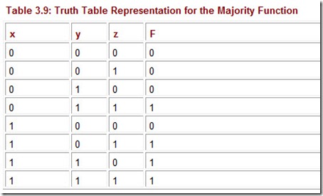
Consider a simple majority function. This is a function that, when given three inputs, outputs a 0 if less than half of its inputs are 1, and a 1 if at least half of its inputs are 1. Table 3.9 depicts the truth table for this majority function over three variables.
![]()
Table 3.9: Truth Table Representation for the Majority Function
To convert the truth table to sum-of-products form, we start by looking at the problem in reverse. If we want the expression x + y to equal 1, then either x or y (or both) must be equal to 1. If xy + yz = 1, then either xy = 1 or yz = 1 (or both). Using this logic in reverse and applying it to Example 3.5, we see that the function must output a 1 when x = 0, y = 1, and z = 1. The product term that satisfies this is ![]() (clearly this is equal to 1 when x = 0, y = 1, and z = 1). The second occurrence of an output value of 1 is when x = 1, y = 0, and z = 1. The product term to guarantee an output of 1 is
(clearly this is equal to 1 when x = 0, y = 1, and z = 1). The second occurrence of an output value of 1 is when x = 1, y = 0, and z = 1. The product term to guarantee an output of 1 is ![]() . The third product term we need is
. The third product term we need is ![]() , and the last is xyz. In summary, to generate a sum-of-products expression using the truth table for any Boolean expression, you must generate a product term of the input variables corresponding to each row where the value of the output variable in that row is 1. In each product term, you must then complement any variables that are 0 for that row.
, and the last is xyz. In summary, to generate a sum-of-products expression using the truth table for any Boolean expression, you must generate a product term of the input variables corresponding to each row where the value of the output variable in that row is 1. In each product term, you must then complement any variables that are 0 for that row.
Our majority function can be expressed in sum-of-products form as F(x,y,z) =![]() . Please note that this expression may not be in simplest form; we are only guaranteeing a standard form. The sum-of-products and product-of-sums standard forms are equivalent ways of expressing a Boolean function. One form can be converted to the other through an application of Boolean identities. Whether using sum-of-products or product-of-sums, the expression must eventually be converted to its simplest form, which means reducing the expression to the minimum number of terms. Why must the expressions be simplified? A one-to-one correspondence exists between a Boolean expression and its implementation using electrical circuits, as we shall see in the next section. Unnecessary product terms in the expression lead to unnecessary components in the physical circuit, which in turn yield a suboptimal circuit.
. Please note that this expression may not be in simplest form; we are only guaranteeing a standard form. The sum-of-products and product-of-sums standard forms are equivalent ways of expressing a Boolean function. One form can be converted to the other through an application of Boolean identities. Whether using sum-of-products or product-of-sums, the expression must eventually be converted to its simplest form, which means reducing the expression to the minimum number of terms. Why must the expressions be simplified? A one-to-one correspondence exists between a Boolean expression and its implementation using electrical circuits, as we shall see in the next section. Unnecessary product terms in the expression lead to unnecessary components in the physical circuit, which in turn yield a suboptimal circuit.
3.3 Logic Gates
The logical operators AND, OR, and NOT that we have discussed have been represented thus far in an abstract sense using truth tables and Boolean expressions. The actual physical components, or digital circuits, such as those that perform arithmetic operations or make choices in a computer, are constructed from a number of primitive elements called gates. Gates implement each of the basic logic functions we have discussed. These gates are the basic building blocks for digital design. Formally, a gate is a small, electronic device that computes various functions of two-valued signals. More simply stated, a gate implements a simple Boolean function. To physically implement each gate requires from one to six or more transistors (described in Chapters 1), depending on the technology being used. To summarize, the basic physical component of a computer is the transistor; the basic logic element is the gate.
3.3.1 Symbols for Logic Gates
We initially examine the three simplest gates. These correspond to the logical operators AND, OR, and NOT. We have discussed the functional behavior of each of these Boolean operators. Figure 3.1 depicts the graphical representation of the gate that corresponds to each operator.
Figure 3.1: The Three Basic Gates
Note the circle at the output of the NOT gate. Typically, this circle represents the complement operation.
Another common gate is the exclusive-OR (XOR) gate, represented by the Boolean expression: x Å y. XOR is false if both of the input values are equal and true otherwise. Figure 3.2 illustrates the truth table for XOR as well as the logic diagram that specifies its behavior.
Figure 3.2: a) The Truth Table for XOR. b) The Logic Symbol for XOR
3.3.2 Universal Gates
Two other common gates are NAND and NOR, which produce complementary output to AND and OR, respectively. Each gate has two different logic symbols that can be used for gate representation. (It is left as an exercise to prove that the symbols are logically equivalent. Hint: Use DeMorgan’s Law.) Figures 3.3 and 3.4 depict the logic diagrams for NAND and NOR along with the truth tables to explain the functional behavior of each gate.
Figure 3.3: The Truth Table and Logic Symbols for NAND
Figure 3.4: The Truth Table and Logic Symbols for NOR
The NAND gate is commonly referred to as a universal gate, because any electronic circuit can be constructed using only NAND gates. To prove this, Figure 3.5 depicts an AND gate, an OR gate, and a NOT gate using only NAND gates.
Figure 3.5: Three Circuits Constructed Using Only NAND Gates
Why not simply use the AND, OR, and NOT gates we already know exist? There are two reasons to investigate using only NAND gates to build any given circuit. First, NAND gates are cheaper to build than the other gates. Second, complex integrated circuits (which are discussed in the following sections) are often much easier to build using the same building block (i.e., several NAND gates) rather than a collection of the basic building blocks (i.e., a combination of AND, OR, and NOT gates).
Please note that the duality principle applies to universality as well. One can build any circuit using only NOR gates. NAND and NOR gates are related in much the same way as the sum-of-products form and the product-of-sums form presented earlier. One would use NAND for implementing an expression in sum-of-products form and NOR for those in product-of-sums form.
3.3.3 Multiple Input Gates
In our examples thus far, all gates have accepted only two inputs. Gates are not limited to two input values, however. There are many variations in the number and types of inputs and outputs allowed for various gates. For example, we can represent the expression x + y + z using one OR gate with three inputs, as in Figure 3.6.
Figure 3.6: A Three-Input OR Gate Representing x + y + z
Figure 3.7 represents the expression ![]()
Figure 3.7: A Three-Input AND Gate Representing
We shall see later in this chapter that it is sometimes useful to depict the output of a gate as Q along with its complement ![]() as shown in Figure 3.8.
as shown in Figure 3.8.
Figure 3.8: AND Gate with Two Inputs and Two Outputs
Note that Q always represents the actual output.
3.4 Digital Components
Upon opening a computer and looking inside, one would realize that there is a lot to know about all of the digital components that make up the system. Every computer is built using collections of gates that are all connected by way of wires acting as signal gateways. These collections of gates are often quite standard, resulting in a set of building blocks that can be used to build the entire computer system. Surprisingly, these building blocks are all constructed using the basic AND, OR, and NOT operations. In the next few sections, we discuss digital circuits, their relationship to Boolean algebra, the standard building blocks, and examples of the two different categories, combinational logic and sequential logic, into which these building blocks can be placed.
3.4.1 Digital Circuits and Their Relationship to Boolean Algebra
What is the connection between Boolean functions and digital circuits? We have seen that a simple Boolean operation (such as AND or OR) can be represented by a simple logic gate. More complex Boolean expressions can be represented as combinations of AND, OR, and NOT gates, resulting in a logic diagram that describes the entire expression. This logic diagram represents the physical implementation of the given expression, or the actual digital circuit. Consider the function
![]() (which we looked at earlier). Figure 3.9 represents a logic diagram that implements this function.
(which we looked at earlier). Figure 3.9 represents a logic diagram that implements this function.
We can build logic diagrams (which in turn lead to digital circuits) for any Boolean expression.
Boolean algebra allows us to analyze and design digital circuits. Because of the relationship between Boolean algebra and logic diagrams, we simplify our circuit by simplifying our Boolean expression. Digital circuits are implemented with gates, but gates and logic diagrams are not the most convenient forms for representing digital circuits during the design phase. Boolean expressions are much better to use during this phase because they are easier to manipulate and simplify.
The complexity of the expression representing a Boolean function has a direct impact on the complexity of the resulting digital circuit; the more complex the expression, the more complex the resulting circuit. We should point out that we do not typically simplify our circuits using Boolean identities; we have already seen that this can sometimes be quite difficult and time consuming. Instead, designers use a more automated method to do this. This method involves the use of Karnaugh maps (or Kmaps). The interested reader is referred to the focus section following this chapter to learn how Kmaps help to simplify digital circuits.
3.4.2 Integrated Circuits
Computers are composed of various digital components, connected by wires. Like a good program, the actual hardware of a computer uses collections of gates to create larger modules, which, in turn, are used to implement various functions. The number of gates required to create these “building blocks” depends on the technology being used. Because the circuit technology is beyond the scope of this text, the reader is referred to the reading list at the end of this chapter for more information on circuit technology.
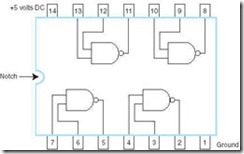
Typically, gates are not sold individually; they are sold in units called integrated circuits (ICs). A chip (a small silicon semiconductor crystal) is a small electronic device consisting of the necessary electronic components (transistors, resistors, and capacitors) to implement various gates. As described in Chapter 1, components are etched directly on the chip, allowing them to be smaller and to require less power for operation than their discrete component counterparts. This chip is then mounted in a ceramic or plastic container with external pins. The necessary connections are welded from the chip to the external pins to form an IC. The first ICs contained very few transistors. As we learned in Chapter 1, the first ICs were called SSI chips and contained up to 100 electronic components per chip. We now have ULSI (ultra large-scale integration) with more than 1 million electronic components per chip. Figure 3.10 illustrates a simple SSI IC.
Figure 3.10: A Simple SSI Integrated Circuit
3.5 Combinational Circuits
Digital logic chips are combined to give us useful circuits. These logic circuits can be categorized as either combinational logic or sequential logic. This section introduces combinational logic. Sequential logic is covered in Section 3.6.
3.5.1 Basic Concepts
Combinational logic is used to build circuits that contain basic Boolean operators, inputs, and outputs. The key concept in recognizing a combinational circuit is that an output is always based entirely on the given inputs. Thus, the output of a combinational circuit is a function of its inputs, and the output is uniquely determined by the values of the inputs at any given moment. A given combinational circuit may have several outputs. If so, each output represents a different Boolean function.
3.5.2 Examples of Typical Combinational Circuits
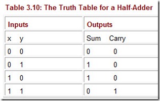
Let’s begin with a very simple combinational circuit called a half-adder. Consider the problem of adding two binary digits together. There are only three things to remember: 0 + 0 = 0, 0 + 1 = 1 + 0 = 1, and 1 + 1 = 10. We know the behavior this circuit exhibits, and we can formalize this behavior using a truth table. We need to specify two outputs, not just one, because we have a sum and a carry to address. The truth table for a half-adder is shown in Table 3.10.
Table 3.10: The Truth Table for a Half-Adder
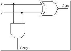
A closer look reveals that Sum is actually an XOR. The Carry output is equivalent to that of an AND gate. We can combine an XOR gate and an AND gate, resulting in the logic diagram for a half-adder shown in Figure 3.11.
Figure 3.11: The Logic Diagram for a Half-Adder
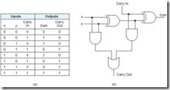
The half-adder is a very simple circuit and not really very useful because it can only add two bits together. However, we can extend this adder to a circuit that allows the addition of larger binary numbers. Consider how you add base 10 numbers: You add up the rightmost column, note the units digit, and carry the tens digit. Then you add that carry to the current column, and continue in a similar fashion. We can add binary numbers in the same way. However, we need a circuit that allows three inputs (x, y, and Carry In), and two outputs (Sum and Carry Out). Figure 3.12 illustrates the truth table and corresponding logic diagram for a full-adder. Note that this full-adder is composed of two half-adders and an OR gate.
Figure 3.12: a) A Truth Table for a Full-Adder. b) A Logic Diagram for a Full-Adder
Given this full-adder, you may be wondering how this circuit can add binary numbers, since it is capable of adding only three bits. The answer is, it can’t. However, we can build an adder capable of adding two 16-bit words, for example, by replicating the above circuit 16 times, feeding the Carry Out of one circuit into the Carry In of the circuit immediately to its left. Figure 3.13 illustrates this idea. This type of circuit is called a ripple-carry adder because of the sequential generation of carries that “ripple” through the adder stages. Note that instead of drawing all the gates that constitute a full-adder, we use a black box approach to depict our adder. A black box approach allows us to ignore the details of the actual gates. We concern ourselves only with the inputs and outputs of the circuit. This is typically done with most circuits, including decoders, multiplexers, and adders, as we shall see very soon.
Figure 3.13: The Logic Diagram for a Ripple-Carry Adder
Because this adder is very slow, it is not normally implemented. However, it is easy to understand and should give you some idea of how addition of larger binary numbers can be achieved. Modifications made to adder designs have resulted in the carry-look-ahead adder, the carry-select adder, and the carry-save adder, as well as others. Each attempts to shorten the delay required to add two binary numbers. In fact, these newer adders achieve speeds 40% to 90% faster than the ripple-carry adder by performing additions in parallel and reducing the maximum carry path.
Adders are very important circuits—a computer would not be very useful if it could not add numbers. An equally important operation that all computers use frequently is decoding binary information from a set of n inputs to a maximum of 2n outputs. A decoder uses the inputs and their respective values to select one specific output line. What do we mean by “select an output line”? It simply means that one unique output line is asserted, or set to 1, while the other output lines are set to zero. Decoders are normally defined by the number of inputs and the number of outputs. For example, a decoder that has 3 inputs and 8 outputs is called a 3-to-8 decoder.
We mentioned that this decoder is something the computer uses frequently. At this point, you can probably name many arithmetic operations the computer must be able to perform, but you might find it difficult to propose an example of decoding. If so, it is because you are not familiar with how a computer accesses memory.
All memory addresses in a computer are specified as binary numbers. When a memory address is referenced (whether for reading or for writing), the computer first has to determine the actual address. This is done using a decoder. The following example should clarify any questions you may have about how a decoder works and what it might be used for.
![]()
Imagine memory consisting of 8 chips, each containing 8K bytes. Let’s assume chip 0 contains memory addresses 0–8191, chip 1 contains memory addresses 8192–16,383, and so on. We have a total of 8K x 8, or 64K (65,536) addresses available. We will not write down all 64K addresses as binary numbers; however, writing a few addresses in binary form (as we illustrate in the following paragraphs) will illustrate why a decoder is necessary.
Given 64 = 26 and 1K = 210, then 64K = 26 x 210 = 216, which indicates we need 16 bits to represent each address. If you have trouble understanding this, start with a smaller number of addresses. For example, if you have 4 addresses—addresses 0, 1, 2, and 3, the binary equivalent of these addresses is 00, 01, 10, and 11, requiring two bits. We know 22 = 4. Now consider eight addresses. We have to be able to count from 0 to 7 in binary. How many bits does that require? The answer is 3. You can either write them all down, or you recognize that 8 = 23. The exponent tells us the minimum number of bits necessary to represent the addresses.
All addresses on chip 0 have the format: 000xxxxxxxxxxxxx. Because chip 0 contains the addresses 0–8191, the binary representation of these addresses is in the range 0000000000000000 to 0001111111111111. Similarly, all addresses on chip 1 have the format 001xxxxxxxxxxxxx, and so on for the remaining chips. The leftmost 3 bits determine on which chip the address is actually located. We need 16 bits to represent the entire address, but on each chip, we only have 213 addresses. Therefore, we need only 13 bits to uniquely identify an address on a given chip. The rightmost 13 bits give us this information.
When a computer is given an address, it must first determine which chip to use; then it must find the actual address on that specific chip. In our example, the computer would use the 3 leftmost bits to pick the chip and then find the address on the chip using the remaining 13 bits. These 3 high-order bits are actually used as the inputs to a decoder so the computer can determine which chip to activate for reading or writing. If the first 3 bits are 000, chip 0 should be activated. If the first 3 bits are 111, chip 7 should be activated. Which chip would be activated if the first 3 bits were 010? It would be chip 2. Turning on a specific wire activates a chip. The output of the decoder is used to activate one, and only one, chip as the addresses are decoded.
![]()
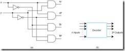
Figure 3.14 illustrates the physical components in a decoder and the symbol often used to represent a decoder. We will see how a decoder is used in memory in Section 3.6.
Figure 3.14: a) A Look Inside a Decoder. b) A Decoder Symbol
Another common combinational circuit is a multiplexer. This circuit selects binary information from one of many input lines and directs it to a single output line. Selection of a particular input line is controlled by a set of selection variables, or control lines. At any given time, only one input (the one selected) is routed through the circuit to the output line. All other inputs are “cut off.” If the values on the control lines change, the input actually routed through changes as well. Figure 3.15 illustrates the physical components in a multiplexer and the symbol often used to represent a multiplexer.
Figure 3.15: a) A Look Inside a Multiplexer. b) A Multiplexer Symbol
Can you think of some situations that require multiplexers? Time-sharing computers multiplex the input from user terminals. Modem pools multiplex the modem lines entering the computer.
Another useful set of combinational circuits to study includes a parity generator and a parity checker (recall we studied parity in Chapter 2). A parity generator is a circuit that creates the necessary parity bit to add to a word; a parity checker checks to make sure proper parity (odd or even) is present in the word, detecting an error if the parity bit is incorrect.
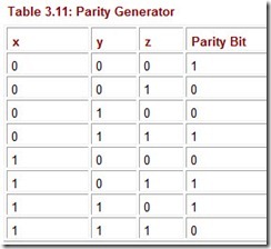
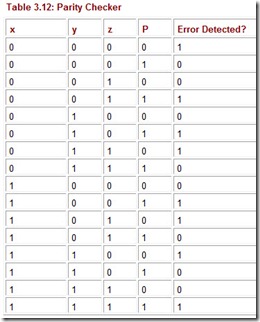
Typically parity generators and parity checkers are constructed using XOR functions. Assuming we are using odd parity, the truth table for a parity generator for a 3-bit word is given in Table 3.11. The truth table for a parity checker to be used on a 4-bit word with 3 information bits and 1 parity bit is given in Table 3.12. The parity checker outputs a 1 if an error is detected and 0 otherwise. We leave it as an exercise to draw the corresponding logic diagrams for both the parity generator and the parity checker.
Table 3.12: Parity Checker
There are far too many combinational circuits for us to be able to cover them all in this brief chapter. Comparators, shifters, programmable logic devices—these are all valuable circuits and actually quite easy to understand. The interested reader is referred to the references at the end of this chapter for more information on combinational circuits. However, before we finish the topic of combinational logic, there is one more combinational circuit we need to introduce. We have covered all of the components necessary to build an arithmetic logic unit (ALU).
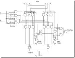
Figure 3.16 illustrates a very simple ALU with four basic operations—AND, OR, NOT, and addition—carried out on two machine words of 2 bits each. The control lines, f0 and f1, determine which operation is to be performed by the CPU. The signal 00 is used for addition (A + B); 01 for NOT A; 10 for A OR B, and 11 for A AND B. The input lines A0 and A1 indicate 2 bits of one word, while B0 and B1 indicate the second word. C0 and C1 represent the output lines.
Figure 3.16: A Simple Two-Bit ALU
3.6 Sequential Circuits
In the previous section we studied combinational logic. We have approached our study of Boolean functions by examining the variables, the values for those variables, and the function outputs that depend solely on the values of the inputs to the functions. If we change an input value, this has a direct and immediate impact on the value of the output. The major weakness of combinational circuits is that there is no concept of storage-they are memoryless. This presents us with a bit of a dilemma. We know that computers must have a way to remember values. Consider a much simpler digital circuit needed for a soda machine. When you put money into a soda machine, the machine remembers how much you have put in at any given instant. Without this ability to remember, it would be very difficult to use. A soda machine cannot be built using only combinational circuits. To understand how a soda machine works, and ultimately how a computer works, we must study sequential logic.
3.6.1 Basic Concepts
A sequential circuit defines its output as a function of both its current inputs and its previous inputs. Therefore, the output depends on past inputs. To remember previous inputs, sequential circuits must have some sort of storage element. We typically refer to this storage element as a flip-flop. The state of this flip-flop is a function of the previous inputs to the circuit. Therefore, pending output depends on both the current inputs and the current state of the circuit. In the same way that combinational circuits are generalizations of gates, sequential circuits are generalizations of flip-flops.
3.6.2 Clocks
Before we discuss sequential logic, we must first introduce a way to order events. (The fact that a sequential circuit uses past inputs to determine present outputs indicates we must have event ordering.) Some sequential circuits are asynchronous, which means they become active the moment any input value changes. Synchronous sequential circuits use clocks to order events. A clock is a circuit that emits a series of pulses with a precise pulse width and a precise interval between consecutive pulses. This interval is called the clock cycle time. Clock speed is generally measured in megahertz (MHz), or millions of pulses per second. Common cycle times are from one to several hundred MHz.
A clock is used by a sequential circuit to decide when to update the state of the circuit (when do “present” inputs become “past” inputs?). This means that inputs to the circuit can only affect the storage element at given, discrete instances of time. In this chapter we examine synchronous sequential circuits because they are easier to understand than their asynchronous counterparts. From this point, when we refer to “sequential circuit“, we are implying “synchronous sequential circuit.”
Most sequential circuits are edge-triggered (as opposed to being level-triggered). This means they are allowed to change their states on either the rising or falling edge of the clock signal, as seen in Figure 3.17.
Figure 3.17: A Clock Signal Indicating Discrete Instances of Time
3.6.3 Flip-Flops
A level-triggered circuit is allowed to change state whenever the clock signal is either high or low. Many people use the terms latch and flip-flop interchangeably. Technically, a latch is level triggered, whereas a flip-flop is edge triggered. In this book, we use the term flip-flop.
In order to “remember” a past state, sequential circuits rely on a concept called feedback. This simply means the output of a circuit is fed back as an input to the same circuit. A very simple feedback circuit uses two NOT gates, as shown in Figure 3.18.
Figure 3.18: Example of Simple Feedback
In this figure, if Q is 0, it will always be 0. If Q is 1, it will always be 1. This is not a very interesting or useful circuit, but it allows you to see how feedback works.
A more useful feedback circuit is composed of two NOR gates resulting in the most basic memory unit called an SR flip-flop. SR stands for “set/reset.” The logic diagram for the SR flip-flop is given in Figure 3.19.
Figure 3.19: An SR Flip-Flop Logic Diagram
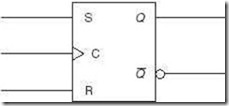
We can describe any flip-flop by using a characteristic table, which indicates what the next state should be based on the inputs and the current state, Q. The notation Q(t) represents the current state, and Q(t + 1) indicates the next state, or the state the flip-flop should enter after the clock has been pulsed. Figure 3.20 shows the actual implementation of the SR sequential circuit and its characteristic table.
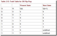
An SR flip-flop exhibits interesting behavior. There are three inputs: S, R, and the current output Q(t). We create the truth table shown in Table 3.13 to illustrate how this circuit works.
Table 3.13: Truth Table for SR Flip-Flop
For example, if S is 0 and R is 0, and the current state, Q(t), is 0, then the next state, Q(t + 1), is also 0. If S is 0 and R is 0, and Q(t) is 1, then Q(t+1) is 1. Actual inputs of (0,0) for (S,R) result in no change when the clock is pulsed. Following a similar argument, we can see that inputs (S,R) = (0,1) force the next state, Q(t + 1), to 0 regardless of the current state (thus forcing a reset on the circuit output). When (S,R) = (1,0), the circuit output is set to 1.
There is one oddity with this particular flip-flop. What happens if both S and R are set to 1 at the same time? This forces both Q and ![]() to 1, but how can Q = 1 =
to 1, but how can Q = 1 = ![]() ? This results in an unstable circuit. Therefore, this combination of inputs is not allowed in an SR flip-flop.
? This results in an unstable circuit. Therefore, this combination of inputs is not allowed in an SR flip-flop.
We can add some conditioning logic to our SR flip-flop to ensure that the illegal state never arises-we simply modify the SR flip-flop as shown in Figure 3.21. This results in a JK flip-flop. JK flip-flops were named after the Texas Instruments engineer, Jack Kilby, who invented the integrated circuit in 1958.
Figure 3.21: a) A JK Flip-Flop.
b) The JK Characteristic Table.
c) A JK Flip-Flop as a Modified SR Flip-Flop
Another variant of the SR flip-flop is the D (data) flip-flop. A D flip-flop is a true representation of physical computer memory. This sequential circuit stores one bit of information. If a 1 is asserted on the input line D, and the clock is pulsed, the output line Q becomes a 1. If a 0 is asserted on the input line and the clock is pulsed, the output becomes 0. Remember that output Q represents the current state of the circuit. Therefore, an output value of 1 means the circuit is currently “storing” a value of 1. Figure 3.22 illustrates the D flip-flop, lists its characteristic table, and reveals that the D flip-flop is actually a modified SR flip-flop.
Figure 3.22: a) A D Flip-Flop.
b) The D Characteristic Table.
c) A D Flip-Flop as a Modified SR Flip-Flop
3.6.4 Examples of Sequential Circuits
Latches and flip-flops are used to implement more complex sequential circuits. Registers, counters, memories, and shift registers all require the use of storage, and are therefore implemented using sequential logic.
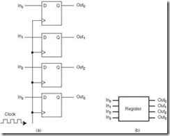
Our first example of a sequential circuit is a simple 4-bit register implemented using four D flip-flops. (To implement registers for larger words, we would simply need to add flip-flops.) There are four input lines, four output lines, and a clock signal line. The clock is very important from a timing standpoint; the registers must all accept their new input values and change their storage elements at the same time. Remember that a synchronous sequential circuit cannot change state unless the clock pulses. The same clock signal is tied into all four D flip-flops, so they change in unison. Figure 3.23 depicts the logic diagram for our 4-bit register, as well as a block diagram for the register. In reality, physical components have additional lines for power and for ground, as well as a clear line (which gives the ability to reset the entire register to all zeros). However, in this text, we are willing to leave those concepts to the computer engineers and focus on the actual digital logic present in these circuits.
Figure 3.23: a) A 4-Bit Register.
b) A Block Diagram for a 4-Bit Register
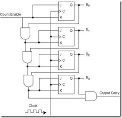
Another useful sequential circuit is a binary counter, which goes through a predetermined sequence of states as the clock pulses. In a straight binary counter, these states reflect the binary number sequence. If we begin counting in binary: 0000, 0001, 0010, 0011, . . . , we can see that as the numbers increase, the low-order bit is complemented each time. Whenever it changes state from 1 to 0, the bit to the left is then complemented. Each of the other bits changes state from 0 to 1 when all bits to the right are equal to 1. Because of this concept of complementing states, our binary counter is best implemented using a JK flip-flop (recall that when J and K are both equal to 1, the flip-flop complements the present state). Instead of independent inputs to each flip-flop, there is a count enable line that runs to each flip-flop. The circuit counts only when the clock pulses and this count enable line is set to 1. If count enable is set to 0 and the clock pulses, the circuit does not change state. You should examine Figure 3.24 very carefully, tracing the circuit with various inputs to make sure you understand how this circuit outputs the binary numbers from 0000 to 1111. You should also check to see which state the circuit enters if the current state is 1111 and the clock is pulsed.
Figure 3.24: A 4-Bit Synchronous Counter Using JK Flip-Flops
We have looked at a simple register and a binary counter. We are now ready to examine a very simple memory circuit.
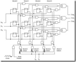
The memory depicted in Figure 3.25 holds four 3-bit words (this is typically denoted as a 4 x 3 memory). Each column in the circuit represents one 3-bit word. Notice that the flip-flops storing the bits for each word are synchronized via the clock signal, so a read or write operation always reads or writes a complete word. The inputs In0, In1, and In2 are the lines used to store, or write, a 3-bit word to memory. The lines S0 and S1 are the address lines used to select which word in memory is being referenced. (Notice that S0 and S1 are the input lines to a 2-to-4 decoder that is responsible for selecting the correct memory word.) The three output lines (Out1,Out2, and Out3) are used when reading words from memory.
Figure 3.25: A 4 x 3 Memory
You should notice another control line as well. The write enable control line indicates whether we are reading or writing. Note that in this chip, we have separated the input and output lines for ease of understanding. In practice, the input lines and output lines are the same lines.
To summarize our discussion of this memory circuit, here are the steps necessary to write a word to memory:
-
An address is asserted on S0 and S1.
-
WE (write enable) is set to high.
-
The decoder using S0 and S1 enables only one AND gate, selecting a given word in memory.
-
The line selected in Step 3 combined with the clock and WE select only one word.
-
The write gate enabled in Step 4 drives the clock for the selected word.
-
When the clock pulses, the word on the input lines is loaded into the D flip-flops.
We leave it as an exercise to create a similar list of the steps necessary to read a word from this memory. Another interesting exercise is to analyze this circuit and determine what additional components would be necessary to extend the memory from, say, a 4 x 3 memory to an 8 x 3 memory or a 4 x 8 memory.
3.7 Designing Circuits
In the preceding sections, we introduced many different components used in computer systems. We have, by no means, provided enough detail to allow you to start designing circuits or systems. Digital logic design requires someone not only familiar with digital logic, but also well versed in digital analysis (analyzing the relationship between inputs and outputs), digital synthesis (starting with a truth table and determining the logic diagram to implement the given logic function), and the use of CAD (computer-aided design) software. Recall from our previous discussions that great care needs to be taken when designing the circuits to ensure that they are minimized. A circuit designer faces many problems, including finding efficient Boolean functions, using the smallest number of gates, using an inexpensive combination of gates, organizing the gates of a circuit board to use the smallest surface area and minimal power requirements, and attempting to do all of this using a standard set of modules for implementation. Add to this the many problems we have not discussed, such as signal propagation, fan out, synchronization issues, and external interfacing, and you can see that digital circuit design is quite complicated.
Up to this point, we have discussed how to design registers, counters, memory, and various other digital building blocks. Given these components, a circuit designer can implement any given algorithm in hardware (recall the Principle of Equivalence of Hardware and Software from Chapter 1). When you write a program, you are specifying a sequence of Boolean expressions. Typically, it is much easier to write a program than it is to design the hardware necessary to implement the algorithm. However, there are situations in which the hardware implementation is better (for example, in a real-time system, the hardware implementation is faster, and faster is definitely better.) However, there are also cases in which a software implementation is better. It is often desirable to replace a large number of digital components with a single programmed microcomputer chip, resulting in an embedded system. Your microwave oven and your car most likely contain embedded systems. This is done to replace additional hardware that could present mechanical problems. Programming these embedded systems requires design software that can read input variables and send output signals to perform such tasks as turning a light on or off, emitting a beep, sounding an alarm, or opening a door. Writing this software requires an understanding of how Boolean functions behave.
Chapter Summary
The main purpose of this chapter is to acquaint you with the basic concepts involved in logic design and to give you a general understanding of the basic circuit configurations used to construct computer systems. This level of familiarity will not enable you to design these components; rather, it gives you a much better understanding of the architectural concepts discussed in the following chapters.
In this chapter we examined the behaviors of the standard logical operators AND, OR, and NOT and looked at the logic gates that implement them. Any Boolean function can be represented as a truth table, which can then be transformed into a logic diagram, indicating the components necessary to implement the digital circuit for that function. Thus, truth tables provide us with a means to express the characteristics of Boolean functions as well as logic circuits. In practice, these simple logic circuits are combined to create components such as adders, ALUs, decoders, multiplexers, registers, and memory.
There is a one-to-one correspondence between a Boolean function and its digital representation. Boolean identities can be used to reduce Boolean expressions, and thus, to minimize both combinational and sequential circuits. Minimization is extremely important in circuit design. From a chip designer’s point of view, the two most important factors are speed and cost: minimizing the circuits helps to both lower the cost and increase performance.
Digital logic is divided into two categories: combinational logic and sequential logic. Combinational logic devices, such as adders, decoders, and multiplexers, produce outputs that are based strictly on the current inputs. The AND, OR, and NOT gates are the building blocks for combinational logic circuits, although universal gates, such as NAND and NOR, could also be used. Sequential logic devices, such as registers, counters, and memory, produce outputs based on the combination of current inputs and the current state of the circuit. These circuits are built using SR, D, and JK flip-flops.
These logic circuits are the building blocks necessary for computer systems. In the next chapter we put these blocks together and take a closer, more detailed look at how a computer actually functions.
If you are interested in learning more about Kmaps, there is a special section that focuses on Kmaps located at the end of this chapter, after the exercises.
Review of Essential Terms and Concepts
-
Why is an understanding of Boolean algebra important to computer scientists?
-
Which Boolean operation is referred to as a Boolean product?
-
Which Boolean operation is referred to as a Boolean sum?
-
Create truth tables for the Boolean operators OR, AND, and NOT.
-
What is the Boolean duality principle?
-
Why is it important for Boolean expressions to be minimized in the design of digital circuits?
-
What is the relationship between transistors and gates?
-
Name the four basic logic gates.
-
What are the two universal gates described in this chapter? Why are these universal gates important?
-
Describe the basic construction of a digital logic chip.
-
Describe the operation of a ripple-carry adder. Why are ripple-carry adders not used in most computers today?
-
What do we call a circuit that takes several inputs and their respective values to select one specific output line? Name one important application for these devices.
-
What kind of circuit selects binary information from one of many input lines and directs it to a single output line?
-
How are sequential circuits different from combinational circuits?
-
What is the basic element of a sequential circuit?
-
What do we mean when we say that a sequential circuit is edge-triggered rather than level-triggered?
-
What is feedback?
-
How is a JK flip-flop related to an SR flip-flop?
-
Why are JK flip-flops often preferred to SR flip-flops?
-
Which flip-flop gives a true representation of computer memory?
Exercises
-
Hints and Answer Construct a truth table for the following: a. Hints and Answer
 b.Hints and Answer
-
Hints and Answer Using DeMorgan’s Law, write an expression for the complement of F if F(x,y,z) =
 .
. -
Using DeMorgan’s Law, write an expression for the complement of F if F(x,y,z) = xy +
 .
. -
Hints and Answer Using DeMorgan’s Law, write an expression for the complement of F if F(w,x,y,z) =
 .
. -
Use the Boolean identities to prove the following: a.The absorption laws b.DeMorgan’s laws
-
Hints and Answer Is the following distributive law valid or invalid? Prove your answer. x XOR (y AND z) = (x XOR y) AND (x XOR z)
-
Show that
 a.Using truth tables b.Hints and Answer Using Boolean identities
 -
Simplify the following functional expressions using Boolean algebra and its identities. List the identity used at each step. a.
 b.
b. c.
c.
-
Simplify the following functional expressions using Boolean algebra and its identities. List the identity used at each step. a.Hints and Answer
 b.Hints and Answer
  c.Hints and Answer
-
Simplify the following functional expressions using Boolean algebra and its identities. List the identity used at each step. a. (ab + c + df)ef b. x + xy c.
-
Simplify the following functional expressions using Boolean algebra and its identities. List the identity used at each step. a.Hints and Answer xy + x b. yz + xz c. wx + w(xy + y)
-
Hints and Answer Using the basic identities of Boolean algebra, show that: x( + y) = xy
-
Asterisk Mark Using the basic identities of Boolean algebra, show that: x + y = x + y
-
Hints and Answer Using the basic identities of Boolean algebra, show that: xy + z + yz = xy + z
-
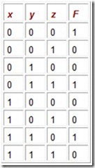
Hints and Answer The truth table for a Boolean expression is shown below. Write the Boolean expression in sum-of-products form.
-
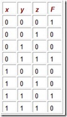
The truth table for a Boolean expression is shown below. Write the Boolean expression in sum-of-products form.
-
Draw the truth table and rewrite the expression below as the complemented sum of two products:

-
Given the Boolean function
 a. Hints and Answer Derive an algebraic expression for the complement of F. Express in sum-of-products form. b. Show that
  . c.Show that
  .
. -
Given the function
 a. List the truth table for F. b.Draw the logic diagram using the original Boolean expression. c.Simplify the expression using Boolean algebra and identities. d.List the truth table for your answer in Part c. e.Draw the logic diagram for the simplified expression in Part c.
 -
Construct the XOR operator using only AND, OR, and NOT gates.
-
Asterisk Mark Construct the XOR operator using only NAND gates.

-
Design a circuit with three inputs (x,y, and z) representing the bits in a binary number, and three outputs (a,b, and c) also representing bits in a binary number. When the input is 0, 1, 2, or 3, the binary output should be one less than the input. When the binary input is 4, 5, 6, or 7, the binary output should be one greater than the input. Show your truth table, all computations for simplification, and the final circuit.
-
Draw the combinational circuit that directly implements the following Boolean expression:

-
Hints and Answer Draw the combinational circuit that directly implements the following Boolean expression:

-
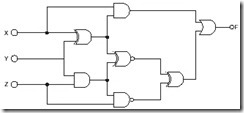
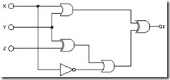
Hints and Answer Find the truth table that describes the following circuit:
-
Draw circuits to implement the parity generator and parity checker shown in Tables 3.11 and 3.12, respectively.
-
Draw a half-adder using only NAND gates.
-
Draw a full-adder using only NAND gates.
-
Tyrone Shoelaces has invested a huge amount of money into the stock market and doesn’t trust just anyone to give him buying and selling information. Before he will buy a certain stock, he must get input from three sources. His first source is Pain Webster, a famous stock broker. His second source is Meg A. Cash, a self-made millionaire in the stock market, and his third source is Madame LaZora, a world-famous psychic. After several months of receiving advice from all three, he has come to the following conclusions: a.Buy if Pain and Meg both say yes and the psychic says no. b.Buy if the psychic says yes. c.Don’t buy otherwise.
Construct a truth table and find the minimized Boolean function to implement the logic telling Tyrone when to buy.
35. Hints and Answer Asterish Mark A very small company has hired you to install a security system. The brand of system that you install is priced by the number of bits encoded on the proximity cards that allow access to certain locations in a facility. Of course, this small company wants to use the fewest bits possible (spending the least amount of money as possible) yet have all of their security needs met. The first thing you need to do is determine how many bits each card requires. Next, you have to program card readers in each secured location so that they respond appropriately to a scanned card.
This company has four types of employees and five areas that they wish to restrict to certain employees. The employees and their restrictions are as follows: a. The Big Boss needs access to the executive lounge and the executive washroom. b.The Big Boss’s secretary needs access to the supply closet, employee lounge, and executive lounge. c.Computer room employees need access to the server room and the employee lounge. d.The janitor needs access to all areas in the workplace.
Determine how each class of employee will be encoded on the cards and construct logic diagrams for the card readers in each of the five restricted areas.
36. How many 256 x 8 RAM chips are needed to provide a memory capacity of 4096 bytes? a.How many bits will each memory address contain? b.How many address lines must go to each chip? c.How many lines must be decoded for the chip select inputs? Specify the size of the decoder.
37.Hints and Answer Asterish Mark Investigate the operation of the following circuit. Assume an initial state of 0000. Trace the outputs (the Qs) as the clock ticks and determine the purpose of the circuit. You must show the trace to complete your answer.
38.Describe how each of the following circuits works and indicate typical inputs and outputs. Also provide a carefully labeled black box diagram for each. a.coder b.ltiplexer
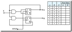
39.Hints and Answer Complete the truth table for the following sequential circuit:
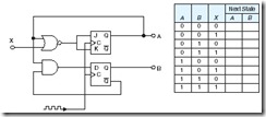
40.Complete the truth table for the following sequential circuit:
41.Hints and Answer Complete the truth table for the following sequential circuit:
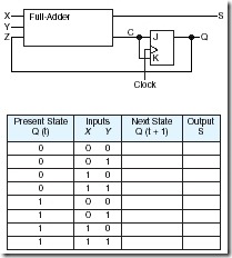
42.A sequential circuit has one flip-flop; two inputs, X and Y; and one output, S. It consists of a full-adder circuit connected to a D flip-flop, as shown below. Fill in the characteristic table for this sequential circuit by completing the Next State and Output columns.
43.Hints and Answer Asterish Mark A Mux-Not flip-flop (MN flip-flop) behaves as follows: If M = 1, the flip-flop complements the current state. If M = 0, the next state of the flip-flop is equal to the value of N. a.Derive the characteristic table for the flip-flop. b.Show how a JK flip-flop can be converted to an MN flip-flop by adding gate(s) and inverter(s).
44.Hints and Answer List the steps necessary to read a word from memory in the 4 x 3 memory circuit shown in Figure 3.25.
