Chapter 4: MARIE — An Introduction to a Simple Computer
4.1 Introduction
“When you wish to produce a result by means of an instrument, do not allow yourself to complicate it.”
—Leonardo da Vinci
Designing a computer nowadays is a job for a computer engineer with plenty of training. It is impossible in an introductory textbook such as this (and in an introductory course in computer organization and architecture) to present everything necessary to design and build a working computer such as those we can buy today. However, in this chapter, we first look at a very simple computer called MARIE: A Machine Architecture that is Really Intuitive and Easy. We then provide brief overviews of Intel and MIPs machines, two popular architectures reflecting the CISC and RISC design philosophies. The objective of this chapter is to give you an understanding of how a computer functions. We have, therefore, kept the architecture as uncomplicated as possible, following the advice in the opening quote by Leonardo da Vinci.
4.1.1 CPU Basics and Organization
From our studies in Chapter 2 (data representation) we know that a computer must manipulate binary-coded data. We also know from Chapter 3 that memory is used to store both data and program instructions (also in binary). Somehow, the program must be executed and the data must be processed correctly. The central processing unit (CPU) is responsible for fetching program instructions, decoding each instruction that is fetched, and performing the indicated sequence of operations on the correct data. To understand how computers work, you must first become familiar with their various components and the interaction among these components. To introduce the simple architecture in the next section, we first examine, in general, the microarchitecture that exists at the control level of modern computers.
All computers have a central processing unit. This unit can be divided into two pieces. The first is the datapath, which is a network of storage units (registers) and arithmetic and logic units (for performing various operations on data) connected by buses (capable of moving data from place to place) where the timing is controlled by clocks. The second CPU component is the control unit, a module responsible for sequencing operations and making sure the correct data is where it needs to be at the correct time. Together, these components perform the tasks of the CPU: fetching instructions, decoding them, and finally performing the indicated sequence of operations. The performance of a machine is directly affected by the design of the datapath and the control unit. Therefore, we cover these components of the CPU in detail in the following sections.
The Registers
Registers are used in computer systems as places to store a wide variety of data, such as addresses, program counters, or data necessary for program execution. Put simply, a register is a hardware device that stores binary data. Registers are located on the processor so information can be accessed very quickly. We saw in Chapter 3 that D flip-flops can be used to implement registers. One D flip-flop is equivalent to a 1-bit register, so a collection of D flip-flops is necessary to store multi-bit values. For example, to build a 16-bit register, we need to connect 16 D flip-flops together. We saw in our binary counter figure from Chapter 3 that these collections of flip-flops must be clocked to work in unison. At each pulse of the clock, input enters the register and cannot be changed (and thus is stored) until the clock pulses again.
Data processing on a computer is usually done on fixed size binary words that are stored in registers. Therefore, most computers have registers of a certain size. Common sizes include 16, 32, and 64 bits. The number of registers in a machine varies from architecture to architecture, but is typically a power of 2, with 16 and 32 being most common. Registers contain data, addresses, or control information. Some registers are specified as “special purpose” and may contain only data, only addresses, or only control information. Other registers are more generic and may hold data, addresses, and control information at various times.
Information is written to registers, read from registers, and transferred from register to register. Registers are not addressed in the same way memory is addressed (recall that each memory word has a unique binary address beginning with location 0). Registers are addressed and manipulated by the control unit itself.
In modern computer systems, there are many types of specialized registers: registers to store information, registers to shift values, registers to compare values, and registers that count. There are “scratchpad” registers that store temporary values, index registers to control program looping, stack pointer registers to manage stacks of information for processes, status registers to hold the status or mode of operation (such as overflow, carry, or zero conditions), and general purpose registers that are the registers available to the programmer. Most computers have register sets, and each set is used in a specific way. For example, the Pentium architecture has a data register set and an address register set. Certain architectures have very large sets of registers that can be used in quite novel ways to speed up execution of instructions. (We discuss this topic when we cover advanced architectures in Chapter 9.)
The ALU
The arithmetic logic unit (ALU) carries out the logic operations (such as comparisons) and arithmetic operations (such as add or multiply) required during the program execution. You saw an example of a simple ALU in Chapter 3. Generally an ALU has two data inputs and one data output. Operations performed in the ALU often affect bits in the status register (bits are set to indicate actions such as whether an overflow has occurred). The ALU knows which operations to perform because it is controlled by signals from the control unit.
The Control Unit
The control unit is the “policeman” or “traffic manager” of the CPU. It monitors the execution of all instructions and the transfer of all information. The control unit extracts instructions from memory, decodes these instructions, making sure data is in the right place at the right time, tells the ALU which registers to use, services interrupts, and turns on the correct circuitry in the ALU for the execution of the desired operation. The control unit uses a program counter register to find the next instruction for execution and a status register to keep track of overflows, carries, borrows, and the like. Section 4.7 covers the control unit in more detail.
4.1.2 The Bus
The CPU communicates with the other components via a bus. A bus is a set of wires that acts as a shared but common data path to connect multiple subsystems within the system. It consists of multiple lines, allowing the parallel movement of bits. Buses are low cost but very versatile, and they make it easy to connect new devices to each other and to the system. At any one time, only one device (be it a register, the ALU, memory, or some other component) may use the bus. However, this sharing often results in a communications bottleneck. The speed of the bus is affected by its length as well as by the number of devices sharing it. Quite often, devices are divided into master and slave categories, where a master device is one that initiates actions and a slave is one that responds to requests by a master.
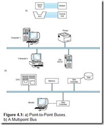
A bus can be point-to-point, connecting two specific components (as seen in Figure 4.1a) or it can be a common pathway that connects a number of devices, requiring these devices to share the bus (referred to as a multipoint bus and shown in Figure 4.1b).
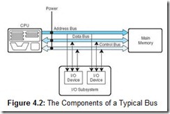
Because of this sharing, the bus protocol (set of usage rules) is very important. Figure 4.2 shows a typical bus consisting of data lines, address lines, control lines, and power lines. Often the lines of a bus dedicated to moving data are called the data bus. These data lines contain the actual information that must be moved from one location to another. Control lines indicate which device has permission to use the bus and for what purpose (reading or writing from memory or from an I/O device, for example). Control lines also transfer acknowledgments for bus requests, interrupts, and clock synchronization signals. Address lines indicate the location (in memory, for example) that the data should be either read from or written to. The power lines provide the electrical power necessary. Typical bus transactions include sending an address (for a read or write), transferring data from memory to a register (a memory read), and transferring data to the memory from a register (a memory write). In addition, buses are used for I/O reads and writes from peripheral devices. Each type of transfer occurs within a bus cycle, the time between two ticks of the bus clock.
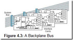
Due to the different types of information buses transport and the various devices that use the buses, buses themselves have been divided into different types. Processor-memory buses are short, high-speed buses that are closely matched to the memory system on the machine to maximize the bandwidth (transfer of data) and are usually very design specific. I/O buses are typically longer than processor-memory buses and allow for many types of devices with varying bandwidths. These buses are compatible with many different architectures. A backplane bus (Figure 4.3) is actually built into the chassis of the machine and connects the processor, the I/O devices, and the memory (so all devices share one bus). Many computers have a hierarchy of buses, so it is not uncommon to have two buses (for example a processor-memory bus and an I/O bus) or more in the same system. High-performance systems often use all three types of buses.
Personal computers have their own terminology when it comes to buses. PCs have an internal bus (called the system bus) that connects the CPU, memory, and all other internal components. External buses (sometimes referred to as expansion buses) connect external devices, peripherals, expansion slots, and I/O ports to the rest of the computer. Most PCs also have local buses, data buses that connect a peripheral device directly to the CPU. These are very high-speed buses and can be used to connect only a limited number of similar devices. Expansion buses are slower but allow for more generic connectivity. Chapter 7 deals with these topics in great detail.
Buses are physically little more than bunches of wires, but they have specific standards for connectors, timing, and signaling specifications and exact protocols for usage. Synchronous buses are clocked, and things happen only at the clock ticks (a sequence of events is controlled by the clock). Every device is synchronized by the rate at which the clock ticks, or the clock rate. The bus cycle time mentioned earlier is the reciprocal of the bus clock rate. For example, if the bus clock rate is 133MHz, then the length of the bus cycle is 1/133,000,000 or 7.52ns. Because the clock controls the transactions, any clock skew (drift in the clock) has the potential to cause problems, implying that the bus must be kept as short as possible so the clock drift cannot get overly large. In addition, the bus cycle time must not be shorter than the length of time it takes information to traverse the bus. The length of the bus, therefore, imposes restrictions on both the bus clock rate and the bus cycle time.
With asynchronous buses, control lines coordinate the operations and a complex handshaking protocol must be used to enforce timing. To read a word of data from memory, for example, the protocol would require steps similar to the following:
-
ReqREAD: This bus control line is activated and the data memory address is put on the appropriate bus lines at the same time.
-
ReadyDATA: This control line is asserted when the memory system has put the required data on the data lines for the bus.
-
ACK: This control line is used to indicate that the ReqREAD or the ReadyDATA has been acknowledged.
Using a protocol instead of the clock to coordinate transactions means that asynchronous buses scale better with technology and can support a wider variety of devices.
To use a bus, a device must reserve it, because only one device can use the bus at a time. As mentioned previously, bus masters are devices that are allowed to initiate transfer of information (control bus) whereas bus slaves are modules that are activated by a master and respond to requests to read and write data (so only masters can reserve the bus). Both follow a communications protocol to use the bus, working within very specific timing requirements. In a very simple system (such as the one we present in the next section) the processor is the only device allowed to become a bus master. This is good in terms of avoiding chaos, but bad because the processor now is involved in every transaction that uses the bus.
In systems with more than one master device, bus arbitration is required. Bus arbitration schemes must provide priority to certain master devices while, at the same time, making sure lower priority devices are not starved out. Bus arbitration schemes fall into four categories:
-
Daisy chain arbitration: This scheme uses a “grant bus” control line that is passed down the bus from the highest priority device to the lowest priority device. (Fairness is not ensured, and it is possible that low priority devices are “starved out” and never allowed to use the bus.) This scheme is simple but not fair.
-
Centralized parallel arbitration: Each device has a request control line to the bus, and a centralized arbiter selects who gets the bus. Bottlenecks can result using this type of arbitration.
-
Distributed arbitration using self-selection: This scheme is similar to centralized arbitration but instead of a central authority selecting who gets the bus, the devices themselves determine who has highest priority and who should get the bus.
-
Distributed arbitration using collision detection: Each device is allowed to make a request for the bus. If the bus detects any collisions (multiple simultaneous requests), the device must make another request. (Ethernet uses this type of arbitration.)
Chapter 7 contains more detailed information on buses and their protocols.
4.1.3 Clocks
Every computer contains an internal clock that regulates how quickly instructions can be executed. The clock also synchronizes all of the components in the system. As the clock ticks, it sets the pace for everything that happens in the system, much like a metronome or a symphony conductor. The CPU uses this clock to regulate its progress, checking the otherwise unpredictable speed of the digital logic gates. The CPU requires a fixed number of clock ticks to execute each instruction. Therefore, instruction performance is often measured in clock cycles—the time between clock ticks—instead of seconds. The clock frequency (sometimes called the clock rate or clock speed) is measured in MHz, as we saw in Chapter 1, where 1MHz is equal to 1 million cycles per second (so 1 hertz is 1 cycle per second). The clock cycle time (or clock period) is simply the reciprocal of the clock frequency. For example, an 800MHz machine has a clock cycle time of 1/800,000,000 or 1.25ns. If a machine has a 2ns cycle time, then it is a 500MHz machine.
Most machines are synchronous: there is a master clock signal, which ticks (changing from 0 to 1 to 0 and so on) at regular intervals. Registers must wait for the clock to tick before new data can be loaded. It seems reasonable to assume that if we speed up the clock, the machine will run faster. However, there are limits on how short we can make the clock cycles. When the clock ticks and new data is loaded into the registers, the register outputs are likely to change. These changed output values must propagate through all the circuits in the machine until they reach the input of the next set of registers, where they are stored. The clock cycle must be long enough to allow these changes to reach the next set of registers. If the clock cycle is too short, we could end up with some values not reaching the registers. This would result in an inconsistent state in our machine, which is definitely something we must avoid. Therefore, the minimum clock cycle time must be at least as great as the maximum propagation delay of the circuit, from each set of register outputs to register inputs. What if we “shorten” the distance between registers to shorten the propagation delay? We could do this by adding registers between the output registers and the corresponding input registers. But recall that registers cannot change values until the clock ticks, so we have, in effect, increased the number of clock cycles. For example, an instruction that would require 2 clock cycles might now require three or four (or more, depending on where we locate the additional registers).
Most machine instructions require 1 or 2 clock cycles, but some can take 35 or more. We present the following formula to relate seconds to cycles:
It is important to note that the architecture of a machine has a large effect on its performance. Two machines with the same clock speed do not necessarily execute instructions in the same number of cycles. For example, a multiply operation on an older Intel 286 machine required 20 clock cycles, but on a new Pentium, a multiply operation can be done in 1 clock cycle, which implies the newer machine would be 20 times faster than the 286 even if they both had the same internal system clock. In general, multiplication requires more time than addition, floating point operations require more cycles than integer ones, and accessing memory takes longer than accessing registers.
Generally, when we mention the term clock, we are referring to the system clock, or the master clock that regulates the CPU and other components. However, certain buses also have their own clocks. Bus clocks are usually slower than CPU clocks, causing bottleneck problems.
System components have defined performance bounds, indicating the maximum time required for the components to perform their functions. Manufactures guarantee their components will run within these bounds in the most extreme circumstances. When we connect all of the components together in a serial fashion, where one component must complete its task before another can function properly, it is important to be aware of these performance bounds so we are able to synchronize the components properly. However, many people push the bounds of certain system components in an attempt to improve system performance. Overclocking is one method people use to achieve this goal.
Although many components are potential candidates, one of the most popular components for overclocking is the CPU. The basic idea is to run the CPU at clock and/or bus speeds above the upper bound specified by the manufacturer. Although this can increase system performance, one must be careful not to create system timing faults, or worse yet, overheat the CPU. The system bus can also be overclocked, which results in overclocking the various components that communicate via the bus. Overclocking the system bus can provide considerable performance improvements, but can also damage the components that use the bus or cause them to perform unreliably.
4.1.4 The Input/Output Subsystem
Input and output (I/O) devices allow us to communicate with the computer system. I/O is the transfer of data between primary memory and various I/O peripherals. Input devices such as keyboards, mice, card readers, scanners, voice recognition systems, and touch screens allow us to enter data into the computer. Output devices such as monitors, printers, plotters, and speakers allow us to get information from the computer.
These devices are not connected directly to the CPU. Instead, there is an interface that handles the data transfers. This interface converts the system bus signals to and from a format that is acceptable to the given device. The CPU communicates to these external devices via input/output registers. This exchange of data is performed in two ways. In memory-mapped I/O, the registers in the interface appear in the computer’s memory map and there is no real difference between accessing memory and accessing an I/O device. Clearly, this is advantageous from the perspective of speed, but it uses up memory space in the system. With instruction-based I/O, the CPU has specialized instructions that perform the input and output. Although this does not use memory space, it requires specific I/O instructions, which implies it can be used only by CPUs that can execute these specific instructions. Interrupts play a very important part in I/O, because they are an efficient way to notify the CPU that input or output is available for use.
4.1.5 Memory Organization and Addressing
We saw an example of a rather small memory in Chapter 3. However, we have not yet discussed in detail how memory is laid out and how it is addressed. It is important that you have a good understanding of these concepts before we continue.
You can envision memory as a matrix of bits. Each row, implemented by a register, has a length typically equivalent to the word size of the machine. Each register (more commonly referred to as a memory location) has a unique address; memory addresses usually start at zero and progress upward. Figure 4.4 illustrates this concept.
An address is almost always represented by an unsigned integer. Recall from Chapter 2 that 4 bits is a nibble, and 8 bits is a byte. Normally, memory is byte-addressable, which means that each individual byte has a unique address. Some machines may have a word size that is larger than a single byte. For example, a computer might handle 32-bit words (which means it can manipulate 32 bits at a time through various instructions), but still employ a byte-addressable architecture. In this situation, when a word uses multiple bytes, the byte with the lowest address determines the address of the entire word. It is also possible that a computer might be word-addressable, which means each word (not necessarily each byte) has its own address, but most current machines are byte-addressable (even though they have 32-bit or larger words). A memory address is typically stored in a single machine word.
If all this talk about machines using byte-addressing with words of different sizes has you somewhat confused, the following analogy may help. Memory is similar to a street full of apartment buildings. Each building (word) has multiple apartments (bytes), and each apartment has its own address. All of the apartments are numbered sequentially (addressed), from 0 to the total number of apartments in the complex. The buildings themselves serve to group the apartments. In computers, words do the same thing. Words are the basic unit of size used in various instructions. For example, you may read a word from or write a word to memory, even on a byte-addressable machine.
If an architecture is byte-addressable, and the instruction set architecture word is larger than 1 byte, the issue of alignment must be addressed. For example, if we wish to read a 32-bit word on a byte-addressable machine, we must make sure that: (1) the word was stored on a natural alignment boundary, and (2) the access starts on that boundary. This is accomplished, in the case of 32-bit words, by requiring the address to be a multiple of 4. Some architectures allow unaligned accesses, where the desired address does not have to start on a natural boundary.
Memory is built from random access memory (RAM) chips. (We cover memory in detail in Chapter 6.) Memory is often referred to using the notation L x W (length x width). For example, 4M x 16 means the memory is 4M long (it has 4M = 22 x 220 = 222 words) and it is 16 bits wide (each word is 16 bits). The width (second number of the pair) represents the word size. To address this memory (assuming word addressing), we need to be able to uniquely identify 212 different items, which means we need 212 different addresses. Since addresses are unsigned binary numbers, we need to count from 0 to (212 – 1) in binary. How many bits does this require? Well, to count from 0 to 3 in binary (for a total of 4 items), we need 2 bits. To count from 0 to 7 in binary (for a total of 8 items), we need 3 bits. To count from 0 to 15 in binary (for a total of 16 items), we need 4 bits. Do you see a pattern emerging here? Can you fill in the missing value for Table 4.1?
Table 4.1: Calculating the Address Bits Required
The correct answer is 5 bits. In general, if a computer has 2N addressable units of memory, it will require N bits to uniquely address each byte.
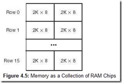
Main memory is usually larger than one RAM chip. Consequently, these chips are combined into a single memory module to give the desired memory size. For example, suppose you need to build a 32K x 16 memory and all you have are 2K x 8 RAM chips. You could connect 16 rows and 2 columns of chips together as shown in Figure 4.5.
Each row of chips addresses 2K words (assuming the machine is word-addressable), but it requires two chips to handle the full width. Addresses for this memory must have 15 bits (there are 32K = 25 x 210 words to access). But each chip pair (each row) requires only 11 address lines (each chip pair holds only 211 words). In this situation, a decoder would be needed to decode the leftmost 4 bits of the address to determine which chip pair holds the desired address. Once the proper chip pair has been located, the remaining 11 bits would be input into another decoder to find the exact address within the chip pair.
A single shared memory module causes sequentialization of access. Memory interleaving, which splits memory across multiple memory modules (or banks), can be used to help relieve this. With low-order interleaving, the low-order bits of the address are used to select the bank; in high-order interleaving, the high-order bits of the address are used.
High-order interleaving, the more intuitive organization, distributes the addresses so that each module contains consecutive addresses, as we see with the 32 addresses in Figure 4.6.
Low-order interleaved memory places consecutive words of memory in different memory modules. Figure 4.7 shows low-order interleaving on 32 addresses.
With the appropriate buses using low-order interleaving, a read or write using one module can be started before a read or write using another module actually completes (reads and writes can be overlapped).
The memory concepts we have covered are very important and appear in various places in the remaining chapters, in particular in Chapter 6, which discusses memory in detail. The key concepts to focus on are: (1) Memory addresses are unsigned binary values (although we often view them as hex values because it is easier), and (2) The number of items to be addressed determines the numbers of bits that occur in the address. Although we could always use more bits for the address than required, that is seldom done because minimization is an important concept in computer design.
4.1.6 Interrupts
We have introduced the basic hardware information required for a solid understanding of computer architecture: the CPU, buses, the control unit, registers, clocks, I/O, and memory. However, there is one more concept we need to cover that deals with how these components interact with the processor: Interrupts are events that alter (or interrupt) the normal flow of execution in the system. An interrupt can be triggered for a variety of reasons, including:
-
I/O requests
-
Arithmetic errors (e.g., division by zero)
-
Arithmetic underflow or overflow
-
Hardware malfunction (e.g., memory parity error)
-
User-defined break points (such as when debugging a program)
-
Page faults (this is covered in detail in Chapter 6)
-
Invalid instructions (usually resulting from pointer issues)
-
Miscellaneous
The actions performed for each of these types of interrupts (called interrupt handling) are very different. Telling the CPU that an I/O request has finished is much different from terminating a program because of division by zero. But these actions are both handled by interrupts because they require a change in the normal flow of the program’s execution.
An interrupt can be initiated by the user or the system, can be maskable (disabled or ignored) or nonmaskable (a high priority interrupt that cannot be disabled and must be acknowledged), can occur within or between instructions, may be synchronous (occurs at the same place every time a program is executed) or asynchronous (occurs unexpectedly), and can result in the program terminating or continuing execution once the interrupt is handled. Interrupts are covered in more detail in Section 4.3.2 and in Chapter 7.
Now that we have given a general overview of the components necessary for a computer system to function, we proceed by introducing a simple, yet functional, architecture to illustrate these concepts.
4.2 Marie
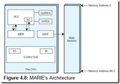
MARIE, a Machine Architecture that is Really Intuitive and Easy, is a simple architecture consisting of memory (to store programs and data) and a CPU (consisting of an ALU and several registers). It has all the functional components necessary to be a real working computer. MARIE will help illustrate the concepts in this and the preceding three chapters. We describe MARIE’s architecture in the following sections.
4.2.1 The Architecture
MARIE has the following characteristics:
-
Binary, two’s complement
-
Stored program, fixed word length
-
Word (but not byte) addressable
-
4K words of main memory (this implies 12 bits per address)
-
16-bit instructions, 4 for the opcode and 12 for the address
-
A 16-bit accumulator (AC)
-
A 16-bit instruction register (IR)
-
A 16-bit memory buffer register (MBR)
-
A 12-bit program counter (PC)
-
A 12-bit memory address register (MAR)
-
An 8-bit input register
-
An 8-bit output register
Figure 4.8 shows the architecture for MARIE.
Before we continue, we need to stress one important point about memory. In Chapter 8, we presented a simple memory built using D flip-flops. We emphasize again that each location in memory has a unique address (represented in binary) and each location can hold a value. These notions of the address versus what is actually stored at that address tend to be confusing. To help avoid confusion, just visualize a post office. There are post office boxes with various “addresses” or numbers. Inside the post office box, there is mail. To get the mail, the number of the post office box must be known. The same is true for data or instructions that need to be fetched from memory. The contents of any memory address are manipulated by specifying the address of that memory location. We shall see that there are many different ways to specify this address.
4.2.2 Registers and Buses
Registers are storage locations within the CPU (as illustrated in Figure 4.8). The ALU (arithmetic logic unit) portion of the CPU performs all of the processing (arithmetic operations, logic decisions, and so on). The registers are used for very specific purposes when programs are executing: They hold values for temporary storage, data that is being manipulated in some way, or results of simple calculations. Many times, registers are referenced implicitly in an instruction, as we see when we describe the instruction set for MARIE that follows in Section 4.2.3.
In MARIE, there are seven registers, as follows:
-
AC: The accumulator, which holds data values. This is a general purpose register and holds data that the CPU needs to process. Most computers today have multiple general purpose registers.
-
MAR: The memory address register, which holds the memory address of the data being referenced.
-
MBR: The memory buffer register, which holds either the data just read from memory or the data ready to be written to memory.
-
PC: The program counter, which holds the address of the next instruction to be executed in the program.
-
IR: The instruction register, which holds the next instruction to be executed.
-
InREG: The input register, which holds data from the input device.
-
OutREG: The output register, which holds data for the output device.
The MAR, MBR, PC, and IR hold very specific information and cannot be used for anything other than their stated purposes. For example, we could not store an arbitrary data value from memory in the PC. We must use the MBR or the AC to store this arbitrary value. In addition, there is a status or flag register that holds information indicating various conditions, such as an overflow in the ALU. However, for clarity, we do not include that register explicitly in any figures.
MARIE is a very simple computer with a limited register set. Modern CPUs have multiple general purpose registers, often called user-visible registers, that perform functions similar to those of the AC. Today’s computers also have additional registers; for example, some computers have registers that shift data values and other registers that, if taken as a set, can be treated as a list of values.
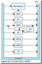
MARIE cannot transfer data or instructions into or out of registers without a bus. In MARIE, we assume a common bus scheme. Each device connected to the bus has a number, and before the device can use the bus, it must be set to that identifying number. We also have some pathways to speed up execution. We have a communication path between the MAR and memory (the MAR provides the inputs to the address lines for memory so the CPU knows where in memory to read or write), and a separate path from the MBR to the AC. There is also a special path from the MBR to the ALU to allow the data in the MBR to be used in arithmetic operations. Information can also flow from the AC through the ALU and back into the AC without being put on the common bus. The advantage gained using these additional pathways is that information can be put on the common bus in the same clock cycle in which data is put on these other pathways, allowing these events to take place in parallel. Figure 4.9 shows the data path (the path that information follows) in MARIE.
4.2.3 The Instruction Set Architecture
MARIE has a very simple, yet powerful, instruction set. The instruction set architecture (ISA) of a machine specifies the instructions that the computer can perform and the format for each instruction. The ISA is essentially an interface between the software and the hardware. Some ISAs include hundreds of instructions. We mentioned previously that each instruction for MARIE consists of 16 bits. The most significant 4 bits, bits 12-15, make up the opcode that specifies the instruction to be executed (which allows for a total of 16 instructions). The least significant 12 bits, bits 0-11, form an address, which allows for a maximum memory size of 212 – 1. The instruction format for MARIE is shown in Figure 4.10.
Most ISAs consist of instructions for processing data, moving data, and controlling the execution sequence of the program. MARIE’s instruction set consists of the instructions shown in Table 4.2.
Table 4.2: MARIE’s Instruction Set
The Load instruction allows us to move data from memory into the CPU (via the MBR and the AC). All data (which includes anything that is not an instruction) from memory must move first into the MBR and then into either the AC or the ALU; there are no other options in this architecture. Notice that the Load instruction does not have to name the AC as the final destination; this register is implicit in the instruction. Other instructions reference the AC register in a similar fashion. The Store instruction allows us to move data from the CPU back to memory. The Add and Subt instructions add and subtract, respectively, the data value found at address X to or from the value in the AC. The data located at address X is copied into the MBR where it is held until the arithmetic operation is executed. Input and Output allow MARIE to communicate with the outside world.
Input and output are complicated operations. In modern computers, input and output are done using ASCII bytes. This means that if you type in the number 32 on the keyboard as input, it is actually read in as the ASCII character “3” followed by “2.” These two characters must be converted to the numeric value 32 before they are stored in the AC. Because we are focusing on how a computer works, we are going to assume that a value input from the keyboard is “automatically” converted correctly. We are glossing over a very important concept: How does the computer know whether an input/output value is to be treated as numeric or ASCII, if everything that is input or output is actually ASCII? The answer is that the computer knows through the context of how the value is used. In MARIE, we assume numeric input and output only. We also allow values to be input as decimal and assume there is a “magic conversion” to the actual binary values that are stored. In reality, these are issues that must be addressed if a computer is to work properly.
The Halt command causes the current program execution to terminate. The Skipcond instruction allows us to perform conditional branching (as is done with “while” loops or “if” statements). When the Skipcond instruction is executed, the value stored in the AC must be inspected. Two of the address bits (let’s assume we always use the two address bits closest to the opcode field, bits 10 and 11) specify the condition to be tested. If the two address bits are 00, this translates to “skip if the AC is negative.” If the two address bits are 01 (bit eleven is 0 and bit ten is 1), this translates to “skip if the AC is equal to 0.” Finally, if the two address bits are 10 (or 2), this translates to “skip if the AC is greater than 0.” By “skip” we simply mean jump over the next instruction. This is accomplished by incrementing the PC by 1, essentially ignoring the following instruction, which is never fetched. The Jump instruction, an unconditional branch, also affects the PC. This instruction causes the contents of the PC to be replaced with the value of X, which is the address of the next instruction to fetch.
We wish to keep the architecture and the instruction set as simple as possible and yet convey the information necessary to understand how a computer works. Therefore, we have omitted several useful instructions. However, you will see shortly that this instruction set is still quite powerful. Once you gain familiarity with how the machine works, we will extend the instruction set to make programming easier.
Let’s examine the instruction format used in MARIE. Suppose we have the following 16-bit instruction:
The leftmost 4 bits indicate the opcode, or the instruction to be executed. 0001 is binary for 1, which represents the Load instruction. The remaining 12 bits indicate the address of the value we are loading, which is address 3 in main memory. This instruction causes the data value found in main memory, address 3, to be copied into the AC. Consider another instruction:
The leftmost four bits, 0011, are equal to 3, which is the Add instruction. The address bits indicate address 00D in hex (or 13 decimal). We go to main memory, get the data value at address 00D, and add this value to the AC. The value in the AC would then change to reflect this sum. One more example follows:
The opcode for this instruction represents the Skipcond instruction. Bits ten and eleven (read left to right, or bit eleven followed by bit ten) are 10, indicating a value of 2. This implies a “skip if AC greater than or equal to 0.” If the value in the AC is less than zero, this instruction is ignored and we simply go on to the next instruction. If the value in the AC is greater than or equal to zero, this instruction causes the PC to be incremented by 1, thus causing the instruction immediately following this instruction in the program to be ignored (keep this in mind as you read the following section on the instruction cycle).
These examples bring up an interesting point. We will be writing programs using this limited instruction set. Would you rather write a program using the commands Load, Add, and Halt, or their binary equivalents 0001, 0011, and 0111? Most people would rather use the instruction name, or mnemonic, for the instruction, instead of the binary value for the instruction. Our binary instructions are called machine instructions. The corresponding mnemonic instructions are what we refer to as assembly language instructions. There is a one-to-one correspondence between assembly language and machine instructions. When we type in an assembly language program (i.e., using the instructions listed in Table 4.2), we need an assembler to convert it to its binary equivalent. We discuss assemblers in Section 4.5.
4.2.4 Register Transfer Notation
We have seen that digital systems consist of many components, including arithmetic logic units, registers, memory, decoders, and control units. These units are interconnected by buses to allow information to flow through the system. The instruction set presented for MARIE in the preceding sections constitutes a set of machine level instructions used by these components to execute a program. Each instruction appears to be very simplistic; however, if you examine what actually happens at the component level, each instruction involves multiple operations. For example, the Load instruction loads the contents of the given memory location into the AC register. But, if we observe what is happening at the component level, we see that multiple “mini-instructions” are being executed. First, the address from the instruction must be loaded into the MAR. Then the data in memory at this location must be loaded into the MBR. Then the MBR must be loaded into the AC. These mini-instructions are called microoperations and specify the elementary operations that can be performed on data stored in registers.
The symbolic notation used to describe the behavior of microoperations is called register transfer notation (RTN) or register transfer language (RTL). We use the notation M[X] to indicate the actual data stored at location X in memory, and ¬ to indicate a transfer of information. In reality, a transfer from one register to another always involves a transfer onto the bus from the source register, and then a transfer off the bus into the destination register. However, for the sake of clarity, we do not include these bus transfers, assuming that you understand that the bus must be used for data transfer.
We now present the register transfer notation for each of the instructions in the ISA for MARIE.
Load X
Recall that this instruction loads the contents of memory location X into the AC. However, the address X must first be placed into the MAR. Then the data at location M[MAR] (or address X) is moved into the MBR. Finally, this data is placed in the AC.
MAR ¬ X
MBR ¬ M[MAR], AC ¬ MBR
Because the IR must use the bus to copy the value of X into the MAR, before the data at location X can be placed into the MBR, this operation requires two bus cycles. Therefore, these two operations are on separate lines to indicate they cannot occur during the same cycle. However, because we have a special connection between the MBR and the AC, the transfer of the data from the MBR to the AC can occur immediately after the data is put into the MBR, without waiting for the bus.
Store X
This instruction stores the contents of the AC in memory location X:
MAR ¬ X, MBR ¬ AC
M[MAR] ¬ MBR
Add X
The data value stored at address X is added to the AC. This can be accomplished as follows:
MAR ¬ X
MBR ¬ M[MAR]
AC ¬ AC + MBR
Subt X
Similar to Add, this instruction subtracts the value stored at address X from the accumulator and places the result back in the AC:
MAR ¬ X
MBR ¬ M[MAR]
AC ¬ AC - MBR
Input
Any input from the input device is first routed into the InREG. Then the data is transferred into the AC.
AC ¬ InREG
Output
This instruction causes the contents of the AC to be placed into the OutREG, where it is eventually sent to the output device.
OutREG ¬ AC
Halt
No operations are performed on registers; the machine simply ceases execution.
Skipcond
Recall that this instruction uses the bits in positions 10 and 11 in the address field to determine what comparison to perform on the AC. Depending on this bit combination, the AC is checked to see whether it is negative, equal to zero, or greater than zero. If the given condition is true, then the next instruction is skipped. This is performed by incrementing the PC register by 1.
if IR[11-10] = 00 then           {if bits 10 and 11 in the IR are both 0}
    If AC < 0 then PC ¬ PC+1
else If IR[11-10] = 01 then      {if bit 11 = 0 and bit 10 = 1}
    If AC = 0 then PC ¬ PC + 1
else If IR[11-10] = 10 then      {if bit 11 = 1 and bit 10 = 0}
    If AC > 0 then PC ¬ PC + 1
If the bits in positions ten and eleven are both ones, an error condition results. However, an additional condition could also be defined using these bit values.
Jump X
This instruction causes an unconditional branch to the given address, X. Therefore, to execute this instruction, X must be loaded into the PC.
PC ¬ X
In reality, the lower or least significant 12 bits of the instruction register (or IR[11-0]) reflect the value of X. So this transfer is more accurately depicted as:
PC ¬ IR[11-0]
However, we feel that the notation PC ¬ X is easier to understand and relate to the actual instructions, so we use this instead.
Register transfer notation is a symbolic means of expressing what is happening in the system when a given instruction is executing. RTN is sensitive to the data path, in that if multiple microoperations must share the bus, they must be executed in a sequential fashion, one following the other.
4.3 Instruction Processing
Now that we have a basic language with which to communicate ideas to our computer, we need to discuss exactly how a specific program is executed. All computers follow a basic machine cycle: the fetch, decode, and execute cycle.
4.3.1 The Fetch-Decode-Execute Cycle
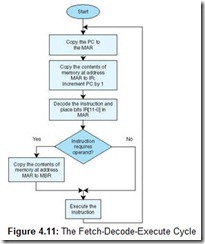
The fetch-decode-execute cycle represents the steps that a computer follows to run a program. The CPU fetches an instruction (transfers it from main memory to the instruction register), decodes it (determines the opcode and fetches any data necessary to carry out the instruction), and executes it (performs the operation(s) indicated by the instruction). Notice that a large part of this cycle is spent copying data from one location to another. When a program is initially loaded, the address of the first instruction must be placed in the PC. The steps in this cycle, which take place in specific clock cycles, are listed below. Note that Steps 1 and 2 make up the fetch phase, Step 3 makes up the decode phase, and Step 4 is the execute phase.
-
Copy the contents of the PC to the MAR: MAR ¬ PC.
-
Go to main memory and fetch the instruction found at the address in the MAR, placing this instruction in the IR; increment PC by 1 (PC now points to the next instruction in the program): IR ¬ M[MAR] and then PC ¬ PC+1. (Note: Because MARIE is word-addressable, the PC is incremented by one, which results in the next word’s address occupying the PC. If MARIE were byte-addressable, the PC would need to be incremented by 2 to point to the address of the next instruction, because each instruction would require two bytes. On a byte-addressable machine with 32-bit words, the PC would need to be incremented by 4.)
-
Copy the rightmost 12 bits of the IR into the MAR; decode the leftmost four bits to determine the opcode, MAR ¬ IR[11–0], and decode IR[15–12].
-
If necessary, use the address in the MAR to go to memory to get data, placing the data in the MBR (and possibly the AC), and then execute the instruction MBR ¬ M[MAR] and execute the actual instruction.
This cycle is illustrated in the flowchart in Figure 4.11.
Note that computers today, even with large instruction sets, long instructions, and huge memories, can execute millions of these fetch-decode-execute cycles in the blink of an eye.
4.3.2 Interrupts and I/O
Chapter 7 is dedicated to input and output. However, we will discuss some basic concepts of I/O at this point, to make sure you understand the entire process of how a program executes.
MARIE has two registers to accommodate input and output. The input register holds data being transferred from an input device into the computer; the output register holds information ready to be sent to an output device. The timing used by these two registers is very important. For example, if you are entering input from the keyboard and type very fast, the computer must be able to read each character that is put into the input register. If another character is entered into that register before the computer has a chance to process the current character, the current character is lost. It is more likely, since the processor is very fast and keyboard input is very slow, that the processor might read the same character from the input register multiple times. We must avoid both of these situations.
MARIE addresses these problems by using interrupt-driven I/O. (A detailed discussion of the various types of I/O can be found in Chapter 7.) When the CPU executes an input or output instruction, the appropriate I/O device is notified. The CPU then continues with other useful work until the device is ready. At that time, the device sends an interrupt signal to the CPU. The CPU then processes the interrupt, after which it continues with the normal fetch-decode-execute cycle. This process requires the following:
-
A signal (interrupt) from the I/O device to the CPU indicating that input or output is complete
-
Some means of allowing the CPU to detour from the usual fetch-decode-execute cycle to “recognize” this interrupt
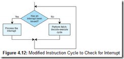
The method most computers use to process an interrupt is to check to see if an interrupt is pending at the beginning of each fetch-decode-execute cycle. If so, the interrupt is processed, after which the machine execution cycle continues. If no interrupt is present, processing continues as normal. The path of execution is illustrated in the flowchart in Figure 4.12.
Typically, the input or output device sends an interrupt by using a special register, the status or flag register. A special bit is set to indicate an interrupt has occurred. For example, as soon as input is entered from the keyboard, this bit is set. The CPU checks this bit at the beginning of every machine cycle. When it is set, the CPU processes an interrupt. When it is not set, the CPU performs a normal fetch-decode-execute cycle, processing instructions in the program it is currently executing.
When the CPU finds the interrupt bit set it executes an interrupt routine that is determined by the type of interrupt that has occurred. Input/output interrupts are not the only types of interrupts that can occur when a program is executing. Have you ever typed a Ctrl-break or Ctrl-C to stop a program? This is another example of an interrupt. There are external interrupts generated by an external event (such as input/output or power failure), internal interrupts generated by some exception condition in the program (such as division by zero, stack overflow, or protection violations) and software interrupts generated by executing an instruction in the program (such as one that requires a program to switch from running at one level, such as user level, to another level, such as kernel level).
Regardless of which type of interrupt has been invoked, the interrupt handling process is the same. After the CPU recognizes an interrupt request, the address of the interrupt service routine is determined (usually by hardware) and the routine (very much like a procedure) is executed. The CPU switches from running the program to running a specialized procedure to deal with the interrupt. The normal fetch-decode-execute cycle is run on the instructions in the interrupt service routine until that code has been run to completion. The CPU then switches back to the program it was running before the interrupt occurred. The CPU must return to the exact point at which it was running in the original program. Therefore, when the CPU switches to the interrupt service routine, it must save the contents of the PC, the contents of all other registers in the CPU, and any status conditions that exist for the original program. When the interrupt service routine is finished, the CPU restores the exact same environment in which the original program was running, and then begins fetching, decoding, and executing instructions for the original program.
4.4 A Simple Program
We now present a simple program written for MARIE. In Section 4.6, we present several additional examples to illustrate the power of this minimal architecture. It can even be used to run programs with procedures, various looping constructs, and different selection options.
Our first program adds two numbers together (both of which are found in main memory), storing the sum in memory. (We forgo input/output for now.)
Table 4.3 lists an assembly language program to do this, along with its corresponding machine-language program. The list of instructions under the Instruction column constitutes the actual assembly language program. We know that the fetch-decode-execute cycle starts by fetching the first instruction of the program, which it finds by loading the PC with the address of the first instruction when the program is loaded for execution. For simplicity, let’s assume our programs in MARIE are always loaded starting at address 100 (in hex).
Table 4.3: A Program to Add Two Numbers
The list of instructions under the Binary Contents of Memory Address column constitutes the actual machine language program. It is often easier for humans to read hexadecimal as opposed to binary, so the actual contents of memory are displayed in hexadecimal.
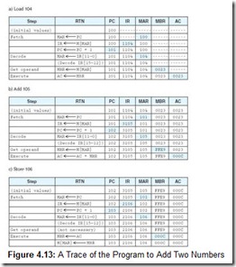
This program loads 002316 (or decimal value 35) into the AC. It then adds the hex value FFE9 (decimal -23) that it finds at address 105. This results in a value of 12 in the AC. The Store instruction stores this value at memory location 106. When the program is done, the binary contents of location 106 change to 0000000000001100, which is hex 000C, or decimal 12. Figure 4.13 indicates the contents of the registers as the program executes.
The last RTN instruction in Part c places the sum at the proper memory location. The statement “decode IR[15-12]” simply means the instruction must be decoded to determine what is to be done. This decoding can be done in software (using a microprogram) or in hardware (using hardwired circuits). These two concepts are covered in more detail in Section 4.7.
Note that there is a one-to-one correspondence between the assembly language and the machine language instructions. This makes it easy to convert assembly language into machine code. Using the instruction tables given in this chapter, you should be able to hand assemble any of our example programs. For this reason, we look at only the assembly language code from this point on. Before we present more programming examples, however, a discussion of the assembly process is in order.
4.5 A Discussion on Assemblers
In the program shown in Table 4.3 it is a simple matter to convert from the assembly language instruction Load 104, for example, to the machine language instruction 1104 (in hex). But why bother with this conversion? Why not just write in machine code? Although it is very efficient for computers to see these instructions as binary numbers, it is difficult for human beings to understand and program in sequences of zeros and ones. We prefer words and symbols over long numbers, so it seems a natural solution to devise a program that does this simple conversion for us. This program is called an assembler.
4.5.1 What Do Assemblers Do?
An assembler’s job is to convert assembly language (using mnemonics) into machine language (which consists entirely of binary values, or strings of zeros and ones). Assemblers take a programmer’s assembly language program, which is really a symbolic representation of the binary numbers, and convert it into binary instructions, or the machine code equivalent. The assembler reads a source file (assembly program) and produces an object file (the machine code).
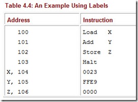
Substituting simple alphanumeric names for the opcodes makes programming much easier. We can also substitute labels (simple names) to identify or name particular memory addresses, making the task of writing assembly programs even simpler. For example, in our program to add two numbers, we can use labels to indicate the memory addresses, thus making it unnecessary to know the exact memory address of the operands for instructions. Table 4.4 illustrates this concept.
Table 4.4: An Example Using Labels
When the address field of an instruction is a label instead of an actual physical address, the assembler still must translate it into a real, physical address in main memory. Most assembly languages allow for labels. Assemblers typically specify formatting rules for their instructions, including those with labels. For example, a label might be limited to three characters and may also be required to occur as the first field in the instruction. MARIE requires labels to be followed by a comma.
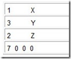
Labels are nice for programmers. However, they make more work for the assembler. It must make two passes through a program to do the translation. This means the assembler reads the program twice, from top to bottom each time. On the first pass, the assembler builds a set of correspondences called a symbol table. For the above example, it builds a table with three symbols: X, Y, and Z. Because an assembler goes through the code from top to bottom, it cannot translate the entire assembly language instruction into machine code in one pass; it does not know where the data portion of the instruction is located if it is given only a label. But after it has built the symbol table, it can make a second pass and “fill in the blanks.”
In the above program, the first pass of the assembler creates the following symbol table:
It also begins to translate the instructions. After the first pass, the translated instructions would be incomplete as follows:
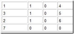
On the second pass, the assembler uses the symbol table to fill in the addresses and create the corresponding machine language instructions. Thus, on the second pass it would know that X is located at address 104, and would then substitute 104 for the X. A similar procedure would replace the Y and Z, resulting in:
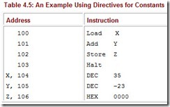
Because most people are uncomfortable reading hexadecimal, most assembly languages allow the data values stored in memory to be specified as binary, hexadecimal, or decimal. Typically, some sort of assembler directive (an instruction specifically for the assembler that is not supposed to be translated into machine code) is given to the assembler to specify which base is to be used to interpret the value. We use DEC for decimal and HEX for hexadecimal in MARIE’s assembly language. For example, we rewrite the program in Table 4.4 as shown in Table 4.5.
Table 4.5: An Example Using Directives for Constants
Instead of requiring the actual binary data value (written in hex), we specify a decimal value by using the directive DEC. The assembler recognizes this directive and converts the value accordingly before storing it in memory. Again, directives are not converted to machine language; they simply instruct the assembler in some way.
Another kind of directive common to virtually every programming language is the comment delimiter. Comment delimiters are special characters that tell the assembler (or compiler) to ignore all text following the special character. MARIE’s comment delimiter is a front slash (“/”), which causes all text between the delimiter and the end of the line to be ignored.
4.5.2 Why Use Assembly Language?
Our main objective in presenting MARIE’s assembly language is to give you an idea of how the language relates to the architecture. Understanding how to program in assembly goes a long way toward understanding the architecture (and vice versa). Not only do you learn basic computer architecture, but you also can learn exactly how the processor works and gain significant insight into the particular architecture on which you are programming. There are many other situations where assembly programming is useful.
Most programmers agree that 10% of the code in a program uses approximately 90% of the CPU time. In time-critical applications, we often need to optimize this 10% of the code. Typically, the compiler handles this optimization for us. The compiler takes a high-level language (such as C++) and converts it into assembly language (which is then converted into machine code). Compilers have been around a long time and in most cases they do a great job. Occasionally, however, programmers must bypass some of the restrictions found in high-level languages and manipulate the assembly code themselves. By doing this, programmers can make the program more efficient in terms of time (and space). This hybrid approach (most of the program written in a high-level language, with part rewritten in assembly) allows the programmer to take advantage of the best of both worlds.
Are there situations in which entire programs should be written in assembly language? If the overall size of the program or response time is critical, assembly language often becomes the language of choice. This is because compilers tend to obscure information about the cost (in time) of various operations and programmers often find it difficult to judge exactly how their compiled programs will perform. Assembly language puts the programmer closer to the architecture, and thus, in firmer control. Assembly language might actually be necessary if the programmer wishes to accomplish certain operations not available in a high-level language.
A perfect example, in terms of both response performance and space-critical design, is found in embedded systems. These are systems in which the computer is integrated into a device that is typically not a computer. Embedded systems must be reactive and often are found in time-constrained environments. These systems are designed to perform either a single instruction or a very specific set of instructions. Chances are you use some type of embedded system every day. Consumer electronics (such as cameras, camcorders, cellular phones, PDAs, and interactive games), consumer products (such as washers, microwave ovens, and washing machines), automobiles (particularly engine control and antilock brakes), medical instruments (such as CAT scanners and heart monitors), and industry (for process controllers and avionics) are just a few of the examples of where we find embedded systems.
The software for an embedded system is critical. An embedded software program must perform within very specific response parameters and is limited in the amount of space it can consume. These are perfect applications for assembly language programming.
4.6 Extending Our Instruction Set
Even though MARIE’s instruction set is sufficient to write any program we wish, there are a few instructions we can add to make programming much simpler. We have 4 bits allocated to the opcode, which implies we can have 16 unique instructions, and we are only using 9 of them. We add the instructions from Table 4.6 to extend our instruction set.
Table 4.6: MARIE’s Extended Instruction Set
The JnS (jump-and-store) instruction allows us to store a pointer to a return instruction and then proceeds to set the PC to a different instruction. This enables us to call procedures and other subroutines, and then return to the calling point in our code once the subroutine has finished. The Clear instruction moves all zeros into the accumulator. This saves the machine cycles that would otherwise be expended in loading a 0 operand from memory.
The AddI instruction (as well as the JumpI instruction) uses a different addressing mode. All previous instructions assume the value in the data portion of the instruction is the direct address of the operand required for the instruction. The AddI instruction uses the indirect addressing mode. (We present more on addressing modes in Chapter 5.) Instead of using the value found at location X as the actual address, we use the value found in X as a pointer to a new memory location that contains the data we wish to use in the instruction. For example, if we have the instruction AddI 400, we would go to location 400, and assuming we found the value 240 stored at location 400, we would go to location 240 to get the actual operand for the instruction. We have, essentially, allowed for pointers in our language.
Returning to our discussion of register transfer notation, our new instructions are represented as follows:
JnS
MBR ¬ PC
MAR ¬ X
M[MAR] ¬ MBR
MBR ¬ X
AC ¬ 1
AC ¬ AC + MBR
PC ¬ AC
Clear
AC ¬ 0
AddI X
MAR ¬ X
MBR ¬ M[MAR]
MAR ¬ MBR
MBR ¬ M[MAR]
AC ¬ AC + MBR
JumpI X
MAR ¬ X
MBR ¬ M[MAR]
PC ¬ MBR
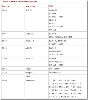
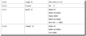
Table 4.7 summarizes MARIE’s entire instruction set.
Table 4.7: MARIE’s Full Instruction Set
Let’s look at some examples using the full instruction set.
![]()
Here is an example using a loop to add five numbers:
Address Instruction Comments
    100 Load         Addr /Load address of first number to be added
    101 Store        Next /Store this address as our Next pointer
    102 Load         Num /Load the number of items to be added
    103 Subt         One /Decrement
    104 Store        Ctr /Store this value in Ctr to control looping
    105 Clear        /Clear AC
Loop, 106 Load       Sum/Load the Sum into AC
    107 AddI         Next /Add the value pointed to by location Next
    108 Store        Sum/Store this Sum
    109 Load         Next /Load Next
    10A Add          One /Increment by one to point to next address
    10B Store        Next /Store in our pointer Next
    10C Load         Ctr /Load the loop control variable
    10D Subt         One /Subtract one from the loop control variable
    10E Store        Ctr /Store this new value in the loop control variable
    10F Skipcond     00 /If control variable < 0, skip next instruction
    110 Jump         Loop /Otherwise, go to Loop
    111 Halt         /Terminate program
Addr, 112 Hex        118 /Numbers to be summed start at location 118
Next, 113 Hex         0 /A pointer to the next number to add
Num, 114 Dec         5 /The number of values to add
Sum, 115 Dec         0 /The sum
Ctr, 116 Hex         0 /The loop control variable
One, 117 Dec         1 /Used to increment and decrement by 1
    118 Dec          10 /The values to be added together
    119 Dec          15
    11A Dec          20
    11B Dec          25
    11C Dec          30
![]()
Although the comments are reasonably explanatory, let’s walk through Example 4.1. Recall that the symbol table stores [label, location] pairs. The Load Addr instruction becomes Load 112, because Addr is located at physical memory address 112. The value of 118 (the value stored at Addr) is then stored in Next. This is the pointer that allows us to “step through” the five values we are adding (located at addresses 118, 119, 11A, 11B, and 11C). The Ctr variable keeps track of how many iterations of the loop we have performed. Since we are checking to see if Ctr is negative to terminate the loop, we start by subtracting one from Ctr. Sum (with an initial value of 0) is then loaded in the AC. The loop begins, using Next as the address of the data we wish to add to the AC. The Skipcond statement terminates the loop when Ctr is negative by skipping the unconditional branch to the top of the loop. The program then terminates when the Halt statement is executed.
Example 4.2 shows how you can use the Skipcond and Jump instructions to perform selection. Although this example illustrates an if/else construct, you can easily modify this to perform an if/then structure, or even a case (or switch) structure.
![]()
This example illustrates the use of an if/else construct to allow for selection. In particular, it implements the following:
if X = Y then
  X := X - 2
else
  Y := Y - X;

Address     Instruction     Comments
If, 100     Load     X      /Load the first value
    101     Subt     Y      /Subtract value of Y and store result in AC
    102     Skipcond 01     /If AC = 0, skip the next instruction
    103     Jump     Else   /Jump to the Else part if AC is not equal to 0
Then, 104   Load     X      /Reload X so it can be doubled
    105     Add      X      /Double X
    106     Store    X      /Store the new value
    107     Jump     Endif  /Skip over Else part to end of If
Else, 108   Load     Y      /Start the Else part by loading Y
    109     Subt     X      /Subtract X from Y
    10A     Store    Y      /Store Y _ X in Y
Endif,      10B      Halt   /Terminate program (it doesn't do much!)
    X,      10C      Dec     12 /Load the loop control variable
    Y,      10D      Dec     20 /Subtract one from the loop control variable
![]()
Example 4.3 demonstrates how JnS and JumpI are used to allow for subroutines. This program includes an END statement, another example of an assembler directive. This statement tells the assembler where the program ends. Other potential directives include statements to let the assembler know where to find the first program instruction, how to set up memory, and whether blocks of code are procedures.
![]()
This example illustrates the use of a simple subroutine to double any number and can be coded:
    100 Load    X     /Load the first number to be doubled
    101 Store   Temp     /Use Temp as a parameter to pass value to Subr
    102 JnS     Subr     /Store return address, jump to procedure
    103 Store   X     /Store first number, doubled
    104 Load    Y     /Load the second number to be doubled
    105 Store   Temp     /Use Temp as a parameter to pass value to Subr
    106 JnS     Subr     /Store return address, jump to procedure
    107 Store    Y     /Store second number, doubled
    108 Halt     /End program
X,  109 Dec     20
Y,  10A Dec     48
Temp, 10B Dec   0
Subr, 10C Hex   0     /Store return address here
    10D Clear     /Clear AC as it was modified by JnS
    10E Load    Temp     /Actual subroutine to double numbers
    10F Add     Temp     /AC now holds double the value of Temp
    110 JumpI   Subr     /Return to calling code
        END
![]()
Using MARIE’s simple instruction set, you should be able to implement any high-level programming language construct, such as loop statements and while statements. These are left as exercises at the end of the chapter.
4.7 A Discussion on Decoding — Hardwired vs. Microprogrammed Control
How does the control unit really function? We have done some hand waving and simply assumed everything works as described, with a basic understanding that, for each instruction, the control unit causes the CPU to execute a sequence of steps correctly. In reality, there must be control signals to assert lines on various digital components to make things happen as described (recall the various digital components from Chapter 3). For example, when we perform an Add instruction in MARIE in assembly language, we assume the addition takes place because the control signals for the ALU are set to “add” and the result is put into the AC. The ALU has various control lines that determine which operation to perform. The question we need to answer is, “How do these control lines actually become asserted?”
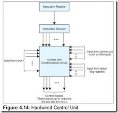
You can take one of two approaches to ensure control lines are set properly. The first approach is to physically connect all of the control lines to the actual machine instructions. The instructions are divided up into fields, and different bits in the instruction are combined through various digital logic components to drive the control lines. This is called hardwired control, and is illustrated in Figure 4.14.
The control unit is implemented using hardware (with simple NAND gates, flip-flops, and counters, for example). We need a special digital circuit that uses, as inputs, the bits from the opcode field in our instructions, bits from the flag (or status) register, signals from the bus, and signals from the clock. It should produce, as outputs, the control signals to drive the various components in the computer. For example, a 4-to-16 decoder could be used to decode the opcode. By using the contents of the IR register and the status of the ALU, this unit controls the registers, the ALU operations, all shifters, and bus access.
The advantage of hardwired control is that it is very fast. The disadvantage is that the instruction set and the control logic are directly tied together by special circuits that are complex and difficult to design or modify. If someone designs a hardwired computer and later decides to extend the instruction set (as we did with MARIE), the physical components in the computer must be changed. This is prohibitively expensive, because not only must new chips be fabricated but also the old ones must e located and replaced.
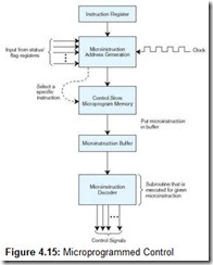
The other approach, called microprogramming, uses software for control, and is illustrated in Figure 4.15.
All machine instructions are input into a special program, the microprogram, to convert the instruction into the appropriate control signals. The microprogram is essentially an interpreter, written in microcode, that is stored in firmware (ROM, PROM, or EPROM), which is often referred to as the control store. This program converts machine instructions of zeros and ones into control signals. Essentially there is one subroutine in this program for each machine instruction. The advantage of this approach is that if the instruction set requires modification, the microprogram is simply updated to match—no change is required in the actual hardware.
Microprogramming is flexible, simple in design, and lends itself to very powerful instruction sets. Microprogramming allows for convenient hardware/software tradeoffs: If what you want is not implemented in hardware (for example, your machine has no multiplication statement), it can be implemented in the microcode. The disadvantage to this approach is that all instructions must go through an additional level of interpretation, slowing down the program execution. In addition to this cost in time, there is a cost associated with the actual development, because appropriate tools are required. We discuss hardwired control versus microprogramming in more detail in Chapter 9.
It is important to note that whether we are using hardwired control or microprogrammed control, timing is critical. The control unit is responsible for the actual timing signals that direct all data transfers and actions. These signals are generated in sequence with a simple binary counter. For example, the timing signals for an architecture might include T1, T2, T3, T4, T5, T6, T7, and T8. These signals control when actions can occur. A fetch for an instruction might occur only when T1 is activated, whereas the fetch for an operand may occur only when T4 is activated. We know that registers can change states only when the clock pulses, but they are also limited to changing in conjunction with a given timing signal. We saw an example of memory in Chapter 3 that included a Write Enable control line. This control line could be ANDed with a timing signal to ensure that memory only changed during specific intervals.
4.8 Real World Examples of Computer Architectures
The MARIE architecture is designed to be as simple as possible so that the essential concepts of computer architecture would be easy to understand without being completely overwhelming. Although MARIE’s architecture and assembly language are powerful enough to solve any problems that could be carried out on a modern architecture using a high-level language such as C++, Ada, or Java, you probably wouldn’t be very happy with the inefficiency of the architecture or with how difficult the program would be to write and to debug! MARIE’s performance could be significantly improved if more storage were incorporated into the CPU by adding more registers. Making things easier for the programmer is a different matter. For example, suppose a MARIE programmer wants to use procedures with parameters. Although MARIE allows for subroutines (programs can branch to various sections of code, execute the code, and then return), MARIE has no mechanism to support the passing of parameters. Programs can be written without parameters, but we know that using them not only makes the program more efficient (particularly in the area of reuse), but also makes the program easier to write and debug.
To allow for parameters, MARIE would need a stack, a data structure that maintains a list of items that can be accessed from only one end. A pile of plates in your kitchen cabinet is analogous to a stack: You put plates on the top and you take plates off the top (normally). For this reason, stacks are often called last-in-first-out structures. (Please see Appendix A at the end of this book for a brief overview of the various data structures.)
We can emulate a stack using certain portions of main memory if we restrict the way data is accessed. For example, if we assume memory locations 0000 through 00FF are used as a stack, and we treat 0000 as the top, then pushing (adding) onto the stack must be done from the top, and popping (removing) from the stack must be done from the top. If we push the value 2 onto the stack, it would be placed at location 0000. If we then push the value 6, it would be placed at location 0001. If we then performed a pop operation, the 6 would be removed. A stack pointer keeps track of the location to which items should be pushed or popped.
MARIE shares many features with modern architectures but is not an accurate depiction of them. In the next two sections, we introduce two contemporary computer architectures to better illustrate the features of modern architectures that, in an attempt to follow Leonardo da Vinci’s advice, were excluded from MARIE. We begin with the Intel architecture (the x86 and the Pentium families) and then follow with the MIPS architecture. We chose these architectures because, although they are similar in some respects, they are built on fundamentally different philosophies. Each member of the x86 family of Intel architectures is known as a CISC (Complex Instruction Set Computer) machine, whereas the Pentium family and the MIPS architectures are examples of RISC (Reduced Instruction Set Computer) machines.
CISC machines have a large number of instructions, of variable length, with complex layouts. Many of these instructions are quite complicated, performing multiple operations when a single instruction is executed (e.g., it is possible to do loops using a single assembly language instruction). The basic problem with CISC machines is that a small subset of complex CISC instructions slows the systems down considerably. Designers decided to return to a less complicated architecture and to hardwire a small (but complete) instruction set that would execute extremely quickly. This meant it would be the compiler’s responsibility to produce efficient code for the ISA. Machines utilizing this philosophy are called RISC machines.
RISC is something of a misnomer. It is true that the number of instructions is reduced. However, the main objective of RISC machines is to simplify instructions so they can execute more quickly. Each instruction performs only one operation, they are all the same size, they have only a few different layouts, and all arithmetic operations must be performed between registers (data in memory cannot be used as operands). Virtually all new instruction sets (for any architectures) since 1982 have been RISC, or some sort of combination of CISC and RISC. We cover CISC and RISC in detail in Chapter 9.
4.8.1 Intel Architectures
The Intel Corporation has produced many different architectures, some of which may be familiar to you. Intel’s first popular chip, the 8086, was introduced in 1979 and used in the IBM PC computer. It handled 16-bit data and worked with 20-bit addresses, thus it could address a million bytes of memory. (A close cousin of the 8086, the 8-bit 8088, was used in many PCs to lower the cost.) The 8086 CPU was split into two parts: the execution unit, which included the general registers and the ALU, and the bus interface unit, which included the instruction queue, the segment registers, and the instruction pointer.
The 8086 had four 16-bit general purpose registers named AX (the primary accumulator), BX (the base register used to extend addressing), CX (the count register), and DX (the data register). Each of these registers was divided into two pieces: the most significant half was designated the “high” half (denoted by AH, BH, CH, and DH), and the least significant was designated the “low” half (denoted by AL, BL, CL, and DL). Various 8086 instructions required the use of a specific register, but the registers could be used for other purposes as well. The 8086 also had three pointer registers: the stack pointer (SP), which was used as an offset into the stack; the base pointer (BP), which was used to reference parameters pushed onto the stack; and the instruction pointer (IP), which held the address of the next instruction (similar to MARIE’s PC). There were also two index registers: the SI (source index) register, used as a source pointer for string operations, and the DI (destination index) register, used as a destination pointer for string operations. The 8086 also had a status flags register. Individual bits in this register indicated various conditions, such as overflow, parity, carry interrupt, and so on.
An 8086 assembly language program was divided into different segments, special blocks or areas to hold specific types of information. There was a code segment (for holding the program), a data segment (for holding the program’s data), and a stack segment (for holding the program’s stack). To access information in any of these segments, it was necessary to specify that item’s offset from the beginning of the corresponding segment. Therefore, segment pointers were necessary to store the addresses of the segments. These registers included the code segment (CS) register, the data segment (DS) register, and the stack segment (SS) register. There was also a fourth segment register, called the extra segment (ES) register, which was used by some string operations to handle memory addressing. Addresses were specified using segment/offset addressing in the form: xxx:yyy, where xxx was the value in the segment register and yyy was the offset.
In 1980, Intel introduced the 8087, which added floating-point instructions to the 8086 machine set as well as an 80-bit wide stack. Many new chips were introduced that used essentially the same ISA as the 8086, including the 80286 in 1982 (which could address 16 million bytes) and the 80386 in 1985 (which could address up to 4 billion bytes of memory). The 80386 was a 32-bit chip, the first in a family of chips often called IA-32 (for Intel Architecture, 32-bit). When Intel moved from the 16-bit 80286 to the 32-bit 80386, designers wanted these architectures to be backward compatible, which means that programs written for a less powerful and older processor should run on the newer, faster processors. For example, programs that ran on the 80286 should also run on the 80386. Therefore, Intel kept the same basic architecture and register sets. (New features were added to each successive model, so forward compatibility was not guaranteed.)
The naming convention used in the 80386 for the registers, which had gone from 16 to 32 bits, was to include an “E” prefix (which stood for “extended”). So instead of AX, BX, CX, and DX, the registers became EAX, EBX, ECX, and EDX. This same convention was used for all other registers. However, the programmer could still access the original registers, AX, AL, and AH, for example, using the original names. Figure 4.16 illustrates how this worked, using the AX register as an example.
The 80386 and 80486 were both 32-bit machines, with 32-bit data buses. The 80486 added a high-speed cache memory (see Chapter 6 for more details on cache and memory), which improved performance significantly.
The Pentium series (Intel changed the name from numbers such as 80486 to “Pentium” because it was unable to trademark the numbers) started with the Pentium processor, which had 32-bit registers and a 64-bit data bus and employed a superscalar design. This means the CPU had multiple ALUs and could issue more than one instruction per clock cycle (i.e., run instructions in parallel). The Pentium Pro added branch prediction, while the Pentium II added MMX technology (which most will agree was not a huge success) to deal with multimedia. The Pentium III added increased support for 3D graphics (using floating point instructions). Historically, Intel used a classic CISC approach throughout its processor series. The more recent Pentium II and III used a combined approach, employing CISC architectures with RISC cores that could translate from CISC to RISC instructions. Intel was conforming to the current trend by moving away from CISC and toward RISC.
The seventh generation family of Intel CPUs introduced the Intel Pentium 4 (P4) processor. This processor differs from its predecessors in several ways, many of which are beyond the scope of this text. Suffice it to say that the Pentium 4 processor has clock rates of 1.4GHz (and higher), uses no less than 42 million transistors for the CPU, and implements something called a “Netburst” microarchitecture. (The processors in the Pentium family, up to this point, had all been based on the same microarchitecture, a term used to describe the architecture below the instruction set.) This new microarchitecture is composed of several innovative technologies, including a hyper-pipeline (we cover pipelines in Chapter 5), a 400MHz (and faster) system bus, and many refinements to cache memory and floating-point operations. This has made the P4 an extremely useful processor for multimedia applications.
The introduction of the Itanium processor in 2001 marked Intel’s first 64-bit chip (IA-64). Itanium includes a register-based programming language and a very rich instruction set. It also employs a hardware emulator to maintain backward compatibility with IA-32/x86 instruction sets. This processor has 4 integer units, 2 floating point units, a significant amount of cache memory at 4 different levels (we study cache levels in Chapter 6), 128 floating point registers, 128 integer registers, and multiple miscellaneous registers for dealing with efficient loading of instructions in branching situations. Itanium can address up to 16GB of main memory.
The assembly language of an architecture reveals significant information about that architecture. To compare MARIE’s architecture to Intel’s architecture, let’s return to Example 4.1, the MARIE program that used a loop to add five numbers. Let’s rewrite the program in x86 assembly language, as seen in Example 4.4. Note the addition of a Data segment directive and a Code segment directive.
![]()
A program using a loop to add five numbers written to run on a Pentium.
    .DATA
Num1    EQU    10    ; Num1 is initialized to 10
    EQU    15    ; Each word following Num1 is initialized
    EQU    20
    EQU    25
    EQU    30
Num    DB    5    ; Initialize the loop counter
Sum    DB    0    ; Initialize the Sum

    .CODE
    LEA    EBX, Num1    ; Load the address of Num1 into EBX
    MOV    ECX, Num    ; Set the loop counter
    MOV    EAX, 0    ; Initialize the sum
    MOV    EDI, 0    ; Initialize the offset (of which number to add)
Start:    ADD    EAX, [EBX+EDI *4]    ; Add the EBXth number to EAX
    INC    EDI    ; Increment the offset by 1
    DEC    ECX    ; Decrement the loop counter by 1
    JG    Start    ; If counter is greater than 0, return to Start
    MOV    Sum, EAX    ; Store the result in Sum
We can make the above program easier to read (which also makes it look less like MARIE’s assembly language) by using the loop statement. Syntactically, the loop instruction resembles a jump instruction, in that it requires a label. The above loop can be rewritten as follows:
    MOV    ECX, Num    ; Set the counter
Start: ADD    EAX, [EBX + EDI + 4]
    INC    EDI
    LOOP Start
    MOV    Sum, EAX
![]()
The loop statement in x86 assembly is similar to the do…while construct in C, C++, or Java. The difference is that there is no explicit loop variable-the ECX register is assumed to hold the loop counter. Upon execution of the loop instruction, the processor decreases ECX by one, and then tests ECX to see if it is equal to zero. If it is not zero, control jumps to Start; if it is zero, the loop terminates. The loop statement is an example of the types of instructions that can be added to make the programmer’s job easier, but which aren’t necessary for getting the job done.
4.8.2 MIPS Architectures
The MIPS family of CPUs has been one of the most successful and flexible designs of its class. The MIPS R3000, R4000, R5000, R8000, and R10000 are some of the many registered trademarks belonging to MIPS Technologies, Inc. MIPS chips are used in embedded systems, in addition to computers (such as Silicon Graphics machines) and various computerized toys (Nintendo and Sony use the MIPS CPU in many of their products). Cisco, a very successful manufacturer of Internet routers, uses MIPS CPUs as well.
The first MIPS ISA was MIPS I, followed by MIPS II through MIPS V. The current ISAs are referred to as MIPS32 (for the 32-bit architecture) and MIPS64 (for the 64-bit architecture). Our discussion in this section is focused on MIPS32. It is important to note that MIPS Technologies made a decision similar to that of Intel-as the ISA evolved, backward compatibility was maintained. And like Intel, each new version of the ISA included operations and instructions to improve efficiency and handle floating point values. The new MIPS32 and MIPS64 architectures have significant improvements in VLSI technology and CPU organization. The end result is notable cost and performance benefits over traditional architectures.
Like IA-32 and IA-64, the MIPS ISA embodies a rich set of instructions, including arithmetic, logical, comparison, data transfer, branching, jumping, shifting, and multimedia instructions. MIPS is a load/store architecture, which means that all instructions (other than the load and store instructions) must use registers as operands (no memory operands are allowed). MIPS32 has 168 32-bit instructions, but many are similar. For example, there are six different add instructions, all of which add numbers, but they vary in the operands and registers used. This idea of having multiple instructions for the same operation is common in assembly language instruction sets. Another common instruction is the MIPS NOP (no-op) instruction, which does nothing except eat up time (NOPs are used in pipelining as we see in Chapter 5).
The CPU in a MIPS32 architecture has 32 32-bit general purpose registers numbered r0 through r31. (Two of these have special functions: r0 is hard-wired to a value of 0 and r31 is the default register for use with certain instructions, which means it does not have to be specified in the instruction itself.) In MIPS assembly, these 32 general purpose registers are designated $0, $1, . . . , $31. Register 1 is reserved, and registers 26 and 27 are used by the operating system kernel. Registers 28, 29, and 30 are pointer registers. The remaining registers can be referred to by number, using the naming convention shown in Table 4.8. For example, you can refer to register 8 as $8 or as $t0.
Table 4.8: MIPS32 Register Naming Convention
There are two special purpose registers, HI and LO, which hold the results of certain integer operations. Of course, there is a PC (program counter) register as well, giving a total of three special purpose registers.
MIPS32 has 32 32-bit floating point registers that can be used in single-precision floating-point operations (with double-precision values being stored in even-odd pairs of these registers). There are 4 special-purpose floating-point control registers for use by the floating-point unit.
Let’s continue our comparison by writing the programs from Examples 4.1 and 4.4 in MIPS32 assembly language.
![]()
    . . .
        .data
    # $t0 = sum
    # $t1 = loop counter Ctr
Value:    .word 10, 15,20,25,30
    Sum = 0
    Ctr = 5
    .text
    .global main    # declaration of main as a global variable
main:    lw $t0, Sum    # Initialize register containing sum to zero
    lw $t1, Ctr    # Copy Ctr value to register
    la $t2, value    # $t2 is a pointer to current value
while:    blez #t1, end_while    # Done with loop if counter <= 0
    lw #t3, 0($t2)    # Load value offset of 0 from pointer
    add $t0, $t0, $t3    # Add value to sum
    addi $t2, $t2, 4    # Go to next data value
    sub #t1, $t1, 1    # Decrement Ctr
    b while        # Return to top of loop
    la $t4, sum    # Load the address of sum into register
    sw $t0, 0($t4)    # Write the sum into memory location sum
    . . .
![]()
This is similar to the Intel code in that the loop counter is copied into a register, decremented during each interation of the loop, and then checked to see if it is less than or equal to zero. The register names may look formidable, but they are actually easy to work with once you understand the naming conventions.
If you are interested in writing MIPS programs, but don’t have a MIPS machine, there are several simulators that you can use. The most popular is SPIM, a self-contained simulator for running MIPS R2000/R3000 assembly language programs. SPIM provides a simple debugger and implements almost the entire set of MIPS assembly instructions. The SPIM package includes source code and a full set of documentation. It is available for many flavors of Unix (including Linux), Windows (PC), and Windows (DOS), as well as Macintosh. For further information, see the references at the end of this chapter.
If you examine Examples 4.1, 4.4, and 4.5, you will see that the instructions are quite similar. Registers are referenced in different ways and have different names, but the underlying operations are basically the same. Some assembly languages have larger instructions sets, allowing the programmer more choices for coding various algorithms. But, as we have seen with MARIE, a large instruction set is not absolutely necessary to get the job done.
Chapter Summary
This chapter has presented a simple architecture, MARIE, as a means to understand the basic fetch-decode-execute cycle and how computers actually operate. This simple architecture was combined with an ISA and an assembly language, with emphasis given to the relationship between these two, allowing us to write programs for MARIE.
The CPU is the principal component in any computer. It consists of a datapath (registers and an ALU connected by a bus) and a control unit responsible for sequencing the operations and data movement and creating the timing signals. All components use these timing signals to work in unison. The input/output subsystem accommodates getting data into the computer and back out to the user.
MARIE is a very simple architecture designed specifically to illustrate the concepts in this chapter without getting bogged down in too many technical details. MARIE has 4K 16-bit words of main memory, uses 16-bit instructions, and has seven registers. There is only one general purpose register, the AC. Instructions for MARIE use 4 bits for the opcode and 12 bits for an address. Register transfer notation was introduced as a symbolic means for examining what each instruction does at the register level.
The fetch-decode-execute cycle consists of the steps a computer follows to run a program. An instruction is fetched and then decoded, any required operands are then fetched, and finally the instruction is executed. Interrupts are processed at the beginning of this cycle, returning to normal fetch-decode-execute status when the interrupt handler is finished.
A machine language is a list of binary numbers representing executable machine instructions, whereas an assembly language program uses symbolic instructions to represent the numerical data from which the machine language program is derived. Assembly language is a programming language, but does not offer a large variety of data types or instructions for the programmer. Assembly language programs represent a lower-level method of programming.
You would probably agree that programming in MARIE’s assembly language is, at the very least, quite tedious. We saw that most branching must be explicitly performed by the programmer, using jump and branch statements. It is also a large step from this assembly language to a high-level language such as C++ or Ada. However, the assembler is one step in the process of converting source code into something the machine can understand. We have not introduced assembly language with the expectation that you will rush out and become an assembly language programmer. Rather, this introduction should serve to give you a better understanding of machine architecture and how instructions and architectures are related. Assembly language should also give you a basic idea of what is going on behind the scenes in high-level C++, Java, or Ada programs. Although assembly language programs are easier to write for x86 and MIPS than for MARIE, all are more difficult to write and debug than high-level language programs.
Intel and MIPS assembly languages and architectures were introduced (but by no means covered in detail) for two reasons. First, it is interesting to compare the various architectures, starting with a very simple architecture and continuing with much more complex and involved architectures. You should focus on the differences as well as the similarities. Second, although the Intel and MIPS assembly languages looked different from MARIE’s assembly language, they are actually quite comparable. Instructions access memory and registers, and there are instructions for moving data, performing arithmetic and logic operations, and branching. MARIE’s instruction set is very simple and lacks many of the “programmer friendly” instructions that are present in both Intel and MIPS instruction sets. Intel and MIPS also have more registers than MARIE. Aside from the number of instructions and the number of registers, the languages function almost identically.
Review of Essential Terms and Concepts
-
What is the function of a CPU?
-
What purpose does a datapath serve?
-
What does the control unit do?
-
Where are registers located and what are the different types?
-
How does the ALU know which function to perform?
-
Why is a bus often a communications bottleneck?
-
What is the difference between a point-to-point bus and a multipoint bus?
-
Why is a bus protocol important?
-
Explain the differences between data buses, address buses, and control buses.
-
What is a bus cycle?
-
Name three different types of buses and where you would find them.
-
What is the difference between synchronous buses and nonsynchronous buses?
-
What are the four types of bus arbitration?
-
Explain the difference between clock cycles and clock frequency.
-
How do system clocks and bus clocks differ?
-
What is the function of an I/O interface?
-
Explain the difference between memory-mapped I/O and instruction-based I/O.
-
What is the difference between a byte and a word? What distinguishes each?
-
Explain the difference between byte-addressable and word-addressable.
-
Why is address alignment important?
-
List and explain the two types of memory interleaving and the differences between them.
-
Describe how an interrupt works and name four different types.
-
How does a maskable interrupt differ from a nonmaskable interrupt?
-
Why is it that if MARIE has 4K words of main memory, addresses must have 12 bits?
-
Explain the functions of all of MARIE’s registers.
-
What is an opcode?
-
Explain how each instruction in MARIE works.
-
How does a machine language differ from an assembly language? Is the conversion one-to-one (one assembly instruction equals one machine instruction)?
-
What is the significance of RTN?
-
Is a microoperation the same thing as a machine instruction?
-
How does a microoperation differ from a regular assembly language instruction?
-
Explain the steps of the fetch-decode-execute cycle.
-
How does interrupt-driven I/O work?
-
Explain how an assembler works, including how it generates the symbol table, what it does with source and object code, and how it handles labels.
-
What is an embedded system? How does it differ from a regular computer?
-
Provide a trace (similar to the one in Figure 4.13) for Example 4.1.
-
Explain the difference between hardwired control and microprogrammed control.
-
What is a stack? Why is it important for programming?
-
Compare CISC machines to RISC machines.
-
How does Intel’s architecture differ from MIPS?
-
Name four Intel processors and four MIPS processors.
Exercises
-
What are the main functions of the CPU?
-
Explain what the CPU should do when an interrupt occurs. Include in your answer the method the CPU uses to detect an interrupt, how it is handled, and what happens when the interrupt has been serviced.
-
Hints and Answers How many bits would you need to address a 2M x 32 memory if
-
Hints and Answers The memory is byte-addressable?
-
Hints and Answers The memory is word-addressable?
-
-
How many bits are required to address a 4M x 16 main memory if
-
Main memory is byte-addressable?
-
Main memory is word-addressable?
-
-
How many bits are required to address a 1M x 8 main memory if
-
Hints and Answers Suppose that a 2M x 16 main memory is built using 256KB x 8 RAM chips and memory is word-addressable.
-
Hints and Answers How many RAM chips are necessary?
-
Hints and Answers How many RAM chips are there per memory word?
-
Hints and Answers How many address bits are needed for each RAM chip?
-
Hints and Answers How many banks will this memory have?
-
Hints and Answers How many address bits are needed for all of memory?
-
Hints and Answers If high-order interleaving is used, where would address 14 (which is E in hex) be located?
-
Hints and Answers Repeat Exercise 6f for low-order interleaving.
-
-
Redo Exercise 6 assuming a 16M x 16 memory built using 512K x 8 RAM chips.
-
A digital computer has a memory unit with 24 bits per word. The instruction set consists of 150 different operations. All instructions have an operation code part (opcode) and an address part (allowing for only one address). Each instruction is stored in one word of memory.
-
How many bits are needed for the opcode?
-
How many bits are left for the address part of the instruction?
-
What is the maximum allowable size for memory?
-
What is the largest unsigned binary number that can be accommodated in one word of memory?
-
-
Assume a 220 byte memory:
-
Hints and Answers What are the lowest and highest addresses if memory is byte-addressable?
-
Hints and Answers What are the lowest and highest addresses if memory is word-addressable, assuming a 16-bit word?
-
What are the lowest and highest addresses if memory is word-addressable, assuming a 32-bit word?
-
-
Given a memory of 2048 bytes consisting of several 64 Byte x 8 RAM chips, and assuming byte-addressable memory, which of the following seven diagrams indicates the correct way to use the address bits? Explain your answer
-
Explain the steps in the fetch-decode-execute cycle. Your explanation should include what is happening in the various registers.
-
Hints and Answers Explain why, in MARIE, the MAR is only 12 bits wide while the AC is 16 bits wide.
-
List the hexadecimal code for the following program (hand assemble it).
Label Hex Address Instruction 100 Load A 101 Add One 102 Jump S1 S2, 103 Add One 104 Store A 105 Halt S1, 106 Add A 107 Jump S2 A, 108 HEX 0023 One, 109 HEX 0001 -
Hints and Answers What are the contents of the symbol table for the preceding program?
-
Given the instruction set for MARIE in this chapter:
-
Decipher the following MARIE machine language instructions (write the assembly language equivalent):
-
Hints and Answers 0010000000000111
-
1001000000001011
-
0011000000001001
-
-
Write the following code segment in MARIE’s assembly language:
if X > 1 then
   Y := X + X;
   X := 0;
endif;
   Y := Y + 1;
-
What are the potential problems (perhaps more than one) with the following assembly language code fragment (implementing a subroutine) written to run on MARIE? The subroutine assumes the parameter to be passed is in the AC and should double this value. The Main part of the program includes a sample call to the subroutine. You can assume this fragment is part of a larger program.
Main,    Load    X
    Jump    Sub1
Sret,        Store X
    . . .
Sub1,    Add    X
    Jump    Sret
-
-
Write a MARIE program to evaluate the expression A x B + C x D.
-
Write the following code segment in MARIE assembly language:
X := 1;
while X < 10 do
   X := X + 1;
endwhile;
-
Write the following code segment in MARIE assembly language:
Sum := 0;
for X := 1 to 10 do
   Sum := Sum + X;
endwhile;
-
Write a MARIE program using a loop that multiplies two positive numbers by using repeated addition. For example, to multiple 3 x 6, the program would add 3 six times, or 3 + 3 + 3 + 3 + 3 + 3.
-
Write a MARIE subroutine to subtract two numbers.
-
More registers appear to be a good thing, in terms of reducing the total number of memory accesses a program might require. Give an arithmetic example to support this statement. First, determine the number of memory accesses necessary using MARIE and the two registers for holding memory data values (AC and MBR). Then perform the same arithmetic computation for a processor that has more than three registers to hold memory data values.
-
MARIE saves the return address for a subroutine in memory, at a location designated by the jump-and-store instruction. In some architectures, this address is stored in a register, and in many it is stored on a stack. Which of these methods would best handle recursion? Explain your answer.
-
Provide a trace (similar to the one in Figure 4.13) for Example 4.2.
-
Provide a trace (similar to the one in Figure 4.13) for Example 4.3.
-
Suppose we add the following instruction to MARIE’s ISA:
IncSZ Operand
This instruction increments the value with effective address “Operand,” and if this newly incremented value is equal to 0, the program counter is incremented by 1. Basically, we are incrementing the operand, and if this new value is equal to 0, we skip the next instruction. Show how this instruction would be written using RTN.
-
Would you recommend a synchronous bus or an asynchronous bus for use between the CPU and the memory? Explain your answer.
-
* Pick an architecture (other than those covered in this chapter). Do research to find out how your architecture deals with the concepts introduced in this chapter, as was done for Intel and MIPS.
TRUE or FALSE
-
_____ If a computer uses hardwired control, the microprogram determines the instruction set for the machine. This instruction set can never be changed unless the architecture is redesigned.
-
_____ A branch instruction changes the flow of information by changing the PC.
-
_____ Registers are storage locations within the CPU itself.
-
_____ A two-pass assembler generally creates a symbol table during the first pass and finishes the complete translation from assembly language to machine instructions on the second.
-
_____ The MAR, MBR, PC, and IR registers in MARIE can be used to hold arbitrary data values.
-
_____ MARIE has a common bus scheme, which means a number of entities share the bus.
-
_____ An assembler is a program that accepts a symbolic language program and produces the binary machine language equivalent, resulting in a one-to-one correspondence between the assembly language source program and the machine language object program.
-
_____ If a computer uses microprogrammed control, the microprogram determines the instruction set for the machine.
