MULTICORE MICROPROCESSOR UNITS
Multicore processors represent a major evolution in computing technology that beyan at the beyinning of the 21st century. It came at a time when businesses and industries re beginning to exploit the exponential growth of digital data and the globalization of the Internet. Multicore processors will eventually become the pervasive model in computing, business, communication, control and auto- mation, and entertainment due to theiy performance and productivity benefits beyond the capabilities of single-core processors.
5.2.1 Introduction and basics
A multicore processor (also called a chip-level or on-chip multiprocessor) can be defined as a processor with more than one physical core on a single chip (or “die”). Each core contains its own dedicated processing resources similar to an individual CPU, except for the processor side bus, which may be shared between cores. Each core implements optimizations such as superscalar execution, pipelining, and multithreading independently. A system with n cores is most effective when it is presented with n or more threads concurrently. For example, a dual-core processor contains two cores, and a quad-core processor contains four cores. Therefore, for our purposes, a traditional micropro- cessor can be called a single-core processor.
(1) From single core to multicore
From the introduction of Intel’s 8086 through to the Pentium 4, an increase in performance, has been seen with each increase in processor frequency. For example, the Pentium 4 ranged in speed (frequency) from 1.3 to 3.8 GHz over its 8-year lifetime. The physical size of chips has decreased as the number of transistors per chip has increased; clock speeds increased, which boosted the heat buildup across the chip to a dangerous level. Intel’s co-founder, Gordon Moore, is credited with Moore’s law, which has been one of the guiding principles of computer architecture for more than two decades. In 1965, he stated that the number of transistors on a chip will roughly double each year (he later refined this, in 1975, to every two years).
Many techniques are used. performance within a single-core processor chip to Superscalar
processors with the ability to issue multiple instructions concurrently are the standard. In these pipelines, instructions are prefetched, split into subcomponents and executed out-of-order. A major focus of computer architectures is the branch instruction. In order to speed up this process, the processor predicts which path will be taken; if the wrong path is chosen the processor must throw out any data computed while taking the wrong path and backtrack to take the correct path. Often even when an incorrect branch is taken the effect is equivalent to having waited to take the correct path. Branches are also removed by using loop unrolling, and sophisticated neural network-based predictors are used to minimize the misprediction rate. Other techniques used for performance enhancement include register renaming, trace caches, reorder buffers, dynamic software scheduling, and data value prediction
Speeding up processor frequency had run its course in the earlier part of the last decade; computer architects needed a new approach to improve performance. Adding an additional processing core to the same chip would, in theory, result in twice the performance and produce less heat; though in practice the actual speed of each core is slower than the fastest single-core processor. Due to advances in integrated circuit technology, multicore processor technology has become a mainstream element of CPU design, with Intel, AMD, IBM, SUN and Azul etc. all introducing many commercially available multicore chips.
The story for multicore processors started in 2001 and can be summarized as follows:
1. The first dual-core processor in the world, POWER4, was released in 2001 by IBM.
2. AMD promised its first quad-core Opteron processors by midyear in 2005. They would be manufactured using a “native” design that placed four independent cores on a single chip.
3. In late 2006 Intel introduced its first quad-core Xeon processors. The processors were
manufactured by packaging two Intel dual-core processors in a single chip. Intel planned to deliver a dual-core desktop processor based on its 65-nm process technology in 2006.
4. IBM has been offering quad-core Power processors since 2005. Similar to Intel, the chips are
manufactured using a multichip module.
5. SUN introduced the Sparc-based Niagara in late 2005. The chip has eight cores, each operating with four independent threads. By midyear, SUN promises Niagara 2, which will have eight cores, each with eight threads.
6. Azul Systems Inc. introduced its 24-core Vega chip in 2005. In December, the company announced Vega 2, a 48-core processor.
As with any technology, multicore architectures from different manufacturers vary greatly. Intel and AMD are the mainstream manufacturers of microprocessors. Intel produces many different flavors of multicore processors; the Pentium D in desktops, Core 2 Duo is used in both laptop and desktop environments, and the Xeon processor is used in servers. AMD has the Althon lineup for desktops, Turion for laptops, and Opteron for servers/workstations. Although the Core 2 Duo and Athlon 64 X2 run on the same platforms, their architectures differ greatly.
Along with differences in communication and memory configuration, another difference is due to many cores the microprocessor has, and the functions of the different cores. Intel’s current 7300 chipset-based platform combined with the Quad-Core Xeon 7300 processor is the industry’s virtualization platform of choice for microprocessor servers from the second half of 2008. Intel’s traditional rival, AMD, is portrayed by the media as the company with the winning strategy, and 64-bit computing and multicore technology are touted as two areas where AMD has a competitive edge over Intel. Intel has recently bridged the gap with AMD in 64-bit computing with its latest impressive offerings in multicore technology.
In contrast to commercially available two- and four-core machines in 2008, some experts believe that “by 2017 embedded processors could sport 4,096 cores, server CPUs might have 512 cores and desktop chips could use 128 cores”. This rate of growth is astounding, considering that current desktop chips are only on the cusp of using four cores, and a single-core processor has been used for the past 40 years.
(2) Multicore challenges and open problems
Having multiple cores on a single chip gives rise to some problems and challenges. Power and temperature management are two concerns that can increase exponentially with the addition of multiple cores. Cache coherence is another challenge, since all designs discussed above have distributed L1 and in some cases L2 caches which must be coordinated. And finally, using a multicore processor to its full potential is another issue. If programmers do not write applications that take advantage of multiple cores there is no gain, and in some cases there is a loss of performance. Applications need to be written so that different parts can be run concurrently (without any ties to another part of the application that is being run simultaneously).
(a) Power and temperature
If two cores were placed on a single chip without any modification, the chip would, in theory, consume twice as much power and generate a large amount of heat. In the extreme, if a processor overheats the computer may even combust. To account for this, each design runs multiple cores at a lower frequency to reduce power consumption, and to combat unnecessary power consumption, many designs also incorporate a power control unit that has the authority to shut down unused cores or limit the amount of power used. By powering-off unused cores, and using clock gating, the amount of leakage in the chip is reduced. To lessen the heat generated by multiple cores on a single chip, the chip is designed to minimize the number of hot spots and sothat the heat is spread out across the chip. The processor follows a common trend to build temperature monitoring into the system, with its one linear sensor and ten internal digital sensors.
(b) Cache coherence
Cache coherence is a concern in a multicore environment because of distributed L1 and L2 caches. Since each core has its own cache, the copy of the data in that cache may not always be the most up-to- date version. For example, imagine a dual-core processor where each core brought a block of memory into its private cache, and then one core writes a value to a specific location. When the second core
186 CHAPTER 5 Microprocessors
attempts to read that value from its cache, it will not have the most recent version unless its cache entry is invalidated and a cache miss occurs. This cache miss forces the second core’s cache entry to be updated. If this coherence policy was not in place, the wrong data would be read and invalid results would be produced, possibly crashing the program or the entire computer.
In general there are two schemes for cache coherence; a snooping protocol and a directory-based protocol. The snooping protocol only works with a bus-based system, and uses a number of states to determine whether or not it needs to update cache entries, and whether it has control over writing to the block. The directory-based protocol can be used on an arbitrary network and is, therefore, scalable to many processors or cores. This contrast swith snooping, which is not scalable. In this scheme, a directory is used which holds information about which memory locations are being shared in multiple caches, and which are used exclusively by one core’s cache. The directory knows when a block needs to be updated or invalidated.
Intel’s Core 2 Duo tries to speed up cache coherence by being able to query the second core’s L1 cache and the shared L2 cache simultaneously. Having a shared L2 cache also has the added benefit that a coherence protocol does not need to be set for this level. AMD’s Athlon 64 X2, however, has to monitor cache coherence in both L1 and L2 caches. This is made fasterby using the Hyper Transport connection, but still has more overhead than Intel’s model.
Extra memory will be useless if the amount of time required for memory requests to be processed does not improve as well. Redesigning the interconnection network between cores is acrrently a major focus of chip manufacturers. A faster network means a lower latency in inter-core communication and memory transactions. Intel is developing their Quick path interconnect, which is a 20-bit wide bus running between 4.8 and 6.4 GHz; AMD’s new Hyper Transport 3.0 is a 32-bit wide bus and runs at
5.2 GHz. Using five mesh networks gives the Tile architecture a per core bandwidth of up to 1.28 Tbps
(terabits per second).
Despite these efforts, the question remains; which type of interconnect is best suited for multicore processors? Is a bus-based approach better than an interconnection network? Or is a hybrid like the mesh network a better optica?
(c) Multithreading
The last, and most important, issue is using multithreading or other parallel processing techniques to get the most performance out of the multicore processor. Rebuilding applications to be multithreaded means a complete rework by programmers to take best advantage of multicore systems. Programmers have to write applications with subroutines which can run in different cores, meaning that data dependencies will have to be resolved or accounted for (e.g. latency in communication or using a shared cache). Applications should be balanced. If one core is being used much more than another, the programmer is not taking full advantage of the multicore system. Some companies have designed new products with multicore capabilities; Microsoft and Apple’s newest operating systems can run on up to four cores, for example.
Developing software for multicore processors raises some concerns. How does a programmer ensure that a high-priority task gets priority across the whole processor, not just one core? In theory, even if a thread had the highest priority within the core on which it is running, it might not have a high priority across the system as a whole. Another necessary tool for developers is debugging. However, how do we guarantee that the entire system stops and not just the core on which an application is running?
These issues need to be addressed along with the teaching of good parallel programming practices for developers. Once programmers have a basic grasp on how to multithread and program in parallel, instead of sequentially, ramping up to follow Moore’s law will be easier.
5.2.2 Types and architectures
The multicore processor is a special kind of a multiprocessor in which all processors are resident on the same chip. There are two ways of differentiating multicore processors from multiprocessors. Firstly, a multicore processor is a MIMD (multiple-instruction, multiple-data) multiprocessor. In a multicore, different cores execute different threads (multiple-instructions), operating on different parts of memory (multiple-data). Second, a multicore processor is a shared memory multiprocessor, in which all cores share the same memory.
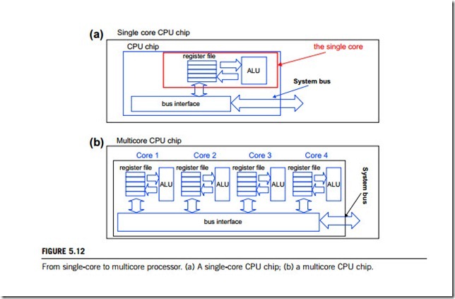
Although the architectures of multicore processors are much more complex than those of single-core processors, there are some common features between them. Figure 5.12 sketches the difference between their architectures. For a single-core processor, one CPU chip just has one core, composed of an ALU (arithmetic logic unit), memory registers and a bus interface with the system bus. However, a multicore chip can have more than one core, although each of these cores also contains ALU, memory registers and bus interface.
(1) Homogeneous and heterogeneous multicore processors
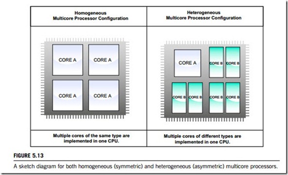
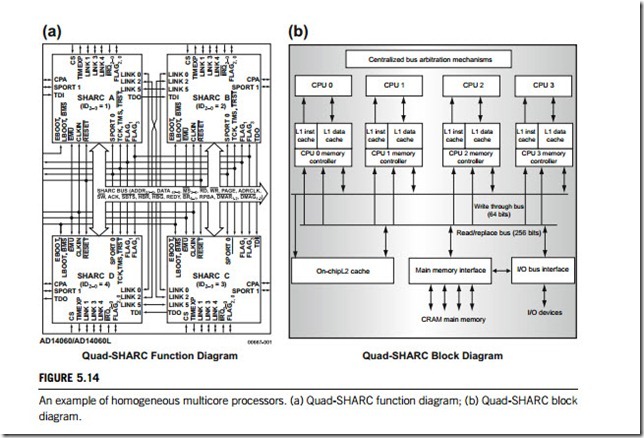
There are two ways of implementing multicore processors. One is homogeneous, or symmetric chip multiprocessing. This involves geometrically increasing the number of cores with each advance in feature size, so either duplicating or quadrupling the same core, and interconnecting them to produce a single, more powerful core as shown in Figure 5.13. We can see such an architecture in the Niagara chip and in the Quad-SHARC DSP, where four similar cores are connected to each other by a crossbar switch, as shown in Figure 5.14.
The other way is heterogeneous or asymmetric chip multiprocessing. This includes a combination of a large core, plus several low-power cores, such as a CPU surrounded by different specialized cores like GPUs (graphical processing units) and others. A heterogeneous, or asymmetric, multicore processor is one does have multiple cores on a single chip, but those cores might be of different designs of both high and low complexity. Figure 5.13 also shows a sample floorplan of an asymmetric chip multiprocessor. It consists of one high-performance core on the left top, and three medium-perfor- mance cores on the right and lower left. Of course, a real heterogeneous multicore can be much more complicated in floorplan. Up to now, heterogeneous multicore processors exist in two typical configurations; Cell multiprocessors and SoC (system on chip), which are discussed in the following paragraphs.
Both approaches will to benefit the industry on the whole. Both are aimed at pursuing a similar goal; increased throughput through parallel hardware, which requires changes to existing software to take advantage of this increased computing power. Many server applications focus primarily on throughput per unit cost and unit power. Desktop users are more interested in single applications or
a few applications at the same time. A multicore processor for desktop users will probably be focused on a smaller number of larger, yet powerful, cores with better single-thread performance.
As the processor becomes more powerful and complex, both its peak and average power increase dramatically. The ability to dynamically switch between different cores and power-down unused cores is the key in asymmetric chip (multicore) multiprocessing. It has been shown that a representative heterogeneous processor using two core types achieves as much as a 63 percent performance improvement over an equivalent-area homogeneous processor. Asymmetric multiprocessors achieve better coverage of a spectrum of load levels.
Using a heterogeneous multicore configuration could significantly reduce processor power dissipation problems. Power consumption and heat dissipation have become key challenges in high- performance processor designs. Recently, the industry has introduced techniques for power reduction, such as clock gating and voltage/frequency scaling, both of which are very effective when applied at the single-core level.
For multiple cores, however, these techniques have limitations. Data must be passed onto different parts of the processor, and may be passed on unused portions that have been gated off, which consumes a substantial amount of power. Gating only reduces dynamic power. Large unused portions of the chip still consume leakage power. This is the same with voltage and frequency scaling techniques.
We believe the best choice core of complex is a heterogeneous multicore processor with both high- and low-complexity cores. Recent research in heterogeneous or asymmetric multicore processors has identified that they have significant advantages over homogeneous multicore processors in terms of power and throughput, and in the performance of parallel applications.
(2) Cell processor
As explained in the previous paragraphs, the “Cell processor” is one of the possible heterogeneous configurations of multicore processors. A Cell processor consists of both control-intensive processor and compute-intensive processor cores, each with its own distinguishing features. This section will discuss its physical architecture.
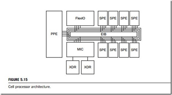
The Cell architecture includes software and hardware cells. A software cell is a program plus its associated data, and a hardware cell is an execution unit with the capability to execute a software cell. There is no fixed architecture (the software cells could float around and can be processed by any available hardware cell), which is very interesting, when combined with the ubiquitous computing idea. Several of these hardware cells can create a bigger Cell computer (Ad Hoc). But this is only an architectural vision; a real-life Cell processor is bound to a single chip, and floating Cells are still only ideas. But the general principle remains the same. A Cell processor consists of a PPE (PowerPC processing element), which acts as the main processor to distribute tasks (software cells). It also has a MFC (memory flow controller), which interfaces between the computing and memory units, and also many SPE (synergistic processing elements), which are hardware cells having their own memory. Nowadays, the Cell CPU is essentially a combination of a power processor with eight small vector processors. All these units are connected via an EIB (element interconnect bus) and communicate with peripheral devices or other CPUs via the FlexIO interface. A single Cell, essentially a network on chip, offers up to 256 Gflop, single precision, floating-point performance. A block diagram of the Cell processor is shown in Figure 5.15.
(a) Prototype
A prototype was produced by using 90 nm silicon on insulator technology, with eight copper layers (wiring). It consists of 241 million transistors at 235 per square mm, and consumes 60 80 W. IBM’s virtualization technology is incorporated in the PPE. The CPU is clocked at 4 GHz at 1.1 V.
(b) The power processing element
The power processing element (PPE) offers the normal PowerPC ISA (instruction set architecture). It is a dual-threaded 64-bit power processor. Its architecture is very simple to guarantee high clock rates, so it uses only in-order execution with a deep super scalar 2-way pipeline with more than 20 stages. It offers a 2×32 kB L1 split cache, a 512 kB L2 cache and virtualization. Altogether the PPE can be seen as a simplified Power processor.
(c) The synergistic processing element (SPE)
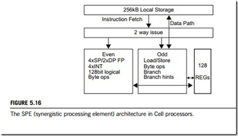
The SPE is essentially a full blown vector CPU with its own RAM (memory). Its ISA has a fixed length of 32 bits. Current SPEs have about 21 million transistors, of which two thirds are dedicated to the SRAM (memory). The processor has no branch prediction or scheduling logic, but relies on the programmer/compiler to find parallelism in the code. It uses two independent pipelines, and issues two instructions per cycle; one SIMD (single-instruction, multiple-data) computation operation and one memory access operation. All instructions are processed strictly in order, and each instruction works with 128-bit compound data items. Four, single-precision, floating-point units and four integer units offer up to 32 GOps each. The single-precision, floating-point, units are not IEEE-754-compliant in terms of rounding and special values, and they can also be used to compute double-precision-floating point numbers which are compliant to the IEEE-754 standard. Their computation is, however, rather slow (3-4 Gflops). The schematic architecture of a single SPE is shown in Figure 5.16. The memory layout of the SPE is also quite special; each SPE has its own 256 kB RAM, which is called local storage (LS). This SRAM storage can be accessed extremely fast in 128-bit lines. Additionally, each SPE has a large register file of 128×128-bit registers which store all available data types. There is no cache, virtual memory support or coherency for the local storage and the data can be moved with DMA
(direct memory access) from/to main memory via the EIB (element interconnect bus). The memory flow controller (MFC) acts like a MMU in this context and provides virtual memory translations for main memory access.
(d) The element interconnect bus
The EIB is the central communication channel inside a Cell processor; it consists of four 128-bit-wide concentric rings. The ring uses buffered, point to point communication to transfer the data and so is scalable. It can move 96 bytes per cycle and is optimized for 1024-bit data blocks. Additional nodes
(e.g. SPEs) can be added easily and increase only the maximal latency of the ring. Each device has a hardware guaranteed bandwidth of 1/numDevices to enhance its suitability for real-time computing.
(e) The I/O interconnect FlexIO
The I/O interconnect connects the Cell processor (the EIB) to the external world (e.g. other Cell processors). It offers 12 unidirectional byte-lanes which are 96 wires. Each lane may transport up to
6.4 GB/s, which makes 76.8 GB accumulated bandwidth. Seven lanes are outgoing (44.8 GB/s) and five lanes incoming (32 GB/s). There are cache coherent (CPU interconnects) and noncoherent links (device interconnects) and two Cell processors can be connected loosely.
(f) The memory interface controller (MIC)
The MIC connects the EIB to the main DRAM memory, which is in this case Rambus XDR memory, which offers a bandwidth of 25.2 GB/s. The memory shows that the Cell will be used for more than game consoles and consumer electronics. The MIC offers virtual memory translation to the PPE and the SPEs. The memory itself is not cached; only the PPE has its own cache hierarchy.
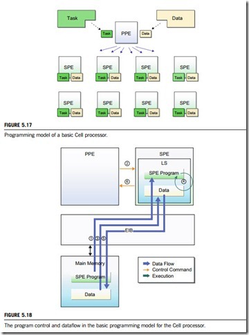
A variety of Cell programming models have been suggested sofar. The most basic among them is shown in Figure 5.17, where the PPE is used for execution of the main program and the SPEs for execution of a sub-program. The main program executed on the PPE (hereinafter called the PPE program) divides a sequence of processes or data, and distributes a segment to every SPE for pro- cessing by the sub-program running on the SPEs (hereinafter called the SPE program). Upon completion of the requested operation, the SPE program returns the processed result to the PPE program.
Let us take a look at how PPE and SPE programs are executed on the Cell architecture, together
with how necessary data are transmitted and received. As explained in Figure 5.18, the dataflow consists of the steps given below:
1. (PPE Program) Loads the SPE program to the LS.
2. (PPE Program) Instructs the SPEs to execute the SPE program.
3. (SPE Program) Transfers required data from the main memory to the LS.
4. (SPE Program) Processes the received data in accordance with the requirements.
5. (SPE Program) Transfers the processed result from the LS to the main memory.
6. (SPE Program) Notifies the PPE program of the termination of processing.
(3) Intel and AMD multicore architectures
Intel and AMD are the mainstream manufacturers of microprocessors. Intel produces many different flavors of multicore processors; the Pentium D is used in desktops, Core 2 Duo is used in both laptop
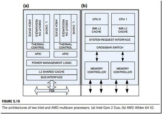
and desktop, and the Xeon processor is used in servers. AMD has the Althon for desktops, Turion for laptops, and Opteron for servers and workstations. Although the Core 2 Duo and Athlon 64 X2 run on the same platforms, their architectures differ greatly. Figure 5.19 shows block diagrams for the Core 2 Duo and Athlon 64 X2. Both architectures are homogeneous dual-core processors. The Core 2 Duo adheres to a shared memory model, with private L1 caches and a shared L2 cache. If a L1 cache miss occurs, both the L2 cache and the second core’s L1 cache are traversed in parallel before sending a request to main memory. By contrast, the Athlon follows a distributed memory model with discrete L2 caches, which share a system request interface, eliminating the need for a bus.
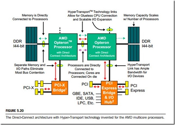
AMD engineers invented Hyper-Transport technology, which presents a high-bandwidth (10 GB/s) low-latency (less than 10 ns) chip-to-chip interconnect mechanism. After inventing this technology, AMD worked to share it with the industry. AMD has also created an enhanced version of Hyper- Transport technology, known as “Coherent Hyper-Transport technology”, that it uses to coordinate the contents of on-chip caches in multiprocessor AMD64 configurations. Figure 5.20 explains these larger configurations, which are best suited for executing computationally intensive applications and for database management. The system request interface also connects the cores with an on-chip memory controller and the Hyper-Transport interconnection. Hyper-Transport effectively reduces the number of buses required in a system, so reducing bottlenecks and increasing bandwidth.
The Larrabee architecture will be Intel’s next step in evolving the visual computing platform. This includes a high-performance, wide SIMD vector processing unit along with a new set of vector in- structions, including integer and floating-point arithmetic, vector memory operations and conditional
instructions. In addition, Larrabee includes a major, new, hardware coherent cache design enabling the many-core architecture. The architecture and instructions have been designed to deliver performance, energy efficiency and general-purpose programmability in order to meet the demands of visual computing and other workloads that are inherently parallel in their nature. Tools are critical to success, and key Intel software products will be enhanced to support the Larrabee architecture and enable unparalleled developer freedom. The industry APIs (application program interfaces), such as DirectX™ and OpenGL, will be supported on Larrabee-based products.
5.2.3 Cores and components
Similar to the single-core processor unit, the multicore processor unit works by relying on the processor and key components including cache, memory and bus. In this subsection, we will discuss these elements of multicore processors.
(1) Core microarchitecture
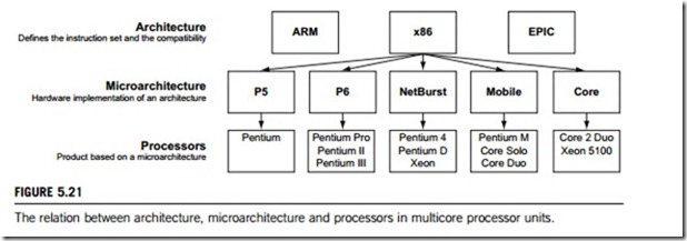
Some features of the new generations of Intel and AMD processors are brand new, but others are not. For example, the underlying architecture named x86 is still the same as the x86 CPU. This architecture defines which kind of instructions the processor can execute, and the way the processor can be accessed, i.e. which software can be used. Both Intel and AMD have been expanding the x86 instruction set continuously, for instance with special MMX (matrix math extension), SSE (streaming SIMD extension) and x86-64 instructions.
As another example, the Bobcat processor, made by AMD, is a very simplified x86 CPU core aiming at low-power x86 processing with values between 1 and 10 W, together with low-voltage operation. According to AMD roadmaps, the Bobcat processor will be incorporated together with GPU (graphic processing unit) cores into processors under the codename “Fusion” (AMD Fusion is the codename for a future microprocessor design, combining general processor execution as well as three- dimensional geometry processing and other functions of modern GPU into a single package.). New multicore processors now incorporate a variety of improvements, particularly in memory prefetching, speculative loads, SIMD execution and branch prediction, yielding an appreciable performance increase.
The defined microarchitecture is the hardware implementation of such architecture. So while AMD and Intel processors are based on the exact same x86 architecture and are therefore 100% compatible, their inner working is completely different due to different microarchitectures. Figure 5.21 explains the relation between architecture, microarchitecture and processors.
One new technology included in the design is Macro-Ops Fusion, which combines two x86 instructions into a single micro-operation. For example, a common code sequence such as a compare followed by a conditional jump would become a single micro-op. Other new technologies include one-cycle throughput (two cycles previously) of all 128-bit SSE instructions and a new power saving design. All components will run at minimum speed, ramping up speed dynamically as needed. This allows the chip to produce less heat, and consume as little power as possible.
(2) Cache memories
In multicore processors, the embedded cache memory architecture must be carefully considered because caches may be dedicated to a particular processor core, or shared among multiple cores. Furthermore, multicore processors typically employ a more complex interconnect mechanism, such as shared bus fabric, to connect the cores, caches, and external memory interfaces often including switches and routers.
In a multicore processor, cache coherency must also be considered. Multicore processors may also require that on-chip memory should be used as a temporary buffer to share data among multiple processors, as well as to store temporary thread context information in a multi-threaded system.
