Zener diodes are closely related to P–N junction diodes. They are constructed to take advantage of reverse current. Zener diodes find wide application for controlling voltage in all types of circuits.
Zener Diode Characteristics
As previously stated, a high reverse-bias voltage applied to a diode may create a high reverse current, which can generate excessive heat and cause a diode to break down. The applied reverse voltage at which the breakdown occurs is called the breakdown voltage (eZ) or peak reverse voltage. A special diode called a zener diode is connected to operate in the reverse-bias mode. It is designed to operate at those voltages that exceed the breakdown voltage. This breakdown region is called the zener region.
When a reverse-bias voltage is applied that is high enough to cause breakdown in a zener diode, a high reverse current (IZ) flows. The reverse current is low until breakdown occurs. After breakdown, the reverse current increases rapidly. This occurs because the resistance of the zener diode decreases as the reverse voltage increases.
The breakdown voltage, or zener voltage (EZ), is determined by the resistivity of the diode. This, in turn, is controlled by the doping technique used during manufacturing. The rated breakdown voltage represents the reverse voltage at the zener test current (iZt). The zener test current is somewhat less than the maximum reverse current the diode can handle. The breakdown voltage is typically rated with 1% to 20% tolerance.
The ability of a zener diode to dissipate power decreases as the temperature increases. Therefore, power dissipation ratings are given for specific temperatures. Power ratings are also based on lead lengths: shorter leads dissipate more power. A derating factor is given by the diode manufacturer to determine the power rating at different tem- peratures from the ones specified in their tables. For example, a derating factor of 6 mW per degree Celsius means that the diode power rating decreases 6 mW for each degree of change in temperature.
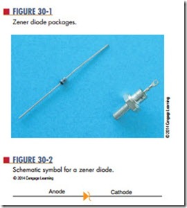
Zener diodes are packaged like P–N junction diodes (Figure 30-1). Low-power zener diodes are mounted in either glass or epoxy. High-power zener diodes are stud mounted with a metal case. The schematic symbol for the zener diode is similar to the P–N junction diode except for the diagonal lines on the cathode bar (Figure 30-2).
Questions
1. What is the unique feature of a zener diode?
2. How is a zener diode connected into a circuit?
3. What determines the voltage at which a zener diode breaks down?
4. What considerations go into determining the power dissipation rating of a zener diode?
Draw and label the schematic symbol used to represent a zener diode.
