Chapter 1: Parallel Interface—The LPT Port
Overview
The parallel interface port was added to computers to allow users to connect a printer. Hence the name: the LPT port. (LPT stands for Line Printer Terminal.) The traditional LPT port, or Standard Parallel Port (SPP) is oriented toward data output; limited data input is also possible. Modifications of the LPT port include the Bidirectional port, the Enhanced Parallel Port (EPP), the Enhanced Capability Port (ECP), and others that expand its functional capabilities, increase productivity, and decrease the processor workload. At first, they were the in-shop solutions of individual manufacturers; later, the IEEE 1284 standard was adopted by the Institute of Electrical and Electronics Engineers.
On the hardware side, the port has an 8-bit data bus, a 5-bit status-monitoring signals bus, and a 4-bit control signals bus. These are brought into a DB-25S connector. TTL levels are used in the LPT port. The low noise tolerance of the TTL interface limits the cable length. There is no galvanic decoupling: The circuit ground of the attached device is connected to the computer’s circuit ground. Because of this, the port is the computer’s vulnerable spot, which can be damaged when the rules for connecting and grounding devices are not followed. The port is usually on the motherboard. Therefore, if it “burns out,” its immediate surroundings often are damaged. The damage may extend to the entire motherboard.
The software side of the LPT port is a collection of registers, located in the input/output (I/O) addressing space. Port registers are addressed relative to the port’s BASE address. The 3BCh, 378h, and 278h addresses are the standard values. The port may use the hardware interrupt line, usually IRQ7 or IRQ5. In enhanced operation modes, the Direct Memory Access (DMA) channel can be used.
The port is supported on the Basic Input/Output System (BIOS) level. It searches for the installed ports during the Power-On Self-Test (POST) routine. Through the Int17h print services (see Section 7.3.3), it provides for the character output (upon polling the readiness status without using hardware interrupts), the initialization of the interface and the printer, and the printer status poll.
More efficient are the services provided by the EPP BIOS, which most modern computers have. It contains advanced service functions to work with multiple devices connected to one port (under the IEEE 1284.3), as well as I/O functions allowing transmission and reception of not only single bytes but also blocks of data. This makes it possible to raise the exchange speed by reducing the overhead associated with calling a BIOS service.
Practically all modern motherboards (starting with Peripheral Component Interconnect (PCI) motherboards for x486 processors) have a built-in LPT port adapter. The LPT port also may be based on Industry Standard Architecture (ISA) expansion cards. On these, the LPT port typically neighbors a couple of communications (COM) ports and disk interface controllers (a Floppy Disk Controller and Integrated Drive Electronics, or FDC+IDE). Usually, there is an LPT port on the Monochrome Display Adapter (MDA) for monochrome text and the Hercules Graphics Card (HGC) for monochrome text and graphics. PCI cards that provide additional LPT ports also exist.
The LPT ports are used to connect printers, plotters, scanners, communications and data storage devices, electronic keys, programmers, and other equipment. Sometimes, the parallel interface is used to connect two computers in the LapLink network.
1.1 Traditional LPT Port
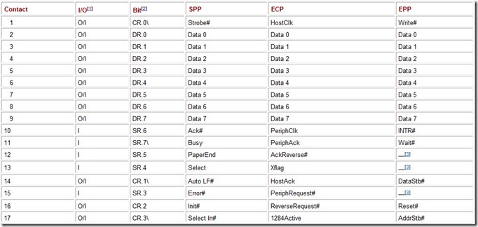
The traditional LPT port, called the Standard Parallel Port (SPP), is a unidirectional port for software implementation of the Centronics transfer protocol. (See Section 7.3.1). The names and the signal functions of the port connector conform to the Centronics interface (Table 1.1).
Table 1.1: Standard LPT Port Connector
[1]The I/O sets the direction of the port signal transmission (input/output). O/l denotes the output lines whose status is read when the output ports are read. O(I) denotes output lines whose status may be read only under special conditions.
[2]The \ character marks inverted signals. (Logical one in the register corresponds to the line’s low level.)
[3]The Ack# input is connected by a 10 Kohm resistor to the +5 V power supply.
An SPP adapter has three 8-bit registers occupying adjacent addresses in the I/O addressing space, starting from the port’s BASE address (3BCh, 378h, or 278h).
Data register (DR), address=BASE. Data written into this register are output to the Data [0:7] output lines. Data read out of this register, depending on the adapter circuit design, correspond either to previously written data or to the signals on the respective lines. These are not always the same.
Status register (SR) (read-only), address=BASE+1. This register represents the 5-bit input port of the printer status signals (bits SR. 4-SR.7) and the interrupt flag. The SR.7 bit is inverted: The value of logical one in the bit corresponds to the low-level signal, and vice versa.
The functions of the status register bits are as follows (with the pin number of the port connector in parentheses):
-
SR 7—Busy—Inverted reflection of the Busy (11) line status. When the line’s level is low, the bit is set to logical one, indicating permission to output the next byte.
-
SR. 6—Ack (Acknowledge)—Indication of the Ack# (10) line status.
-
SR. 5—PE (Paper End)—Indication of the PaperEnd (12) line status. The value of logical one corresponds to the line’s high level: the signal that the printer is out of paper.
-
SR. 4—Select—Indication of the Select (13) line status. The value of logical one corresponds to the line’s high level: The printer is online.
-
SR. 3—Error—Indication of the Error# (15) line status. The value of logical zero corresponds to the line’s low level: the signal of any printer error.
-
SR. 2—PIRQ—The Ack# interrupt flag (only for the PS/2 or Bi-Di port, see Section 1.2). It is set to logical zero if the Ack# signal causes a hardware interrupt. The value of logical one is set upon hardware reset and after reading the status register.
-
SR [1:0]—Reserved.
Control register (CR), address=BASE+2. This register can be written into and read from. The register is connected with the 4-bit output port for control signals (bits 0-3), which also may be read. The output buffer is usually an “open collector.” This allows this register’s lines to be used properly for input when they are programmed to the high level. Bits 0,1, and 3 are inverted.
The functions of the control register bits are as follows:
-
CR [7:6]—Reserved.
-
CR. 5—Direction—Transfer direction control bit (only for PS/2 or Bi-Di ports). A logical one written into the bit switches the port to the input mode. The bit status is undetermined during the register read operation.
-
CR. 4—AckINTEN (Acknowledge Interrupt Enable)—A value of logical one allows interrupts at the Ack# line’s trailing edge: the next-byte request signal.
-
CR. 3—Select In—A value of logical one in this bit corresponds to the low level on Select In# (17), the signal that allows the printer to work pursuant to the Centronics interface mode.
-
CR. 2—init—The bit’s zero value corresponds to the low level on the Init# (16) output: the hardware printer-reset signal.
-
CR. 1—Auto LF (Automatic Line Feed)—A value of logical one in this bit corresponds to the low level on the Auto LF# (14) output: the automatic line-feed signal upon receiving the carriage-return byte. Sometimes the signal and the bit are called AutoLF or AutoFDXT.
-
CR. 0—Strobe—A value of logical one in this bit corresponds to the low level on the Strobe# (1) output: the output-data strobe signal.
A hardware-interrupt request (usually IRQ7 or IRQ5) is generated upon the negative signal edge on pin 10 of the interface connector (Ack#) when CR. 4=1. To avoid false interrupts, pin 10 is connected through a resistor to the +5 V line of the bus. Interrupts are generated when the printer confirms that it has received the previous byte. As previously mentioned, BIOS neither uses nor services this interrupt.
The following steps output a byte using the Centronics interface (and the necessary number of processor-bus operations):
-
Write a byte to the data register (one IOWR# cycle).
-
Read the status register and check the device readiness (bit SR. 7, the busy signal). This step is repeated until either the ready signal is received or the software timeout is triggered (minimum one IORD# cycle).
-
Upon receiving the ready signal, the data strobe is set by writing to the control register. The strobe is cleared by the next write operation. To switch only one bit (strobe), the control register usually is read beforehand, which adds an extra IORD# cycle to the two IOWR# cycles.
To output 1 byte, four or five I/O port register operations are needed. (This is in the best-case scenario, when the printer’s readiness to receive a character is detected at the first reading of the status register.) This leads to the major shortcoming of using the standard port for output: low transfer rates accompanied by significant processor loading. Loading the processor to its capacity, the port can be accelerated to between 100 KBps and 150 KBps, not enough for output to a laser printer. The other shortcoming of the port is functional: the complexity of using it as an input port.
The standard port is asymmetrical. Twelve lines (and bits) usually output data; only five status lines input data. If a symmetrical bidirectional connection is needed, all standard ports are capable of working in the nibble (transfer) mode. In this mode, also called Hewlett-Packard Bitronics, 4 data bits are received simultaneously, and the fifth line is used for acknowledgement. This way, it takes two cycles to receive 1 byte, and every cycle requires at least five I/O operations.
The circuit design of the data output buffers of the LPT ports varies greatly. On many older adapters, the SPP data register also may be used to input data. If you write an all-ones byte into the port’s data register and place code on the port’s output lines using open-collector integrated circuits (or connect some lines to the circuit ground), this code can be read from the same data register. However, the output circuits of the information transmitter will have to “fight” the output current of logical ones from the output buffers of the adapter. TTL circuitry does not prohibit this approach because the electric current of an output contact that short-circuits to the ground usually does not exceed 30 milliamperes. However, if the external device is built on CMOS integrated circuits, these circuits may not have enough power to gain the upper hand in this struggle for the bus. Moreover, many modern adapters often have a matching resistor, up to 50 ohms, in their output circuits. A simple calculation shows that even if a pin short-circuits to the ground, during the output of a logical one, the voltage on this resistor will drop to 1.5 V. This means the receiver’s input circuit will interpret it as a logical one, not as a logical zero. Therefore, do not assume that such an input method will work on all computers. On some older port adapters, the output buffer may be disconnected by a jumper on the card. Then, the port turns into a simple input port.
1.2 Parallel Port Enhancements
The standard port’s shortcomings were partially eliminated by new kinds of ports that appeared in PS/2 computers.
Bidirectional Type 1 port (Type 1 parallel port). This interface was introduced in the PS/2. In addition to the standard mode, this kind of port can work in the input or bidirectional mode. The transfer protocol is software-generated, and to control the direction of the transfer, a special bit, CR.5, was added to the port’s control register. When it is set to logical zero, the data buffer is used for output; this buffer is used for input when this bit is set to logical one. Do not confuse this port, also called enhanced bidirectional, with the EPP. The Type 1 port has taken root in conventional PCs; it is called PS/2 or Bi-Di in SMOS Setup.
Direct memory access port (Type 3 DMA parallel port). This port was used in PS/2 models 57, 90, and 95. It was introduced to increase the data-transfer rate and to unload the processor during data output to the printer. Software working with this port only needed to define in the memory the data block to be printed. The output under the Centronics transfer protocol was conducted without the processor’s participation.
Later, other LPT port adapters were developed with the hardware implementation of the Centronics transfer protocol, or Fast Centronics. Some of them used the First In, First Out (FIFO) data buffer, or parallel port FIFO mode. Being nonstandardized, such ports from different manufacturers needed their own special drivers. Software directly controlling the standard port registers could not use their expanded capabilities. Ports of this type were often a part of the VLB multicards. They also have been built on ISA bus cards and into motherboards.
1.3 IEEE 1284 Standard
The IEEE 1284 parallel interface standard, adopted in 1994, describes the SPP, EPP, and ECP. The standard defines five modes of data transfer, a method for the host and the peripheral to determine the supported modes and negotiate to the requested mode, and the physical and electrical interfaces. In accordance with the IEEE 1284 standard, the following parallel-port data-transfer modes are possible:
-
Compatibility mode—A forward (output) unidirectional 8-bit channel with the Centronics protocol, software-controlled by the host. This is the port’s default mode: The port assumes it at the initialization and between all mode changes.
-
Half-byte (nibble) mode—A reverse (input) unidirectional, parallel-serial 4-bit channel, software-controlled by the host. It complements the compatibility mode but cannot work simultaneously with it. Switching is controlled by the host.
-
Byte mode—A reverse (input) unidirectional 8-bit channel, software-controlled by the host. It complements the compatibility mode but cannot work simultaneously with it. The host controls the switching.
-
EPP mode—A bidirectional 8-bit channel controlled by the processor, with hardware-implemented interlocked handshaking. Separate strobe lines distinguish between data and address transmissions.
-
ECP mode—A bidirectional, symmetrical 8-bit channel with hardware-implemented interlocked handshaking. A control line distinguishes between data and address transmissions; commands can be used to compress data and to address channels.
The standard defines the method by which software may determine the mode available to the host (a PC) and the peripheral device (or another connected computer). Nonstandard port modes using the Centronics data-transfer protocol via hardware (Fast Centronics, parallel port FIFO mode) may not be IEEE 1284 modes, despite their EPP and ECP features.
On the computers with the LPT port built into the motherboard, the SPP, EPP, or ECP mode, or a combination, is set in BIOS Setup. The compatibility mode is fully compatible with the SPP. The other modes are considered in the sections that follow.
In the descriptions of the modes, the following terminology is used:
-
Host—A computer with a parallel port
-
Ptr—In the names of signals, it means the transmitting peripheral device
-
Forward channel—A data-transfer channel from the host to a peripheral device
-
Reverse channel—A data-transfer channel to the host from a peripheral device
1.3.1 Half-Byte (Nibble) Mode
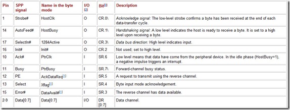
The half-byte mode is intended for bidirectional data-transfer and can work on all standard ports. Ports have five status-input lines. The peripheral device can use these to send a byte to the host 4 bits at a time in two actions. (A “nibble” is half of a byte, or 4 bits.) The Ack# signal that produces the interrupt, which may be used in the given mode, corresponds to bit 6 of the status register. This complicates software manipulations with the bits when assembling the byte. The port signals are given in Table 1.2; the timing diagrams are in Fig. 1.1.
Table 1.2: LPT Port Signals in the Nibble Input Mode
Receiving 1 byte in the half-byte mode involves the following steps:
-
The host signals its readiness to receive data by setting the HostBusy line to low.
-
In response, the peripheral device places a nibble on the input status lines.
-
The peripheral device signals that a nibble is ready by setting the PtrClk line to low.
-
The host sets the HostBusy line to high, indicating it is receiving and processing the nibble.
-
The peripheral device responds by setting the PtrClk line to high.
-
Steps 1-5 are repeated for the second nibble, after which (at step 7) the peripheral device may signal that it has data for the host (select) or that the forward channel is busy (Busy). It also may trigger interrupts (Ack) at this time.
The interlocked handshaking is processed by the host via software (using CR and SR). Therefore, the transfer rate cannot be raised above 50 KBps. Its unarguable advantage is that it works with all ports. It is used when the volume of the data stream is not large (such as for communicating with printers). When communicating with local area network (LAN) adapters, external disk-storage devices, or a CD-ROM, receiving voluminous data requires ample patience from the user.
1.3.2 Byte Input Mode
In this mode, data are received using the bidirectional port whose buffer may be turned off by setting the CR. 5 bit to logical one. Like the preceding modes, it is software-controlled: all handshaking signals are analyzed and set by the driver. The port signals are described in Table 1.3; the timing diagram is given in Fig. 1.2.
Table 1.3: LPT Port Signals in the Byte Mode
[2]I/O sets the direction of the port signal transmission (input/output).
[3]The \ character marks inverted signals. (Logical one in the register corresponds to the line’s low level.)
[1]Signals follow the negotiation sequence
The stages of receiving a byte are as follows:
-
The host signals its ability to receive data by setting the HostBusy line to low.
-
In response, the peripheral device places a byte of data on the Data [0:7] lines.
-
The peripheral device signals that the byte is valid by setting the PtrClk line to low.
-
The host sets the HostBusy line to high, indicating it is receiving and processing the byte.
-
The peripheral device responds by setting the PtrClk line to high.
-
The host acknowledges the byte has been received by pulsing the HostClk line. Steps 1-6 are repeated for each following byte. After the HostBusy line goes high (step 4), the peripheral device may signal that it has data for the host (DataAvail#), that the forward channel is busy (PtrBusy), and generate interrupts when the data is ready (PtrClk).
The interlocked handshaking implemented by the HostBusy and PtrClk signals is processed by the host using software (using the CR and SR registers). The peripheral device may not necessarily use the HostClk signal (this is an invitation to send another byte). Speeds on a par with those of the forward channel can be achieved (up to 150 KBps). However, this mode can only function in bidirectional ports, which early on used to be exploited mainly on rarely encountered PS/2 machines. Most modern ports can be configured into the bidirectional mode (using Bi-Di or PS/2 in BIOS Setup).
However, this mode can function only in bidirectional ports. Early on, these were used mainly on rare PS/2 machines. Most modern ports can be configured into the bidirectional mode (using Bi-Di or PS/2 in BIOS Setup).
1.3.3 EPP Mode
The Enhanced Parallel Port (EPP) protocol was developed by Intel, Xircom, and Zenith Data Systems long before the IEEE 1284 standard was accepted. This protocol is intended for increasing data-transfer efficiency of the parallel port. It was first implemented in the Intel 386SL chipset (IC 82360); later, it was adopted by many companies as an optional parallel-port data-transfer protocol. There are some deviations from EPPs before IEEE 1284 in the current IEEE 1284 EPP standard.
The EPP protocol provides four types of data-transfer cycles:
-
Data Write Cycle
-
Data Read Cycle
-
Address Write Cycle
-
Address Read Cycle
The data-exchange cycles differ from the address cycles in the strobe signals that they use. The purpose of the write and read cycles is obvious. Separating the address cycles makes it possible to connect devices with multiple registers by organizing a multiplexed address and data bus. Table 1.4 describes the EPP signals and their correlation with the SPP signals.
Table 1.4: LPT Port Signals in the EPP Mode
2]I/O sets the direction of the port signal transmission (input/output).
[1]Signals follow the negotiation sequence.
The EPP has an expanded register set (Table 1.5) that occupies 5-8 contiguous bytes in the I/O addressing space.
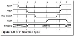
Unlike in the software-controlled modes described previously, the external signals of the EPP are hardware-generated for each exchange cycle by a single CPU I/O instruction, addressed to the EPP data or address register. In the previously considered modes, the external exchange cycle was formed by a sequence of I/O operations. Fig. 1.3 shows a diagram of the data-write cycle. It illustrates an external exchange cycle, embedded in a processor system-bus write cycle. (These cycles sometimes are called interlocked.) The address-write cycle differs from the data-write cycle only in its external interface strobe.
The data-write cycle consists of the following phases:
-
The program executes an I/O write cycle (IOWR#) to port 4 (EPP Data Port).
-
The adapter sets the Write# signal (low level), and the data are placed onto the parallel-port output bus.
-
With the Wait# signal low, the data strobe is set.
-
The port waits for acknowledgement from the peripheral device (switching Wait# to high).
-
The data strobe is cleared, and the external EPP cycle ends.
-
The output cycle of the processor ends.
-
The peripheral device sets the Wait# signal to low to indicate that the next cycle may begin.
An example of an address-read cycle is given in Fig. 1.4. The data-read cycle differs only in that it uses a different strobe signal.
The distinguishing feature of the EPP is the entire data transfer occurs within one processor I/O cycle. This allows high transfer rates (from 500 KBps to 2 MBps) to be achieved. A peripheral device connected to the EPP can operate at the performance levels of a device connected via the ISA bus slot. The interlocked handshake protocol allows the automatic establishment of a transfer rate that both the host and the peripheral device support. The peripheral device can control the duration of all the data-exchange phases using only the Wait# signal. The protocol automatically adjusts to the cable length: Introduced delays will only lengthen the cycle. Cables that comply with the IEEE 1284 standard have the same wave characteristics for different types of lines; therefore, transmission breaks because of “competition” between the signals should not occur. An interesting phenomenon may be observed when network adapters or external drives are connected to the EPP: As the length of the interface cable increases, the productivity drops.
Naturally, the peripheral device must not “hang” the processor during the bus cycle of the transfer. This is guaranteed by the computer’s timeout mechanism, which ends any exchange cycle that lasts more than 15 microseconds (μsec). In a series of EPP implementations, the adapter watches the interface timeout: If the peripheral device does not answer in 5 μsec, the cycle terminates and the adapter’s custom (nonstandard) status register records an error.
EPP devices based on the pre-IEEE 1284 protocol deviate in the beginning of the cycle: The DataStb# or Addrstb strobe signals are set regardless of the state of the Wait# signal. This means that the peripheral device cannot hold off the beginning of the next cycle (although the device can extend it as necessary). This specification is called EPP 1.7. (It was proposed by Xircom.) This version was used in the 82360 controller. Peripheral devices compatible with the IEEE 1284 EPP will work normally with an EPP 1.7 controller, but an EPP 1.7 peripheral device may refuse to work with an IEEE 1284 EPP controller.
From the software standpoint, an EPP controller looks simple. (See Table 1.5.) To the three registers of the standard port, with the 0, 1, and 2 offsets relative to the base port address, two more registers have been added (EPP Address Port and EPP Data Port). Reading from and writing into these registers generates interlocked interface cycles.
The traditional roles of the standard port registers have been preserved for compatibility between the EPP and peripheral devices and software designed to use software-controlled data exchange. The handshaking signals are hardware-generated by the adapter; therefore, when initiaizing EPP to the control register (CR), bits 0, 1, and 3 (corresponding to the strobe#, AutoFeed#, and Selectin# signals) must be set to logical zero values. Software intervention could distort the handshake sequence. Some adapters have special protections (EPP Protect) that can be turned on to block software modification of these bits.
Using the EPP data register allows a block of data to be transferred with one REP INSB or REP OUTSB instruction. Some adapters allow 16- or 32-bit access to the EPP data register. Here, an ISA adapter simply decodes the address with an offset in the 4-7 range as the EPP data register address. However, it tells the bus controller the address is 8 bits wide. This leads I/O addressing of the 16- or 32-bit EPP data register to generate automatically two or four 8-bit bus cycles, addressed in an increasing sequence that begins from the offset 4. All four cycles will be executed in less time than the same number of single cycles, each triggered by a 1-byte I/O instruction. More advanced adapters have an “honest” 32-bit data register. For them, up to 4 bytes may be transferred by one processor instruction in one bus cycle. This way, transfer rates up to 2 MBps may be achieved, sufficient for LAN adapters, external disc drives, streamers, and CD-ROM drives. EPP address cycles are always executed in 1-byte mode.
An important feature of the EPP is that the processor accesses the peripheral device in real time: Data are not buffered. The peripheral driver is able to determine the state of and to control the communications. The read and write cycles may follow randomly or in blocks. This type of exchange is practical for register-oriented or real-time peripheral devices, such as data-collecting and -control devices. This mode of data transfer also is suitable for data storage devices, LAN adapters, printers, scanners, etc.
Unfortunately, not all ports support the EPP mode; several types of notebook PCs don’t have it. Therefore, when developing custom devices, it is necessary to try using the ECP mode to achieve greater compatibility with computers.
1.3.4 ECP Mode
The ECP protocol was proposed by Hewlett-Packard and Microsoft to communicate with peripheral devices such as printers or scanners. Like the EPP protocol, this protocol provides high-performance bidirectional data exchange between a host and a peripheral device.
The ECP provides two forward and reverse cycles:
-
Data-read and -write cycles
-
Command cycles
The command cycles are subdivided into two types: channel-address transmission and Run-Length Count (RLC) transmission.
Unlike the EPP, the standard on the software (register) implementation of the ECP adapter was introduced with the ECP protocol. It is described in the Microsoft document The IEEE 1284 Extended Capabilities Port Protocol and ISA Interface Standard This document defines protocol features not addressed by the IEEE 1284 protocol:
-
Data compression by the host adapter using the Run-Length Encoding (RLE) method
-
FIFO buffering for the forward and reverse channels
-
DMA and programmed I/O usage
The real-time RLE data-compression feature enables compression ratios up to 64:1 when transmitting raster images that have long strings of identical data. The compression feature can be used only if both the host and the peripheral device support it.
ECP channel addressing is used to address multiple logical devices within a single physical device. For example, in a joint fax/printer/modem device with a single parallel port, it is possible to receive a fax and print simultaneously. In the SPP mode, if the printer sets the busy signal, the channel will be kept busy with data until the printer receives them. With the ECP mode, the software driver simply addresses another logical channel of the same port.
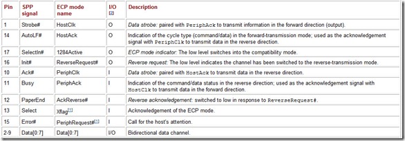
The ECP protocol redefines the SPP signals (Table 1.6).
Table 1.6: LPT Port Signals in the ECP Mode
[2]I/O sets the direction of the port signal transmission (input/output).
[1]Signals follow the negotiation sequence.
An ECP adapter also generates external handshaking signals using hardware, but it works differently from the EPP mode.
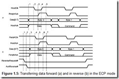
Fig. 1.5, a, shows two forward-transfer cycles: The data cycle is followed by the command cycle. The cycle type is set by the level on the HostAck line: high for data, low for a command. During the command cycle, the byte may contain the channel address or the RLE counter. The distinction is made by bit 7 (i.e., the topmost bit): If it is low, bits 0-6 contain the RLE counter (0-127); if it is high, they contain the channel address. Fig. 1.5, b, shows two reverse-transfer cycles.
Unlike the EPP mode transfer diagrams, Fig. 1.5 does not show the signals for the processor system-bus cycles. In this transfer mode, the driver-to-peripheral-device exchange is broken into two relatively independent processes, connected via the FIFO buffer. The driver-to-FIFO-buffer exchange may be performed using DMA and the software I/O. The peripheral-device-to-buffer exchange is accomplished using the ECP adapter. The driver in the ECP mode does not have the information about the exact state of the exchange process; however, the only thing that matters usually is whether or not it has been completed.
Forward transmission of data on the external interface consists of the following steps:
-
The host places data on the data lines and indicates either a data cycle (high level) or a command cycle (low level) on the HostAck line.
-
The host sets the HostClk line to low, indicating valid data.
-
The peripheral device responds by setting the PeriphAck line to high.
-
The host sets the HostClk line to high. This edge may be used to clock the data into the peripheral device.
-
The peripheral device sets the PeriphAck line to low, indicating it is ready to receive the next byte.
Because ECP transfers are conducted via FIFO buffers, which may be present on both sides of the interface, it is important to understand at what stage data may be considered transferred. Data are considered transferred at Step 4, when the HostClk line goes to high. At this time, the counters of the sent and received bytes are updated. There are conditions in the ECP protocol that may cause the transfer of data to abort between Steps 3 and 4. In such a case, data should not be considered transferred.
Fig. 1.5 shows yet another difference between the ECP and EPP transfer modes. The EPP protocol allows the driver to intermix the forward- and reverse-transfer cycles without asking for acknowledgement to switch direction. With the ECP, direction change must be negotiated. The host must request the reverse channel-transfer by setting the ReverseRequest# line. Then, it must wait for the peripheral to acknowledge the request by setting the AckReverse# line. Because the previous transfer cycle may have been performed using DMA, the driver must either wait for DMA to complete or interrupt it, back-flush the FIFO buffer to determine the exact value of the transferred bytes counter, then request the reverse channel.
Reverse data-transfer consists of the following steps:
-
The host requests the channel direction change, setting the ReverseRequest# line to low.
-
The peripheral device allows the direction change by setting the AckReverse# line to low.
-
The peripheral device places data on the channel bus and indicates the nature of the cycle by setting the PeriphAck line to high (a data cycle) or low (a command cycle).
-
The peripheral device sets the PeriphClk line to high, indicating the data are valid.
-
The host responds by setting the HostAck line to high.
-
The peripheral device sets the PeriphClk line high; this edge may be used by the host to clock the data.
-
The host sets the HostAck line to low, indicating it is ready to receive the next byte.
1.3.5 ECP Modes and Registers
The software interface and ECP registers for IEEE 1284 adapters are defined by a Microsoft specification. The ECP can work in various modes, shown in Table 1.7. In this table, the code corresponds to the Mode field of the ECR register (bits [7:5]).
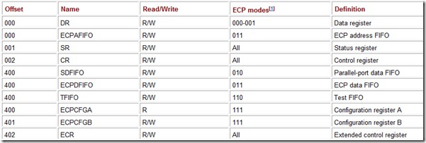
The ECP adapter register model (Table 1.8) takes advantage of a peculiarity of the ISA for the bus and adapters: Only the ten low-order address bus lines are used to decode I/O port addresses. As a result, addressing Port, Port+400h, Port+800h, etc., will be interpreted as addressing Port in the 0-3FFh range. Modern PCs and adapters decode addresses consisting of numerous bits; therefore, addressing 0378h and 0778h will address two separate registers. Placing two additional ECP registers “behind” the standard port registers (offset 400h-402h) achieves two goals. First, these addresses have never been used by traditional adapters or their drivers, and their use in the ECP will not narrow the available I/O addressing space. Second, this provides compatibility with older adapters on the level of 000-001 modes and the possibility of determining whether an ECP adapter is present by trying to access its extended registers.
Every ECP mode has corresponding (and accessible) function registers. The mode is switched by a write into the ECR register. The “on-duty” modes, enabled by default, are 000 and 001. The half-byte input mode functions in either of them. It is always possible to switch from these modes into any other mode. However, from the higher modes (010-111), switching only is possible into the 000 or 001 mode. To ensure that the interface works correctly, it is necessary to wait until the DMA transfer has been concluded and the FIFO buffer has been cleared.
000 (SPP) mode. The port works as the unidirectional software-controlled SPP.
001 (Bi-Di PS/2) mode. The port works as bidirectional, Type 1 PS/2 port. The difference between this and the 000 mode is that the 001 mode can use the CR. 5 bit to reverse the data channel.
010 (Fast Centronics) mode. This mode is intended only for high-efficiency output through the FIFO buffer using DMA. The handshake signals for the Centronics protocol are hardware-generated. The interrupt-request signal is based on the state of the FIFO buffer, not the Ack# signal. (The high-speed block-transfer driver is not “interested” in a request from a single byte.)
011 mode. This is actually the ECP mode described previously. The stream of data and commands transmitted into the peripheral device is placed into the FIFO buffer using the ECPDFIFO and ECPAFIFO buffers, respectively. They are output from the FIFO upon the corresponding indication of the cycle (i.e., the state of the HostAck line). The stream of data received from the peripheral device is extracted from the FIFO buffer using the ECPDFIFO register. Receiving address information from the peripheral device in the command cycle is not planned. Exchange with the ECPDFIFO register also can be conducted via the DMA channel.
100 mode (EPP). This is one method that enables the EPP mode (if it is supported by the adapter and enabled in CMOS Setup).
110 mode (test mode). This mode is intended for testing the interaction between the FIFO and interrupts. Data may be transmitted in and out of the TFIFO register using DMA or software. The exchange does not affect the external interface. The adapter executes dummy operations, without actual external cycles, working at the interface maximum speed (as if the handshake signals were coming through without delays). The adapter monitors the buffer state and generates interrupt-request signals as necessary. This way, the driver can determine the maximum throughput capacity of the channel.
111 mode (configuration mode). This mode is intended to provide access to the configuration registers. Making this a separate mode protects the adapter and the protocol from erroneous configuration changes during the exchange process.
RLE method compression in ECP mode. During the forward transfer, this compression is done by software. To transmit more than two identical bytes in a row, the ECPAFIFO register is loaded with a byte whose first seven low-order bits contain the RLC counter and whose topmost bit is set to logical zero. (The RLC value of 127 corresponds to 128 repeats.) Then, the byte is loaded into the ECPDFIFO register. The peripheral device performs decompression when it receives this pair of bytes (i.e., the command byte and the data byte). Receiving a stream of data from a peripheral device, an ECP adapter performs decompression using hardware and places into the FIFO buffer already decompressed data. This makes it obvious that it is impossible to output data using compression and DMA simultaneously.
As previously mentioned, each ECP mode has a corresponding function register (Table 1.8).
The data register (DR) is used to transmit data only in the software-controlled modes (000 and 001).
The status register (SR) transmits the values of the signals on the corresponding lines (as in the SPP).
The function of the bits in the control register (CR) coincides with that of the SPP. In the 010 and 011 modes, writes into bits 0 and 1 (the AutoLF# and Strobe# signals) are ignored.
The ECPAFIFO register is used to place command cycle information (the channel address or RLE counter, depending on the value of bit 7) into the FIFO buffer. The information is output from the buffer during the command cycle of the output.
The SDFIFO register is used to transfer data in the 010 mode. Data that have been written into the register (or sent via the DMA channel) are sent through the FIFO buffer using the hardware-implemented Centronics protocol. The transfer direction should be set to forward in this mode (i.e., the CR. 5 bit should be set to 0).
The DFIFO register is used to exchange data in the 011 mode (ECP). Data that have been written into or read from the register (or transmitted via the DMA channel) are transmitted through the FIFO buffer under the ECP protocol.
The TFIFO register provides the FIFO buffer testing mechanism in the 110 mode.
The ECPCFGA register allows information about the adapter to be read (i.e., the identification code in bits [7:4]).
The ECPCFGB register allows any information required by the driver to be saved. Writing into the register does not affect the port’s functionality.
The ECR register is the main ECP control register. Its bits have the following functions:
-
ECR [7:5]—ECP MODE—Sets the ECP mode.
-
ECR. 4—ERRINTPEN# (Error Interrupt Disable)—Disables interrupts at the Error# signal. (If this bit has the value of logical zero, the falling edge on the Error# line causes an interrupt to be generated).
-
ECR. 3—OWEN (DMA Enable)—Enables DMA channel exchange.
-
ECR. 2—SERVICEINTR (Service Interrupt)—Disables service interrupts that were generated upon completion of the DMA cycle (if it is enabled), at the FIFO buffer filling or emptying threshold (if the DMA is not being used), and at the buffer overflow or underfiow error.
-
ECR. 1—FIFOFS (FIFO Full Status)—Signals that the buffer has been filled. When FIFOFS=1, the buffer has no free space.
-
ECR. 0—FIFOES (FIFO Empty Status)—Indicates that the buffer is empty. The FIFOFS=FIFQES=1 combination indicates an FIFO error (underfiow or overflow).
When the port is in the standard or bidirectional mode (000 or 001), the first three registers coincide with the standard port registers. This way, the compatibility of new drivers with old adapters and of old drivers with new adapters is ensured.
In its interface with the driver, the ECP resembles the EPP: After a mode has been set (i.e., a code written into the ECR register), data exchange with the device comes to reading from or writing to the appropriate registers. The FIFO buffer status is monitored by using the ECR register or by processing the service interrupts from the port. The entire handshake protocol is hardware-generated by the adapter. Data exchange with the ECP (except for software-implemented exchange) is possible through the DMA channel. This channel is effective when transmitting large blocks of data.
1.3.6 IEEE 1284 Negotiation
An IEEE 1284 standard peripheral device does not usually require the controller to implement all the modes provided by this standard. To determine the modes and methods used to control a device, the standard provides a negotiation sequence. The sequence’s construction keeps older devices that do not support IEEE 1284 from responding to it; with these devices, the controller remains in the standard mode. Peripheral devices that support IEEE 1284 can provide information about their capabilities. The controller will set the mode acceptable to both the host and the peripheral device. All mode switching is conducted through negotiation.
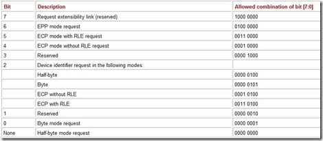
During the negotiation phase, the controller places the extensibility byte on the data lines, requesting an acknowledgement to switch the interface into the required mode or asking for a peripheral device identifier (Table 1.9). The identifier is relayed to the controller in the requested mode (i.e., any reverse-channel mode, except the EPP mode). The peripheral device uses the xflag signal (Select in SPP terminology) to confirm the requested reverse-channel mode. The exception is the half-byte mode, supported by all IEEE 1284 devices. The Extensibility Link request bit is intended for determining additional modes in future extensions of the standard.
Table 1.9: Bit Values of the Extensibility Byte
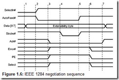
The negotiation sequence (Fig. 1.6) consists of the following steps:
-
The host places the extensibility byte on the data lines.
-
The host sets the SelectIn# line to high and the AutoFeed# line to low, starting the negotiation sequence.
-
The peripheral device responds by setting the Ack# line low and the Error#, Paper-End, and Select lines high. A device that does not “understand” the IEEE 1284 standard will not respond, and further steps will not be carried out.
-
The host sets the Strobe# signal to low to write the extensibility byte into the peripheral device.
-
The host sets the Strobe# and AutoLF# signals to high.
-
If the peripheral device has data for transmission by the reverse data-transfer channel, it responds by setting the PaperEnd and Error# signals to low. If the device supports the requested mode, the Select line is to set high; if it doesn’t provide support, the line is set to low.
-
The peripheral device sets the Ack# line to high, indicating the end of the negotiation sequence. After this, the controller sets the required work mode.
1.3.7 Physical and Electrical Interfaces
The IEEE 1284 standard defines the physical characteristics of the receivers and transmitters of TTL level-compatible signals. The standard port specifications did not define the types of output circuits, the limit values of load resistors, or the capacities introduced by circuits and conductors. At relatively low transfer rates, this parameter spread did not cause compatibility problems. However, the extended modes (in functions as well as in transfer rate) demand explicit specifications. The IEEE 1284 standard defines two levels of interface compatibility. The Level I interface is defined for devices that operate at low transfer rates but use the reverse-channel capabilities. The Level II interface is defined for devices that operate in the extended mode at high transfer rates and are connected by long cables. The following requirements are set for the Level II transmitters:
-
Open-circuit signal-voltage levels shall fall between −0.5 V and +5.5 V.
-
Signal voltage levels at the steady load current of 14 milliamperes shall be no less than 2.4 V for the high level (VOH) and no higher than 0.4 V for the low level (VOL).
-
The output impedance (RO), measured at the connector, shall be 50±5 ohms at the VoH−VOL level. To provide the required impedance, resistors connected in series are used in the output circuits of the transmitter. Matching the impedances of the transmitter and the cable lowers the level of impulse distortions.
-
The pulse rise (drop) rate shall be within 0.05 V/nsec and 0.40 V/nsec.
The requirements for the Level II receivers are as follows:
-
Tolerable peak values of the signals shall be between −2 V and +7 V.
-
Threshold voltages shall be no higher than 2.0 V (VIH) for the high level and no lower than 0.8 V (VIL) for the low level.
-
A receiver shall have a hysteresis no lower than 0.2 V and no higher than 1.2 V. (Special integrated circuits known as Schmidt triggers have hysteresis.)
-
The input current of an integrated circuit shall not exceed 20 microamperes. The input lines are connected to the +5 V power bus by a 1.2 K resistor.
-
The output capacitance shall not exceed 50 picofarad (pF).
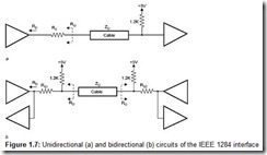
When the ECP specification was first introduced, Microsoft made a recommendation that dynamic terminators be used on each interface line. Nevertheless, an IEEE’ 1284 specification that does not call for dynamic terminators is followed today. Fig. 1.7 shows diagrams of some recommended schematics for the input, output, and bidirectional circuits.
The IEEE 1284 standard defines three types of connectors. Types A (DB-25) and B (Centronics-36) are characteristic of traditional printer-interface cables. Type C is a new, compact 36-contact connector.
Traditional interface cables have between 18 and 25 wires, depending on the number of GND (ground) circuit wires. These conductors may be twisted. No strict requirements were made for the cable shielding. It is unlikely that such cables will work reliably at a transfer rate of 2 MBps or at a length greater than 6.5 feet.
The IEEE 1284 standard regulates cable characteristics.
-
All signal lines shall be twisted with separate return (common) lines.
-
Each pair shall have an impedance of 62±6 ohms in the frequency range of 4 MHz to 16 MHz.
-
The noise level of cross talk between the pairs shall not exceed 10%.
-
The cable shall have a shield (foil) that covers no less than 85% of the outer surface. At each end, the cable shall be connected to the connector backshell using a 360-degree concentric method.
Cables meeting these requirements are marked “IEEE Std 1284-1994 Compliant.” They may be as long as 32 feet. The available assembly types are listed in Table 1.10.
Table 1.10: IEEE 1284 Cable Types
Additions to the main IEEE 1284 standard include the following:
-
IEEE P1284.1 (Standard for Information Technology for Transport-Independent Printer/System Interface (TIP/SI))—Transport-independent host/printer interaction through a bidirectional interface based on the Network Printing Alliance Protocol (NPAP).
-
IEEE P1284.2 (Standard for Test, Measurement and Conformance to IEEE Std. 1284)—Testing devices, ports, and cables for compliance with IEEE1284.
-
IEEE P1284.3 (Standard for Interface and Protocol Extensions to IEEE Std. 1284 Compliant Peripheral and Host Adapter Ports)—Interface and protocol port and 1284 device extensions for transparent work with multiple devices connected to the port in daisy chains and via multiplexers. Additional modes are Block ECP (BECP) and Channelized Nibble modes (using ECP channel addressing for half-byte mode).
-
IEEE P1284.4 (Standard for Data Delivery and Logical Channels for IEEE Std. 1284 Interfaces)—A packet protocol for data transport and logical channel organization for 1284 devices. Corresponds to the transport and session layers of the OSI model; can work above the 1284.3 channel layer. Provides link establishment, configuration, flow control and data transfer, as well as service detection for port clients.
1.4 LPT Port System Support
System support of the LPT port includes a search for the installed ports and provides Int17h print services. (See Section 7.3.3.) During the initial POST testing, BIOS checks for parallel ports at the 3BCh, 378h, and 278h addresses. It places the BASE addresses of the ports it finds into the BIOS Data Area cells: 0:0408h, 0:040Ah, 0:040Ch, and 0:040Eh. These cells store the LPT1-LPT4 port addresses. The value of logical zero in these cells means there is no port with such a number. Cells 0:0478h, 0:479h, 0:47A, and 0:47Bh store the constants that set the timeouts for these ports.
Most port searches are conducted inefficiently: A test byte (AAh or 55h) is output to the BASE address (into the data register of the supposed port). Then, an input is made from the same address. If the written and the read bytes match, an assumption is made that the LPT port has been found. The address is placed into the BIOS Data Area cell. Subsequently, the port’s BASE addresses may be modified by software. BIOS cannot determine the LPT4 port address on its own; the list of standard addresses only contains the three previously mentioned addresses.
Ports that have been found are initialized: Through a write operation into the control register, the Init# signal is activated and negated. Then, the value of OCh is written, which corresponds to the initial state of the interface signals. In some cases, the Init# signal is active from the moment the hardware is reset until port initialization during the loading of the operating system. This may be detected by the printer behavior during system reboot: Its online light goes and stays off for a long time. As a result, it becomes impossible to print screens (such as the BIOS Setup parameters) by pressing the <Print Screen> key before the operating system has been loaded.
EPP BIOS functions were introduced to provide support for the port modes defined in IEEE 1284. Before these functions can be used, the presence of EPP BIOS must be checked (not all BIOS versions have EPP functions). This Installation Check is done by using function 2 of Int 17h (querying the LPT status) with the keyword EPP loaded into the CH, BL, and BH registers. If the BIOS contains EPP functions, this call will return their entry point. EPP BIOS provides the following functions:
-
Query Config—getting port address, interrupt number and port capabilities (version and modes available)
-
Get/Set Mode—detecting and setting the current mode (SPP, BiDi, ECP, EPP, EPP 1.7)
-
Interrupt Control—enabling and disabling interrupt use
-
EPP Reset—resetting port
-
Executing exchanges in the EPP mode: single address and data read/write cycles; data block input or output; combined operations (sending an address and inputting or outputting a byte or a data block)
-
Lock/Unlock Port—selecting and Locking/Unlocking a device connected in chain or via a multiplexer
-
Device Interrupt—installing interrupt handlers for the specified devices connected in chain or via a multiplexer.
-
Check INT Pending—determining the device interrupt source
-
Multi-Port Extensions—additional functions for working with multiplexers and chains: polling (version, current port selected, locking, interrupt); polling the selected port status; polling the chain (determining the selected device and its status); setting identifiers for devices that cannot communicate them themselves
1.5 Parallel Port and Plug-and-Play Functions
Most modern peripheral devices connected to the LPT port support the IEEE 1284 standard and plug-and-play functions. To support these functions, all the computer needs on the hardware side is an IEEE 1284-compliant interface controller. If the connected device supports plug-and-play, using the IEEE 1284 negotiation sequence, it can “arrange” possible exchange modes with the port that represents computer “interests.” For plug and play to work, the connected device must present all the necessary information about itself to the operating system. At the minimum, there are the identifiers of the manufacturer, the model, and the set of supported commands. Detailed information about the device may contain the class identifier, a description and identifier of a brand-name device with which the given device is compatible. Based on the obtained information about the support for the specific device, the operating system may attempt to install the required software.
Devices supporting plug and play are recognized by the operating system during the boot stage—if they are connected to the port by the interface cable and powered up. If Windows detects a connected plug-and-play device that differs from the one recorded in its registry, it tries to install the drivers needed by the device from the OS distribution kit or from the new device’s software-installation package. If Windows does not want to see the newly connected plug-and-play device, it may be an indication that the port or the cable is out of order. The plug-and-play system will not work if the device is connected by a cheap non-bidirectional cable that does not provide connection through the selectin# line (e.g., contact 17 on the LPT port and contact 36 on the Centronics connector).
1.6 Uses of the LPT Port
Usually, the LPT port is used to connect a printer. (See Section 7.3.1.) Its use is not limited to this.
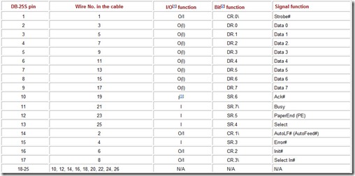
To connect two computers employing the parallel interface, various cables are used, depending on the modes of the ports. The simplest and the slowest is the half-byte mode, which works in all ports. To use this mode, the cable only needs to have ten signal conductors and one common conductor. Table 1.11 shows the contact wiring for the cable connector. PC communication over this cable is supported by standard software, such as MS-DOS Interlink or Norton Commander. Note that a proprietary protocol is used, differing from the one described in Section 1.3.1.
Table 1.11: Computer-Computer Connection Cable (4 bits wide)[
Two computers can maintain a high rate of communication in the ECP mode. (The EPP mode is not convenient; it requires the bus I/O cycles of the computers to be synchronized).
Table 1.12 shows cable wiring for this mode. Of all the signals in the cable, only PeriphRequest# (contact 15) is not used. It is recommended that series resistors (0.5-1 Kohm) be put into the data-line circuits. They will prevent currents that are too strong from flowing through these lines when the ports of both computers are in the output mode. Such a situation can arise when the computer’s communication software has not been launched yet. ECP mode communication is supported by Windows 9x in its distribution kit, a PARALINK. VXD driver is included. However, because of a programming error, it does not work and needs to be patched. A patch for this driver, a test utility, and the necessary instructions can be found at the following Web sites: http://www.lpt.com and http://www.lvr.com/parport.htm.
Table 1.12: Computer-Computer 8-bit Communication Cable
Connecting a scanner to the LPT port is effective only if the port provides at least the bidirectional mode (Bi-Di), because the prevailing data stream is reverse. It is better to use the ECP, if the scanner supports this mode (or the EPP, which is unlikely).
The connection of external data-storage devices (Iomega Zip drive, CD-ROM, etc.), LAN adapters, or other symmetrical I/O devices has its own peculiarities. In the SPP mode, such connections slow down the device performance. In addition, the fundamental asymmetry of this mode becomes noticeable: Data are input at half the rate of their output (which is slow enough). The bidirectional mode (Bi-Di or PS/2 Type 1) eliminates this asymmetry: The transfer rates become equal. Only by switching into the EPP or ECP mode can normal transfer rates be obtained. The LPT port connection in the EPP or ECP mode has almost the same connection speed as an ISA controller connection. This is also true when the standard bus interface devices are connected to the LPT ports using interface adapters (such as LPT-to-IDE, LPT-to-SCSI (Small Computer System Interface), or LPT-to-PCMCIA (Personal Computer Memory Card International Association)). Note that an IDE hard disk drive connected to the LPT port via an adapter can be presented to the system as an SCSI device. (This is more logical from the software standpoint.)
Table 1.13 gives a description of the LPT port connector contacts in different modes and their correspondence to the standard port register bits.
Table 1.13: Functions of the LPT Port Connector Contacts and Register Bits
1.7 Configuring LPT Ports
Parallel port control is split into two stages: preliminary configuration (setup) of the port’s hardware assets and extemporaneous switching (operational) of the operation modes by the application or system software. Operational switching is possible only within the limits of the modes enabled at the setup. It matches the equipment with the software and blocks false switches caused by incorrect program operations.
LPT port configuration depends on its physical implementation. A port located on an extension card (multicard) installed into an ISA or ISA+VLB bus is configured by jumpers on the card. A port built-in into the system board is configured by BIOS Setup.
The following port parameters are subject to configuration:
-
BASE address—3BCh, 378h, or 278h—During the initialization, BIOS checks for ports in this address order. Accordingly, it assigns the detected ports the following logical names: LPT1, LPT2, and LPT3. The 3BCh address is assigned to a port adapter located on an MDA or HGC. Most ports are configured by default to address 378h; they can be switched to 278h.
-
Interrupt request line—IRQ7 for the LPT1, and IRQ5 for the LPT2—Traditional printer-originated interrupts are not enabled, and this scarce resource can be spared. However, when working in a high transfer-rate ECP (or Fast Centronics) mode, interrupts can raise the transfer efficiency noticeably and decrease the processor workload.
-
DMA channel—ECP and Fast Centronics modes—The DMA and its channel number are enabled.
-
Port work modes:
-
SPP—The port only works in the standard unidirectional software-controlled mode.
-
PS/2 (or Bidirectional)—This differs from the SPP in its capability to reverse the channel (by setting CR. 5 bit to logical one).
-
Fast Centronics—This hardware generation of the Centronics protocol uses the FIFO buffer and possibly DMA.
-
EPP—Depending on how the registers are used, the port works in the SPP or EPP mode.
-
ECP—By default, the SPP or PS/2 mode is enabled. Writing into the ECR can switch into any ECP mode, but writing code 100 into the ECR cannot guarantee a switch into the EPP mode.
-
ECP+EPP—This is the same as the ECP, but writing code 100 into the ECR switches the port into the EPP mode.
-
Selecting the EPP, ECP, or Fast Centronics mode does not increase the datatransfer rate with the connected peripheral device; it only gives the driver and the peripheral device an opportunity to set the optimal mode within the limits of their “understanding.” Most modern drivers and applications attempt to use efficient modes; therefore, there is no need to “clip their wings” without a valid reason.
Printers and scanners may desire the ECP mode. Windows (3x, 9x, and NT) has system drivers for this mode. In the DOS environment, printing in the ECP mode is supported only by a separately loaded, custom ECP driver.
Network adapters, external disk drives, and a CD-ROM connected to the parallel port can use the EPP mode. No standard driver is available for this mode yet; its support is provided by the driver of the connected device.
1.8 Troubleshooting Parallel Port Malfunctions
It is sensible to begin troubleshooting parallel ports by checking whether they are present in the system. A list of installed port addresses is displayed on the monitor by BIOS before the operating system is loaded. The list may be inspected with the help of testing software or a debugger in-the BIOS Data Area.
If BIOS detects fewer ports than are installed, two ports likely have been assigned the same address. When this happens, there is no guarantee that conflicting ports will work. When data are written into the registers, the conflicting ports will put out signals simultaneously. However, reading of the status register will cause a bus conflict. This conflict likely will lead to data corruption. Testing a port without a diagnostic loop-back plug will not show errors; during such testing, data from the output registers are read and will be identical for all conflicting ports that separately are in working order. This kind of test is done by BIOS when it checks for the presence of ports. To resolve such a situation, install ports one by one, monitoring the addresses that appear in the list.
If only one port is installed but BIOS does not detect it, then the port was disabled during the configuration process or it malfunctioned (probably because the equipment-connecting rules were not followed). If you are lucky, the malfunction may be fixed by “wiggling” the card up and down in its slot: Sometimes there are connection problems.
Even the following “miracle” can be observed: When warm-booting DOS after Windows 95, the port is not detected (and applications cannot print from MS-DOS). However, after DOS is rebooted, the port appears. This phenomenon is easier to live with than to fight.
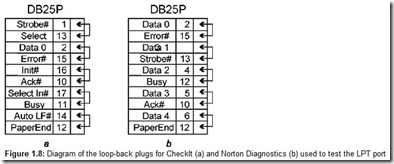
Troubleshooting ports with the help of diagnostic software allows you to inspect the output register. With the help of special plugs, the input lines can be checked, too. Because the number of port output (12) and input (5) lines is different, thorough port testing with a passive loop-back plug is not possible. Different diagnostic programs require different loop-back plugs (Fig. 1.8).
Most problems during work with the LPT port are caused by the connectors and cables. To check a port, a cable, or a printer, you may use special tests from some popular diagnostic programs (Checklt, PC Check, etc.). Alternatively, you simply can try to print an ASCII file.
-
If a file apparently can be printed from DOS (i.e., the file is copied on the device named LPTn or PRN quickly and without errors), but the printer has not issued a character, then there likely is a break (i.e., a bad contact in the connector) in the Strobe# circuit.
-
If the printer is online, but a message says it is not ready, the problem should be sought in the Busy line.
-
If the connection to the port printer works properly in the standard (SPP) mode, but starts malfunctioning when switched into the ECP mode, then the cable needs to be checked to ensure it meets the IEEE 1284 requirements. Cheap cables with untwisted wires usually work between 50 KBps and 100 KBps. However, between 1 MBps and 2MBps, available in the ECP mode, they may refuse to work, especially if the cable length exceeds 6.5 feet.
-
During the installation of a plug-and-play printer driver, you may receive a message that says a “bidirectional cable” is required. In this situation, check for a connection between DB-25 connector pin 17 and Centronics connector contact 36. Although this connection was stipulated originally, it is absent in some cables.
-
If the printer distorts the output, a break (or a short-circuit) in the data lines is possible. In this case, it will be handy to use a file that contains the code sequence of all printable characters. If certain characters or groups of characters are repeated when such a file is printed, the broken data-line wire can be easily determined by the period pattern of the repetition. It is practical to use the same file to check the hardware localization of the printer.
Hardware interrupts from the LPT port are not always used. Even the DOS background-printing program works with the port by status polling, and its servicing process is launched at the timer interrupt. Therefore, malfunctions of the port interrupt circuit rarely appear. However, a truly multitasking operating system (such as NetWare) attempts to work with the port via interrupts. The interrupt line can be tested only by connecting a peripheral device or a plug to the port. If a network adapter is connected to a port with an out-of-order interrupt channel, it probably will work—but at a low transfer rate. Any request will be answered with a delay of tens of seconds because the packet received from the adapter will be processed not at an interrupt (i.e., upon arrival), but at the external timeout.







![Table 1.11 Computer-Computer Connection Cable (4 bits wide)[1] Table 1.11 Computer-Computer Connection Cable (4 bits wide)[1]](http://machineryequipmentonline.com/electric-equipment/wp-content/uploads/2021/02/Table-1.11-Computer-Computer-Connection-Cable-4-bits-wide1_thumb.jpg)

