FABRICATION TECHNOLOGIES AND DESIGN ISSUES
This section identifies and discusses the underlying semiconductor technologies that are used to fabricate programmable-logic and ASIC devices. The design options, the design flow and synthesis technologies used for the PLASIC will be explained.
6.1.1 ASIC fabrication technologies
ASICs are normally fabricated using complementary metal oxide silicon (CMOS) technology. This subsection outlines the essential properties of CMOS devices, and shows how some of the basic circuit elements of an ASIC are implemented in CMOS. It first classifies the functional elements of an ASIC, and then gives an explanation of the ASIC fabrication process.
(1) Basic CMOS principles
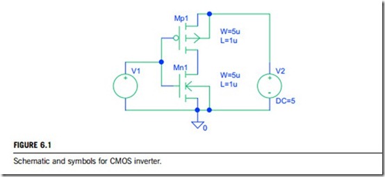
The metal oxide silicon (MOS) transistor is a field effect device. Two types of MOS transistor are used on ASICs; n-types and p-types. These are identical in structure but have opposite polarity charge carriers, hence the term complementary metal oxide silicon. Modern devices use polysilicon gates and not metal, but the name has remained the same. The point to note is that the field effect transistors are enhancement devices. They require their gate voltage to be a threshold voltage, above their source in the case of the n-transistor, and below source for the p-type transistor. An n-type and a p-type together (Figure 6.1) form the inverter which is the most basic primitive to be found in an ASIC library. P-type and n-type transistors are used in pairs for all CMOS devices.
(1) CMOS implementation of primitive parts
The use of symbols to represent schematics as in Figure 6.1 is important. A symbol at this level represents a part whose schematic is a transistor configuration. It is called a primitive part because it is at the lowest level of the parts hierarchy, and cannot be decomposed into simpler parts. Higher-level parts have schematics made up of symbols from lower-level parts, including primitive. ASIC manu- facturers supply a library of primitive parts represented as symbols. To some extent, designing with these symbols is rather like designing discrete logic from a data book of parts. This analogy should not be carried too far, because the principles of hierarchical ASIC design are not the same as those used when designing with discrete logic.
Another way of representing the characteristics of primitive parts is in terms of a switch-level model. The switch-level model of an inverter is another useful model up to quite high frequencies, typically above 20 MHz. It also helps in the understanding of such concepts as absolute and relative fan-out, drive strength and asymmetric drive capability.
A transistor can be configured into three gates: NAND, NOR, and ANDNOR Gates. In additional, comparators, decoders and inequality detectors form essential control elements in synchronous systems. They are related decoders perform a static, fixed comparison, whereas comparators perform a variable register-to-register comparison.
(2) Transmission gate and tristate buffer
Transmission gates represent a use of CMOS transistors that is not found in transistor-transistor-logic families. The transmission gate is an interesting primitive that is a true switch having two states; high impedance and low-impedance. However, great care must be taken to understand the nature and use of transmission gates, and how they can be transformed into triple state buffers.
(3) Edge-sensitive flip-flop
The edge-sensitive flip-flop is the basic storage element of a static, synchronous ASIC. Its essential property is that, on a rising clock edge, the logical state of input d is latched to output q, and that these output states persist until the next rising clock edge. A number of more complex latches, with feedback to retain data over successive clock cycles, and multiplexers to select the source of input data, are all derived from this basic cell. These form the basis of synchronous techniques for ASIC design.
(4) Classification of signals
All signals in a static synchronous ASIC can be classed as either clock, control or data.
1. The single clock signal is used to control all edge-sensitive latches, and for no other purpose. It is not gated with any other signal.
218 CHAPTER 6 Programmable logic and application specific integrated circuits (PLASIC)
2. Control signals, such as enable and reset, are used to initialize circuit elements, hold them in their current state, and make choices between input signals or route signals to alternative outputs. They may all originate from a single enable generator, controlled by the state counter.
3. Data signals carry data, as individual bits or in buses, around the ASIC.
(5) Classification of base primitives
The set of primitive parts which are used to build up the hierarchical structures in a static synchronous ASIC can be classified as follows:
1. Boolean primitives which include: Inverter, AND, OR, exclusive OR (non-equivalence), NAND, NOR, exclusive NOR (equivalence) ANDNOR, ORNAND.
2. Switch primitives which include: transmission gate, multiplexer and triple state buffer.
3. Storage primitives.
Edge-sensitive flip-flop can include:
1. Control elements: decoder, comparator, inequality detector.
2. Data conditioning elements: adder, multiplier, barrel shifter, and encoder.
(2) The ASIC fabrication process
Having prepared the functional elements of an ASIC, we are now at the position to look at the ASIC fabrication process.
Those ASICs that are made for CMOS are manufactured by a process of repeatedly etching a chemical resist layer on to a silicon wafer to a required pattern, and then chemically diffusing, growing or etching layers. The resist layer is formed either by a photolithographic process, or by electron beam exposure. In general, photolithography is quicker, but has the disadvantage that mask contamination is replicated across the wafer. Other disadvantages are that the maximum chip size is limited by the final aperture in the lithographic equipment.
Device geometry (the minimum polysilicon track width possible with the process), is often quoted
as a measure of the performance of a process. Small geometries, at present a 1.5 micron process, are faster than larger geometries such as 3 micron. Smaller geometries produce higher speeds due to lower gate capacitance, lower transition time across gates, and a higher packaging density which reduces track loading. Device geometry is only slightly dependent on whether the process is electric-beam or optical-beam in nature; the most variable component is the quality of the resist. As technology moves on, other limiting factors are likely to become more significant. The question of photolithography versus electric-beam is of more concern to accountants than to systems engineers, because it affects the unit price for various fabrication batch sizes.
During manufacture, process control monitors, or drop-ins are placed onto the wafer between customer designs. On a typical processor-control monitor there are raw transistors and via chains to test the parameters of the process for instances the threshold voltage. Some monitors for process control include RAM to test process yield, and a standard component such as a UART to test process performance at speed.
Approximately ten layers are required to create a working CMOS device. The top few layers are those of interest to the systems engineer; the two metal interconnect layers and the insulation layers (or via layers as they are known). The CMOS device can be regarded as a microscopic tray of transistors with their legs in the air, connected by a double-layer printed circuit board. Between the individual chips there are scribe channels to allow the wafer to be cut into individual chips.
After fabrication and while still in wafers, the chips are tested for fabrication faults by running a set of test vectors developed as a part of the ASIC design process. These are applied by test rigs through probes which contact the pads on the chip. The chips which pass the tests are packaged, and their pads bonded to the package pins. The tests are repeated through the pins to identify packaging faults.
The percentage of the chips that pass the test is the yield of the wafer. The economics of ASIC production are heavily dependent on this yield. The physical manufacturing process is fine-tuned to maximize it, and a significant proportion of the ASIC design cycle is devoted to making the circuit easy to test, and developing test vectors which will identify as many faults as possible before the chip is packaged and placed into a system. The issue of testing ASICs is dealt with in subsection 6.1.3.
The ASIC design options
This subsection introduces the range of options and styles that are available for integrated circuit design. Because this chapter focuses on the programmable-logic design styles, this subsection places programmable logic in context. Full-custom design is a basic ASIC design, but is not covered below as its meaning needs little further explanation.
(1) Standard-cell design
A standard cell is a group of transistor and interconnect structures which provides a Boolean logic function (e.g., AND, OR, XOR, XNOR, inverters) or a storage function (flip-flop or latch). The simplest cells are direct representations of the elemental NAND, NOR, and XOR Boolean functions, although cells of much greater complexity are commonly used (such as a 2-bit full-adder, or mused D- input flip-flop). The cell’s Boolean logic function is called its logical view; functional behavior is captured in the form of a truth table or Boolean algebra equation (for combinational logic), or a state transition table.
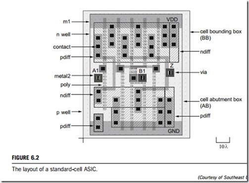
Figure 6.2 shows the layout of a standard cell. In reality, such a cell would be approximately 25 microns wide on an ASIC with l (lambda) ¼ 0.25 microns (a micron is 10 6 meter). Standard cells are stacked like bricks in a wall; the abutment box defines the “edges” of the brick. The difference between the bounding box and the abutment box is the area of overlap between the bricks. Power supplies (labeled VDD and GND in Figure 6.2) run horizontally inside a standard cell on a metal layer that lies above the transistor layers. Each shaded and labelled pattern represents a different layer. This standard cell has central connectors (the three squares, labelled A1, B1, and Z in Figure 6.2) that allow it to connect to others.
In the standard-cell design methodology, predefined logic and function blocks are made available to the designer in a standard-cell library. The standard-cell libraries of logical primitives are usually provided by the device manufacturer as part of their service. Usually their physical design will be predefined so they could be termed “hard macros”. Typical libraries begin with gate level primitives such as AND, OR, NAND, NOR, XOR, inverters, flip-flops, registers, and the like. Libraries then generally include more complex functions such as adders, multiplexers, decoders, ALU, shifters, and memory (RAM, ROM, FIFOs, etc.). In some cases, the standard-cell library may include complex functions such as multipliers, dividers, microcontrollers, microprocessors, and microprocessor support functions (parallel port, serial port, DMA controller, event timers, real-time clock, etc.).
Standard cell designs are created using schematic capture tools, or via synthesis from a hardware description language (HDL). Subsection 6.1.3 of this chapter will discuss the standard-cell design flow in more detail. Automated tools are then used to place the cells on a chip image and wire them together. Standard-cell designs operate at lower clock rates and are generally less area-efficient than a full custom design due to the fixed cell size constraints, and requirements for dedicated wiring channels. However, very high layout density is achieved within the cells themselves, resulting in densities which can approach that of full-custom designs, whilst needing substantially shorter design times.
(2) Gate-array design
Gate-array design is a manufacturing method in which the transistors and other active devices are predefined; and wafers containing such devices are held unconnected in stock prior to metallization. The physical design process then defines the interconnections of the final device. For most ASIC manufacturers, this consists of between two and five metal layers, each running parallel to the one below it. Non-recurring engineering costs are much lower, as photo-lithographic masks are required only for the metal layers, and production cycles are much shorter, as metallization is a comparatively quick process.
Pure, logic-only, gate-array design is rarely implemented by circuit designers today, having been replaced almost entirely by field-programmable devices, such as a field-programmable gate array (FPGA), which can be programmed by the user. Today gate arrays are evolving into structured ASICs that consist of a large ASIC IP core (ASIC IP means a semiconductor intellectual property) such as a CPU, DSP unit, peripherals, standard interfaces, integrated memories SRAM, and a block of reconfigurable uncommitted logic. This shift is largely because ASIC devices are capable of integrating such large blocks of system functionality, and because a “system on a chip” requires far more than just logic blocks.
In their frequent usage in the field, the terms “gate array” and “semi-custom” are synonymous. Process engineers more commonly use the term semi-custom, while gate array is more commonly used by logic (or gate-level) designers.
(3) Structured/platform design
Structured ASIC design (also referred to as platform ASIC design) is a relatively new term in the industry, which is why there is some variation in its definition. However, the basic premise of a structured/platform ASIC is that both manufacturing cycle time and design cycle time are reduced compared to cell-based ASIC, since the metal layers are predefined (thus reducing manufacturing time) and the silicon layer is pre-characterized (thus reducing design cycle time).
One other important aspect of structured/platform ASIC is that it allows IP that is common to certain applications or industry segments to be “built in”, rather than “designed in”. By building the IP directly into the architecture the designer can again save both time and money compared to designing IP into a cell-based ASIC.
(4) Field-programmable logic
A field-programmable-logic device is a chip whose final logic structure is directly configured by the end user. By eliminating the need to cycle through an IC production facility, both time to market and financial risk can be substantially reduced. The two major classes of field-programmable logic, programmable-logic devices (PLD) and FPGA, have emerged as cost-effective ASIC solutions because they provide low-cost prototypes with nearly instant “manufacturing”. This class of device consists of an array of uncommitted logic elements whose interconnect structure and/or logic structure can be personalized on-site according to the user’s specification.
The ASIC design flows
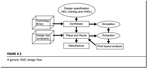
Nowadays, the design flow of ASIC has been highly automated. The automation tools provide reasonable performance and cost advantage over manual design processes. Broadly, ASIC design flow can be divided into the phases given below in this subsection, which are also illustrated in Figure 6.3.
Designing a programmable-logic or application-specific IC involves many different tasks, some carried out by the ASIC designers, while others are taken care of by the ASIC vendor. Since a digital ASIC cannot be changed once it is manufactured, verification of its functions is crucial before the masks for production are made. Therefore, considerable effort is needed to simulate the design at different levels to verify that no bugs exist. The ASIC design is described using a hardware description language, HDL. There are a number of such languages available, such as Verilog, VHDL, System C or System Verilog. The language can describe the hardware at different levels of detail. The most common level used today is called register transfer level, RTL. This level describes the functions of the ASIC with logic relations between memory elements (registers).
Simulation is a key step for the programmed functions to verify their correctness, but they also need to be translated into hardware, i.e. logic gates. This is called synthesis and is done using software tools. The result of the synthesis must be verified, both from a functional and a timing perspective. This is done by gate-level simulations, or by comparing the logic produced by synthesis to the programmed functions in the HDL. The latter is called formal verification or equivalence check. A floorplan/layout tool places the logic gates on a model of the physical ASIC. This enables the calculation of signal delays between all logic elements.
Due to an increase in signal speed, miniaturization of features, smaller chip sizes, and lower power supply voltages, interconnect signal integrity problems have increased. Signal delay due to inter- connect delay is more significant than gate delay. As a result, more powerful automation tools are required for layout parameter extraction, timing delay and crosstalk simulation, and power analysis. Static timing analysis (STA) is also used to constrain the layout tools and to verify that the design will work at the specified frequency. When the ASICs are manufactured, each chip needs to be tested in order to ensure that all delivered devices work properly.
The ASICs are tested using test vectors; either functional vectors or automatically generated vectors, or both. Functional vectors apply signals to the ASIC which are similar to the signals that the ASIC would receive in a real environment. Automatically generated vectors, on the other hand, only apply signals to verify that no defects exist within the ASIC, without relating to how the ASIC will be used in its target environment. This area of work is called design for test.
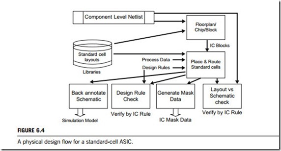
To gain better understanding of the ASIC design flow, design issues for the standard cell are taken as an example, and discussed in the following paragraphs. Usually, the initial design of a standard cell is developed at the transistor level, in the form a transistor netlist. This is a nodal description of transistors, of their connections to each other, and their terminals (ports) to the external environment. Designers use computer-aided design (CAD) programs to simulate the electronic behavior of the netlist, by declaring input stimulus (voltage or current waveforms) and then calculating the circuit’s time domain (analogue) response. The simulations verify whether the netlist implements the requested function, and predict other pertinent parameters such as power consumption or signal propagation delay. Figure 6.4 is a physical design flow for standard-cell ASIC.
Standard-cell ICs are designed in the following conceptual steps (or flow), although they overlap significantly in practice. These steps, implemented with the level of skill common in the industry, almost always produce a final device that correctly implements the original design, unless flaws are later introduced by the physical fabrication process.
1. The design engineers start with a non-formal understanding of the required functions for a new ASIC, usually based on a customer requirements analysis.
2. The design engineers construct a specification of an ASIC to achieve these goals using an HDL. This is usually called the RTL (register transfer level) design.
3. Suitability for purpose is verified by functional verification. This may include such techniques as
logic simulation, formal verification, emulation, or creating an equivalent pure software model.
4. Logic synthesis transforms the RTL design into a large collection of lower-level constructs called standard cells. These constructs are taken from a standard-cell library consisting of precharacterized collections of gates. The standard cells are typically specific to the intended manufacturer of the ASIC. The resulting collection of standard cells, plus the necessary electrical connections between them, is called a gate-level netlist.
5. The gate-level netlist is next processed by a placement tool which places the standard cells onto a region representing the final ASIC. It attempts to find a placement of the standard cells, subject to a variety of specified constraints.
6. The routing tool takes the physical placement of the standard cells and uses the netlist to create the
electrical connections between them. The output is a file which can be used to create a set of photo- masks enabling a semiconductor fabrication facility to produce physical ICs.
7. Given the final layout, circuit extraction computes the parasitic resistances and capacitances. In the case of a digital circuit, this will then be further mapped into delay information, from which the circuit performance can be estimated, usually by static timing analysis. This and other final tests, such as design rule checking and power analysis (collectively called signoff), are intended to ensure that the device will function correctly over all extremes of the process, voltage and temperature. When this testing is complete the photo-mask information is released for chip fabrication.
These design steps (or flow) are also common to standard product design. The significant difference is that the latter uses the manufacturer’s cell libraries that have been used in potentially hundreds of other design implementations, and therefore are of much lower risk than full custom design. Standard cells produce a cost-effective, design density and they can also integrate IP cores and SRAM (static random access memory) effectively, unlike gate arrays.


