S-correction
Recall that in order to compensate for the flat surface of the tube face, correction of the line scan waveform is necessary. This correction, known as symmetrical or S-correction, becomes increasingly important with wide- angle deflection tubes.
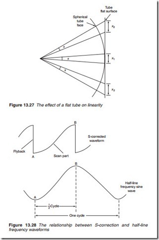
As can be seen from Figure 13.27, an equal angular deflection of the beam scans a smaller distance at the centre compared with the distance it scans at the two ends of the line. Thus, to obtain a linear picture scan using a flat tube face, a non-linear angular deflection is necessary. The purpose of the non-linearity is to slow the rate of change of the angular deflection at both ends of the scan (Figure 13.28). Since the current through the line scan coils is responsible for the angular deflection, the corrected waveform must be of the same shape.
The scan part of the S-correction waveform approximates a half-cycle of the half-line frequency sine wave in Figure 13.28. The scan part may be simply obtained by connecting a tuning capacitor in series with the scan coils. The value of the capacitor is chosen so that it resonates with the scan coils at a frequency slightly higher than half the line frequency, approxi- mately 7.8 kHz. This provides time duration from A to B of
In the line output stage of Figure 13.29, C2 is the S-correction capacitor which has a value of between 1.5 and 3 j.LF. The scan coils are transformer- coupled to the line output transistor TR1. D1 is the efficiency diode and C1 is the flyback tuning capacitor.
Modern TV receivers employ direct coupling (Figure 13.30). At the end of the scan, TR1 is switched off, tuned circuit L1/C1/C2 is pulsed into oscillation to provide the flyback AB. At the negative peak (point B), diode D1 conducts placing C2 across L1 to commence an oscillation at a fre- quency of
The first half-cycle of this oscillation, BC, provides the scan. At approximately one third of the scan, TR1 is switched on and takes over from the diode, and so on.
Further simplification of the line timebase circuit may be obtained by using the b–c junction of the output transistor TR1 as the efficiency diode (Figure 13.31). The polarity of the b–c junction is the same as the polar- ity of an efficiency diode, had it been connected; the n-region collector (cathode) is connected to h.t. whereas the p-region base (anode) is con- nected to chassis via the secondary winding of T1. At the end of the scan, the b–c junction is forward biased in the same manner as an efficiency diode.

