DTV RECEIVER
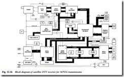
A simplified block diagram of a DTV receiver is shown in Fig. 12.16. This one is for satellite reception, so the four main blocks at the top are customised for QPSK operation.
Channel decoder
The two primary functions of the channel decoder section are to lock onto the main (home) channel, and to detect the broadcast data- stream, correcting it as necessary. The tuner has two oscillators, one under the control of the FS tuning system (see Chapter 3) and the second under the control of the QPSK demodulator chip, to separate I (in-phase) and Q (quadrature) carrier components. They go on to the ADC chip where sampling takes place, paced by a clock in the QPSK chip. The resulting two streams of 6-bit data pass into the QPSK demodulator IC which produces two 3-bit datastreams for application to the FEC decoder. This FEC chip can detect errors in both the symbols and the packet bytes, and correct them in many cases; those which are damaged beyond repair are deleted to prevent them causing mischief further downstream. Eight-bit data emerges from the FEC chip as MPEG data.
Control of the channel decoder by the microcontroller chip is primarily via two bus systems: the familiar I2C serial type for tuner and other control; and an 8-bit parallel bus conveying address information and data to and from the QPSK and FEC chips. In addi- tion to these there are two important feedback signals from the FEC section to the microcontroller, MPEG FAIL and DVALID OUT, the first to indicate seriously corrupt data, and the second to signify that the channel decoder has lost synchronisation. With both of these at 0 V, the microcontroller puts up a ‘no-signal’ indication, resets the tuning to a default channel (stored in memory) and initiates a tun- ing scan. The process continues until another DTV transmission is found and the channel decoder locks up once more.
Transport demultiplex
We left the outputs from the channel decoder as an 8-bit parallel MPEG data feed. They enter the transport demux chip with three control signals: MPEG FAIL, to flag erroneous packets; MPEG START, a timing mark for the start point of each data packet; and MPEG CLK, the data-rate clock. Using the PID data and the details of the programme requested by the user, the demux chip extracts all the relevant data packets, sending them to the Conditional Access (CA) module for decryption. ‘Clear’ programmes can be dealt with in the transport section without reference to the CA module. The required packets are assembled within the SRAM near the middle of the diagram so that complete blocks of video data can be sent at intervals to the MPEG video decoder – each time the SRAM fills up. Similarly, the MPEG audio decoder is fed by ‘bursts’ of audio data, converted from parallel to serial form inside the transport demux chip.
Two further functions of the transport demux IC are to extract from the datastream a clock-sample code and produce from it a synchronised 27 MHz reference clock by means of a PLL; and (in this particular receiver design) to relay operating instructions from the control microprocessor to the video decoder.
MPEG video decoder
The decoder is the heart of the DTV receiver, in which the picture is reconstructed from the I, P and B frames described earlier. Picture data enters the MPEG video chip on an 8-bit data bus, directed by a 6-bit address code from the transport section. The picture data is expanded within the DRAM (bottom LHS of Fig. 12.16) back to complete values of Y, Cb and Cr for each pixel in each TV frame for the reconstituted picture. Data traffic to and from the DRAM is via a 64-bit parallel data bus, with addressing information on a 9-bit bus. Further address data is conveyed in row and column address strobe lines, while read and write processes are controlled by OE and WE memory control lines. The memory processing is timed and synchronised by a dedicated 55 MHz clock, while the 27 MHz system clock governs the decoding process and sync pulse generation and timing.
Y, Cb and Cr data passes out of the MPEG decoder chip on an 8-bit bus to a combined D−A converter and PAL encoder, which produces a standard PAL video signal, an S-VHS (Y/C) variant, and RGB outputs for direct coupling to a monitor or suitably equipped
TV set. This design also has an RF modulator for full versatility in coupling the receiver to other equipment.
MPEG audio reception
Compressed MUSICAM audio data in serial form is passed from the transport demux chip to the MPEG audio processor in time with a data strobe signal AUD DSTR. Within the audio chip the sound data is expanded and reconstituted, then stored for up to one second in the audio DRAM (RHS of Fig. 12.16) to achieve synchronisation with the video signal; the delay time is governed by the time-stamps sent with the broadcast data. Also in the broadcast data is a code describing the sampling frequency used in the audio encoder: 48, 44.1 or 32 kHz. It is regenerated by a programmable clock generator for use within the decoder and D−A converter (bottom RH corner of the diagram) sections. The data passes between the two latter as a serial PCM datastream, and the conversion process is governed by three pulse trains: sample clock, L/R clock and PCM clock.
Decoder control
The operation of both MPEG decoders, video and audio, is governed entirely by the 16-bit 68306 microprocessor chip, whose operating program is held in the flash memory chip. This type of memory store can be upgraded by broadcast data as necessary. New program upgrades are initially deposited in the DRAM memory by the microprocessor, then transferred to the flash chip in complete data blocks, reading and verifying each as it goes. The flash memory is non-volatile, and is addressed and interrogated at each switch-on of the receiver.
The audio decoder is governed by the microprocessor via an interface called a PLD (Programmable Logic Device) which also provides control data for the CA module. Communication is effected by an 8-bit data bus and a 7-bit address bus.
Conditional Access
Service information sent by the programme provider indicates to the microprocessor which programmes are encrypted. When an encrypted programme is requested by the viewer the processor brings the Conditional Access Module (CAM) into operation. Communica- tion between the two is by an 8-bit data bus and a 13-bit address bus, plus six additional lines for data/address strobing, read/write, chip select, acknowledge and reset purposes. Within the CAM is an IC
(ICAM) designed to decrypt both audio and video packets in conjunction with the data held in the viewer’s smart card, for which a subscription is payable. So long as the card is valid for the programme, the ICAM decrypts the packets using a buffer memory (DRAM) chip, and passes them back out to the transport demux chip on an 8-bit bus.
Receiver control
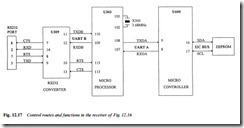
The 68306 microprocessor is primarily concerned with governing the decoding processes, though it takes complete control of the receiver at switch-on, during data transfer via the RS232 port, and when flash- memory reprogramming data is being received. All the normal ‘housekeeping’ functions of the sorts described in Chapter 22 are undertaken by the NEC microcontroller. An idea of the interconnections between the main control sections of the DTV receiver is given in Fig. 12.17.
Modem
Although not shown in Fig. 12.16, the receiver incorporates a modem for use with Pay Per View (PPV), home shopping programmes and ‘interactive’ systems. Similar in nature to the type used with computers, it can dial advertiser’s and programmerovider’s numbers on the public telephone network. PPV information can be sent to the programme provider in one of three ways. The card may be programmed to send the data at a specific date and time, e.g. at the end of each month. Here the command would be read by the CA section and actioned at the right time by the control processor. Alternatively the card can be given a predetermined credit limit: when it is reached the CA section initiates (via the main processor) a call to the broadcaster. The third method is for the service provider to request the PPV information by transmitting a command signal, which can include a telephone number.

