Switched-mode power supplies
In the low and medium power range, 50 W and over, a regulated d.c. source is often required which contains negligible a.c. ripple. For these application, the switched-mode power supply (SMPS) is often used. Apart from reducing a.c. ripple, switched mode power supplies are more effi- cient than the linear types, dissipating less heat and are smaller in size. The SMPS is basically a d.c.-to-d.c. converter; it converts d.c. into a switched or pulsating d.c. and back again into a d.c. The switching speed determines the a.c. content or ripple frequency at the output.
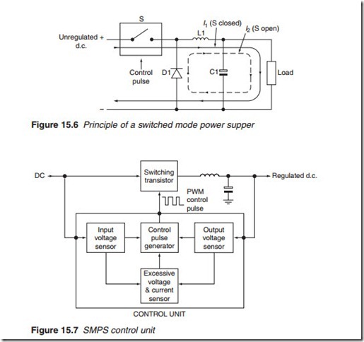
The basic principle of a switched mode power supply circuit is shown in Figure 15.6. When the switching element S is closed, current I1 flows from the positive side of the unregulated input into the load as shown. The magnetic field set up by the current flowing through L1 causes energy to be stored in the inductor. When the switch is open, the current ceases and the magnetic field collapses. A back e.m.f. is induced across the inductor in
such a way as to forward-bias D1, causing a current I2 to flow into the load in the same direction as I1. The energy stored in the inductor when the switch was closed is transferred to the load to keep the load current con- stant. The ripple at the output has a frequency that is twice the switching speed and is easily removed by the low-pass filter action of L1/C1.
The switching element may be a bipolar power transistor or a power MOSFET; opened and closed at regular intervals by a pulse from a control unit. Regulation is obtained by making the time intervals when the switch- ing element is open and closed (i.e. the mark-to-space ratio of the control pulse) depending on the d.c. output. They may also be made to depend on the input voltage; this guards against changes in the mains (or battery) sup- ply voltage as shown in Figure 15.7. The control unit, which is normally an IC package, may also provide protection against excessive current and volt- age. The control pulse is in essence a pulse-width modulated waveform
(PWM) obtained from a free-running oscillator or an oscillator driven by line sync pulses.
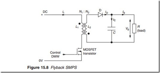
There are three main types of switched mode power supplies: Flyback or Boost, Forward or Buck and Cuk converters. A flyback-type SMPS is shown Figure 15.8 employing an isolating transformer. Apart from the isolation between ‘hot’ and ‘cold’ sides, the transformer also provides a simple way of obtaining a range of d.c. outputs by simply employing a number of secondary windings with different turn ratios.
The transformer windings are such that the voltage and current in the secondary L2 are in anti-phase to their counter part in the primary as denoted by the dots. When the MOSFET transistor is turned on, current flows into the primary of the transformer causing a current to flow in the secondary winding L2 in the opposite direction. Diode D is reverse biased and energy is stored in inductor L2. When the MOSFET switches off, inductor current ceases and the back e.m.f. across L2 forward biases the diode and energy is transferred from L2 to capacitor C and hence to the load. The process is then repeated when the transistor is switched on again and so on.
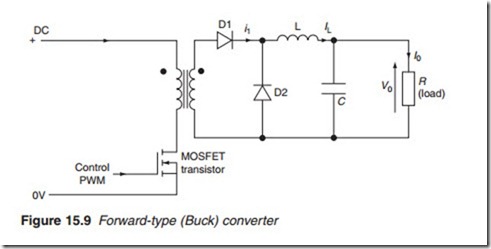
A forward-type (Buck) converter is shown in Figure 15.9. When the MOSFET is turned on, the induced secondary voltage turns diode D1 on and energy is stored in inductor L. When the transistor is turned off, inductor current collapses and a back e.m.f. appears across it. D1 is reverse biased and D2 is forward biased. Energy is transferred from the inductor to the capacitor which charges up to keep a stable voltage across the load. L/C also acts as a low-pass filter.
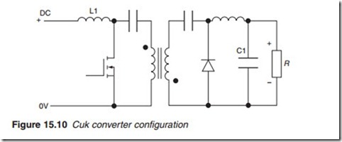
A Cuk converter configuration is shown in Figure 15.10. The operation of the Cuk is slightly more complex than the other two types, but essen- tially, when the MOSFET is on, current flows in the inductor and energy is stored in L1. When the transistor turns off, energy is transferred from the inductor to capacitor C1 via the transformer windings.
A typical flyback converter for a TV receiver, commonly known as a chopper power supply is shown in Figure 15.11. Electrical isolation between live mains and the circuits of the TV is provided by the (chopper) trans- former whose primary and secondary windings are separated by insulat- ing layers capable of withstanding over 2 kV. To maintain mains isolation, an isolating break in the feedback path is necessary. This may be provided by a transformer, but normally an opto-coupler is used as shown. The opto-coupler consists of two highly insulated halves, linked by an infrared light beam, generated by a light-emitting diode (LED) and monitored by a photo-transistor. An increase in the diode current and hence its emit- ted light would cause the photo-transistor current to go up as well. The isolating transformer makes it possible to obtain a number of regulated d.c. rails by merely adding secondary windings. The ‘chopper’ transistor TR1 is normally a bipolar or a MOSFET transistor. Network D3/R1/C1 provides protection for the chopper transistor against excessive rise of col- lector voltage caused by the turns off. When TR1 is off, its collector volt- age rises, turning D3 on. This effectively places snubbing capacitor C1 across TR1, diverting the major part of the back e.m.f. energy away from


