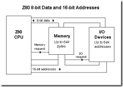
ILLUSTRATIVE EXAMPLE 1: INTERFACING 2764 EPROM

In this section, we will illustrate memory interfacing with the Z80 microprocessor by using an actual chip: the 2764 PROM (Erasable Programmable Read-Only- memory). This is a memory chip commonly used in industry to develop microprocessor-based products .. In this illustration, we will assume that the chip bas been already programmed-that is the binary patterns representing Z80 instructions are stored in it-and we will only read from it , we focus only on the interfacing concepts, Interfacing logic circuit, and memory addresses.

2764 EPROM

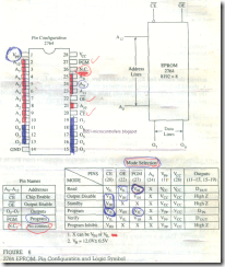
This is an 8K (8192 x 8) memory chip with eight data lines and is housed in a 28-pin package : Figure 6 shows the logic pinout and the pin configuration. It has thirteen address lines, A12-A0 to identify 8192 registers one chip select signal shown as chip enable (C͞E) and one output Enable (O͞E) signal to enable the output buffer.

microproccessor-architecture&memory-interfacing-34_03

FIGURE 6

2764 EPROM: Pin Configuration and Logic Symbol

It operates from a single + 5 V power supply in the Read mode and requires +21 V pulse Vpp to program It . the pinout of this memory chip is compatible with 27128 ( 16K x 8) and 2256 (32K x 8) EPROMs; thus, the memory size can be expanded to 16K or 32K by merely replacing the chip. The chip has a quartz window, and the information stored in this memory can be erased by ex posing the window to ultraviolet light for 15 to 20 minutes. The erasing process sets all the bits to logic 1. To avoid accidental erasures from direct sunlight or fluorescent lights, the window should be covered with an opaque label. Once it is erased, the chip can be used again to store a new program. The programming is done by using a circuit called an EPROM programmer that can selectively store logic 0 in bit positions In memory registers by providing a 21 V pulse to Vpp

Interfacing Circuit

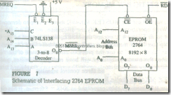
Figure 7 shows a complete schematic of interfacing the 2764 with the Z80 mi­croprocessor. We will describe this circuit in terms of the four steps required for interfacing, as listed in the previous section.

Step 1 : Connect the necessary address lines to the memory chip.

Figure 7 shows that the address lines A12-A0 are connected to the memory

chip to identify 8192 registers.

Step 2 Decode the remaining address lines and combine the M͞R͞E͞Q with the & decoded pulse to generate the Memory Select (M͞S͞E͞L) pulse.

Step 3:

In this schematic, two steps-the decoding of the address and generating the Memory Select (M͞S͞E͞L)-are combined by using the 74LS138 3-to-8 decoder. The decoder has three inputs, three enable lines, and eight output lines. Two enable lines are active low, and one is active high. Once the decoder is enabled, only one output line, corresponding to the input, combination, goes active (low).

microproccessor-architecture&memory-interfacing-5_03

FIGURE 7

Schematic of Interfacing 2764 EPROM

In Figure 7, the output O0 of the decoder is shown as Memory Select (M͞S͞E͞L0), which is connected to the Chip Enable (C͞E) of the memory, and O0 goes active low when the address lines A15– A13 the M͞R͞E͞Q are all at logic 0 . The control signal M͞R͞E͞Q is used to enable the decoder (active low); the address lines A15, A14, and A13 are used as input to the decoder; the enable line E3 is connected to + 5 V; and E2 is grounded. No other logic level on these address lines can assert the M͞S͞EL0 signal.

Step 4: Connect the Z80 control signal to enable an appropriate buffer.

Figure 7 shows that the Z80 Read (R͞D) is connected to the R͞D signal of the memory chip. When the R͞D signal is asserted, the output buffer is enabled and the data byte from the selected register is placed on the data bus.

Memory Map

We can obtain the address range of this memory chip by analyzing the possible logic levels on the 16 address lines. The logic levels on the address lines A15-AI3 have to be 0 to assert the Chip Enable, and the address lines A12-A0 can assume any combinations from all 0s to all 1s. Therefore, the memory map (the address range) of this chip is from 0000H to 1FFFH as shown below.

microproccessor-architecture&memory-interfacing-36_03

We can verify the memory map in terms of our analogy of page and line numbers. The chip has 8192 bytes of memory that can be viewed as 32 pages with 256 lines each. Let us examine the high-order Hex digits of the map; they range from 00 to 1F indicating 32 pages-0000 to 00FF, 0100 to 01FF, for example.


How does the Z80 Read from or Write into Memory?

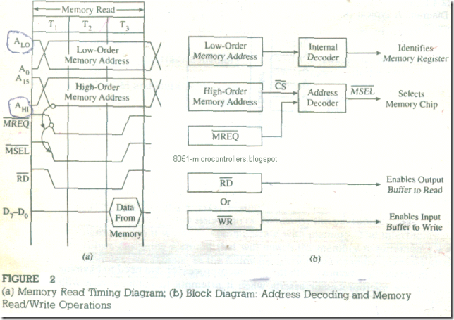
In Topic 3, we showed t e timing diagrams and the Z80 bus contents When an opcode or a data byte is fetched from memory. To read from memory, the Z80 performs the following steps, as shown in Figure 2(a) :

1- Places a 16-bit address on its address bus (shown as high- and low order addresses )

2- Asserts the M͞R͞E͞Q to indicate that the address bus holds a valid address

3- Asserts the R͞D signal low to indicate that it wants to read .

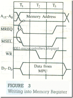
To write into memory, the Z80 performs the following steps, as shown in Figure 3:

1- Places a 16-bit address on its address bus

2- Asserts M͞R͞E͞Q and places data on the data bus .

3- Asserts W͞R signal

To understand and design an interface circuit, we need to match the memory requirements with the Z80 read/write operations.

microproccessor-architecture&memory-interfacing-30_03

FIGURE 4.2

(a) Memory Read Timing Diagram; (b) Block Diagram: Address Decoding and Memory Read/Write Operations

Basic Concepts in Memory Interfacing

The primary function of memory interfacing is to allow the microprocessor to read from and write into a given register of a memory chip To perform these opera­tions, the microprocessor should

  1. be able to select the chip.
  2. Identify t the register

3. Enable the appropriate buffer.

Let us examine the timing diagram of the memory read operation – figure 2(a) – in order to understand how the Z80 can read from memory in figure 2(a) the address bus is divided into two segments low order A0-AI.O and high order AH1-A15 to explain the decoding concepts the number of address lines represented by the ALO and AH1 varies according to the size of the memory chip .

The Z80 places a 16-bit address on the address bus and with this address only one register should be selected for the memory chip in figure 1 only ten address lines are required to identify 1.024 registers therefore we can connect the low-order address lines A9-A0 (ALO = A9 ) of the Z80 address bus to the memory chip.

microproccessor-architecture&memory-interfacing-31_03

FIGURE 3

Writing into Memory Register

The internal decoder of the memory chip will identify and select the register, as shown in Figure 2(b) .

2. The remaining Z80 address lines A15-A10 (AH1 = A10) should be decoded to generate a Chip-Select (C͞S) signal unique to that combination of address logic .

3. The Z80 provides two signals: M͞R͞E͞Q and R͞D. The M͞R͞E͞Q can be combined with decoded address pulse (C͞S) to generate a Memory Select (M͞S͞E͞L) to select the memory chip .

4. The microprocessor asserts the control signal R͞D, enables the output buffer of memory, and reads the data byte. Figure 2(a) also shows that memory must place the data byte on the data bus at the beginning of T3 .

To write into a register, the microprocessor performs similar steps. Figure 3 shows the Memory Write cycle. In the Write operation, the Z80 places the address and data, and asserts the M͞R͞E͞Q signal. After allowing sufficient time for data to become stable it asserts the Write (W͞R) signal, The W͞R signal enables the input buffer of the memory chip-and store the byte in the selected register.

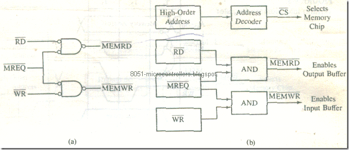
An alternative to generating the M͞S͞E͞L signal (Step 3 in Memory Read) to select the memory chip is generate the control signals M͞E͞M͞R͞D and M͞E͞M͞W͞R by-combining the M͞R͞E͞Q , R͞D, and W͞R as shown in Figure 4). The M͞E͞M͞R͞D can be used to enable the output buffer to read from memory; the M͞E͞M͞W͞R can be used to enable the input buffer to Write into memory, and the decoded address pulse (C͞S) can be used to select the chip as shown in Figure 4(b).

To interface memory with the microprocessor, we can summarize the above steps as follows:

1. Connect the required address lines of the address bus to the address lines of the memory chip.

2. Decode the remaining address lines of the address bus to generate the Chip

Select signal, as discussed in the next section (4).

microproccessor-architecture&memory-interfacing-32_03

FIGURE 4

(a) Generating Control Signals; (b) Block Diagram: Alternative Approach to Memory Read/Write Operations

3. Generate the signal Memory Select (M͞S͞E͞L) by combining the decoded address pulse C͞S and the M͞R͞E͞Q , and the MSEL to select the memory chip .

4. Connect the Z80 R͞D and W͞R control signals to the R͞D and WR memory signals to enable memory buffers.

5 .An alternative procedure is to generate control signals M͞E͞M͞R͞D and M͞E͞M͞W͞R by combining R͞D and W͞R signals with the M͞R͞E͞Q and to use them to enable appropriate buffers. The decoded address pulse (C͞S) is used to select the memory chip.

Address Decoding

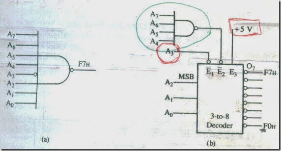
The process of address decoding should result in identifying a register with a given address ; we should be able to generate a unique pulse for that address for example in figure 5(a) the output of the NAND gate goes low (active) only when the address on the address lines is F7H no other address can cause the output of the gate to go low this process is called decoding the address we can also use a decoder for address decoding as discussed bolo war a PROM (programmable Read only memory ) as discussed in topic 16 .

Figure 5(b) shows a 3-to-8 decoder and a 4-input NAND gate the decoder has three enable lines one active high and two active low the enable line E1 is connected to address lines A2,A1, and A0 are inputs to the decoder, and the enable line E3 is tied high and is not being used here for decoding .

In this decoder circuit three input lines can have eight different logic combinations from 000 ot 111; each input combination can be identified by the corresponding output line if enable lines are active for example if the input is 0 0 0, O0 goes low (others remain high) and if the input is 1 1 0, O6 goes low , to Activate the enable line E͞1 , A3 should be low , and to activate E͞2 , address lines A7 – A4 should be high , causing the output of the NAND gate to go low , if the input to the decoder is 1 1 1 , the output line O7 of the decoder will go low , thus decoding the address F7H .

microproccessor-architecture&memory-interfacing-45_03g45

microproccessor-architecture&memory-interfacing-33_07

FIGURE 5 . Address Decoding

This 3-to-8 decoder can identify or decode eight addresses from FOH to F7H as shown in Figure 5(b). We will use this address decoding scheme, for interfac­ing memory chips in the following illustrations (Sections 2 and 3).


Introduction to Memory Interfacing

Memory is an integral part of a microprocessor ­based system, and in this topic our focus will be on how to interface a memory chip with the microprocessor. We will examine memory structure and requirements to read from it an write into it, We then compare those require­ments with those of the Z80 Memory Read and Write machine cycles, From that comparison, we will derive the basic steps necessary to in­terface memory.

This topic illustrates two .examples of interfacing memory chips, one EPROM and the other static R/W memory. The discussion in­cludes analyses of the following: decoding cir­cuits, memory maps, the concepts of fold back memory and absolute decoding. Finally, an example of memory design is illustrated to synthesize the interfacing concepts.

OBJECTIVES

  • List the requirements to read from memory.
  • List the steps initiated by the Z80 to read from and write into memory.
  • List the steps required to interface a memory chip with the Z80.
  • Analyze given EPROM and static R/W memory interfacing circuits and specify their memory address ranges.
  • Explain the terms absolute decoding and foldback memory.
  • Design a circuit to interface EPROM and R/W memory with the Z80 for given memory addresses.

INTERFACING MEMORY

While executing a program , the microprocessor needs to access memory fre­quently to read instruction codes and data stored in memory and the interfacing circuit enables that access. Memory has certain signal, requirements for writing into and reading from its registers. Similarly the microprocessor initiate a set of signals when it wants to communicate with memory . the interfacing process in­volves designing a circuit that will match the memory requirements with the mi­croprocessor signals. In the following section, we examine memory structure and its requirements and also the Z80 Memory Read and Write machine cycles. Then we derive the basic steps necessary to interface memory with the Z80 .

Memory Structure and Its Requirements

Read/Write Memory (R/WM) is a group of registers to store binary information.

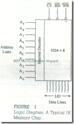
Figure 1 shows a typical R/W memory chip; it has 1024 registers, each of which can store eight bits indicated by eight I/O lines. the chip has ten address lines A9– A0 , one Chip Select C͞S, and two control lines : Read (R͞D) to enable the Output buffer and Write (W͞R) to enable the input buffer. Figure 4 also shows the internal decoder to decode the address lines. We may recall from Topic2 that to read from or write into one of the memory registers certain requirements have to

be met. They are as follows:

1- An address should be placed on the address lines the low-order address lines are decoded by the internal decoder of the memory chip , and the addressed register is identified .

2- The high order address should be decoded to generate a chip select signal and the memory chip is selected by asserting the chip select C͞S low .

3- To read from the addressed register the R͞D should be asserted low to enable the output buffer and then the data byte from the register will be placed on the I/O lines .

4- To write into the addressed register the W͞R should be asserted low to enable the input buffer and then data bits from the data lines are stored into the register .

microproccessor-architecture&memory-interfacing-29_03

FIGURE 1

Logic Diagram: A Typical 1 K Memory Chip,

To interface this memory with the Z80 microprocessor, we need to examine the signals the microprocessor asserts when it attempts to communicate with Memory


ASSIGNNIENTS on microprocessor architecture

1- The MOS Technology 6501 microprocessor chip has 13 address lines. Spec­ify the memory registers it is capable of addressing.

2- If the Intel 8086 microprocessor has 20 address lines, what is its capacity of memory addressing?

3- Explain the functions of the accumulator.

4- List the Z80 programmable registers.

5- What is a flag?

6- What is the function of the program counter?

7- If the Z80 is executing the code fetched from the memory location 1845H, what is the memory address in the program counter?

8- If the clock frequency is 4 MHz, how much time is required to execute an instruction of 21 T-states?

9- The instruction LD IX, (2050H) loads 2050H into the index register. Specify the number of bytes. machine cycles, and T-states of this instruction by checking the instruction set. Calculate the time required to execute the in­struction if the system clock frequency is 6 MHz.

10- List the sequence of events that occurs when the Z80 reads from memory.

11- In the Opcode Fetch cycle, what are the control signals required to enable the memory buffer?

12- When is the data byte placed on the data bus in the Memory Write cycle?

13- The memory location 2065H holds the opcode F9H , If the Z80 begins the Op­code Fetch cycle by placing the address 2065H on the address bus, specify the contents of the data bus after the falling edge of the T2 state.

14- The instruction LD B, (HL) copies the contents of the memory location specified by the 16-bit contents in the Hl, register. It is a l-byte instruction with two machine cycles. Identify the second machine cycle and its control signals.

15- In Figure 7(b), exchange R͞D and W͞R signals and identify the output pins and the control signals that can be generated at the output.

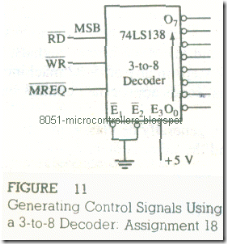
16- Figure 11 shows a 3-to-8 decoder with M͞R͞E͞Q. R͞D, and W͞R as input sig­nals. Identify the control signals that can be generated at the outputs of the decoder.

microproccessor-architecture&memory-interfacing-24_03

FIGURE 11

Generating Control Signals Using a 3-to-8 Decoder: Assignment 18

microproccessor-architecture&memory-interfacing-45_0345

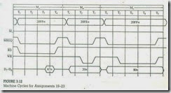
FIGURE 12

Machine Cycles for Assignments 19-23

17- Figure 12 shows the timings of three machine cycles. Identify the types of operations.

18- Do the three machine cycles in Figure 12 represent a complete instruc­tion? Explain.

19- Examine the machine cycle M, in Figure 12 and specify the memory being accessed and its contents.

20- Does the byte on the data bus in the machine cycle Mil in Figure 12 repre­sent an opcode?

microproccessor-architecture&memory-interfacing-25_06

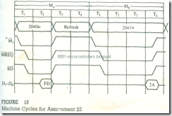
FIGURE 13

21- Explain what is being done in machine cycle Mc (Figure 12).

22- Identify the machine cycles Ma and Mb in Figure 13.

23- Identify the machine cycles in the following instructions:

SUB B : 1 By tell Machine Cycle/4 T-states

: Subtract the contents of register B from the accumulator

AND 47H : 2 B/2 MC/(4, 3) T-states

: Logically AND 47H with the contents of the accumulator

LD A, (2050H) : 3 B/4 MC/13 (4, 3, 3, 3) T-states

: copy the contents of the memory location 2050H into the accumulator

PUSH BC : 1 B/3 MC/10 (4, 3, 3) T-states

: copy the contents of BC register into two stack memory locations

Machine Cycles for Assignment 22


SUMMARY of microprocessor architecture

microproccessor-architecture&memory-interfacing-4545455454_03

· The Z80 signals can be classified into six groups: address bus, data bus, con­trol signals, external requests, request acknowledge, and power and frequency signals (see section 1 for definitions of these signals).

· The Z80 address bus has 16 unidirectional address lines; they are capable of addressing 64K memory.

· The Z80 data bus has eight bidirectional data lines, and they are used for data transfer.

· The Z80 microprocessor has six general-purpose 8-bit registers IB, C. D. E, H, and L) as a primary set. In addition, it includes the alternate set of these registers that can be used to exchange information with the primary set. The registers Band C, D and E, and Hand L can be combined to perform Some 16-bit operations.

· The ALU section of the Z80 includes accumulator A and the flag register to indicate six different data conditions. It also includes the alternate accumula­tor A’ and the flag register F’, which can be used to exchange information with A and F, respectively.

· Four flags-Sign, Zero, Carry, and Parity/Overflow-can be used for decision making and tested in conjunction with Jump, Call, and Return instructions. Two flags-Half Carry and Add/Subtract-are used internally for BCD opera­tions and are unavailable for the programmer.

· The Z80 has four 16-bit registers-IX, IY, Sp, and PC-used as memory pointers. Two index registers IX and IY are used to point to any memory lo­cation. The stack pointer (SP) is used to specify memory locations in a de­fined R/W memory segment called the stack. The program counter (PC) is used to sequence the program execution; it points to the next memory ad­dress from where the machine code is to be fetched.

· The Z80 is designed to execute 158 instruction types, and each instruction can be divided into a few basic operations called machine cycles.

· The frequently used machine cycles are Opcode Fetch, Memory Read and Write. and I/O Read and Write.

· The Opcode Fetch and Memory Read are operationally similar; the Z80 reads from memory in both machine cycles. However, the Z80 reads opcode during the Opcode Fetch cycle, and it reads 8-bit data during the Memory Read -cycle. In the Memory Write cycle, the Z80 writes data into memory.

· The memory operations are differentiated from I/O operations by two control signals: M͞R͞E͞Q and I͞O͞R͞Q. The signal M͞R͞E͞Q is combined with R͞D and W͞R signals to generate M͞E͞M͞R͞D and M͞E͞M͞W͞R control signals.

· The Z80 performs three basic steps in any of these machine cycles: It places an address on the address bus, sends appropriate control signals, and trans­fers data via the data bus.

· The 8-bit microprocessors can generally be classified into two categories: One group is register-oriented, and the other is memory-reference-oriented.


ARCHITECTURE OF SIMILAR 8-BIT MICROPROCESSORS

The primary reasons to discuss other 8-bit microprocessors are to examine how the MPU model developed in the last topic matches with various microproces­sors and to confirm that the underlying basic concepts remain similar even though specific details may vary from one chip to another. At present. many 8-bit general-­purpose microprocessors are available in the market. We will focus on three: the Intel 8085. the National Semiconductor NSC 800, and the Motorola 6800. These microprocessors are selected to illustrate various strategies used in designing the microprocessor. The recent trend in 8-bit microprocessors can be illustrated by so-called 8-bit super chips, such as the Hitachi HD64180, discussed in Topic 18.

Inte18085

The intel 8085 and its predecessor the 8080 are widely used 8-bit microprocessors. The 8080 MPU is composed of three chips-the 8080 microprocessor, the clock generator, and the system driver-and it needs three power supplies ( + 5 V, – 5 V. + 12 V). The 8085 is an upgraded version of the 8080: it operates with one + 5 V power supply, and one chip replaces the 8080’s three chips. The 8085 is upward software compatible with the 8080; it has only two more instructions than the 8080. The programming models of both microprocessors are identical; however. the 8085 hardware model differs significantly not only from the 8080 but also from other 8-bit microprocessors. The 8085 has a multiplexed bus (8 lines). which is used as both the 8-bit data bus and the low-order address bus. This feature allows Intel to provide additional interrupt lines.

HARDWARE MODEL

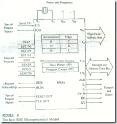
Figure 8 represents the hardware model with the logic pinout of the 8085. The six categories of the signals are address bus, data bus. control (and status) signals. external requests, request acknowledge, and power and frequency signals. In ad­dition, the 8085 has two signals for serial I/O.

microproccessor-architecture&memory-interfacing-19_03

FIGURE 8

The Intel 8085 Microprocessor Model

microproccessor-architecture&memory-interfacing-20_03

FIGURE 9

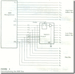
Demultiplexing the 8085 Bus

The 8085 has a 16-bit address bus: however. its low-order address bus is multiplexed with the data bus. These eight lines are time-shared by two functions; in the earlier part of a machine cycle. they are used for a low-order address, and in the later part for data. To interface this chip with memory (without any special features), these lines need to be demultiplexed (separated). The 8085 has a signal called ALE (Address Latch Enable), which can be used to demultiplex the bus. as shown in Figure 9. The ALE is asserted at the beginning of each machine cycle. when the bus has an address. Figure 9 shows that the ALE is used to latch the address. thus creating a separate low-order bus A7-A0. The Z80 does not need this signal because it has separate lines for the data and the address buses.

The 8085 has two status signals S0 and S1 to identify various machine cycles, and an IO/M͞ signal to differentiate between an I/O operation and a memory operation. In contrast. the Z80 identifies the Opcode Fetch cycle by asserting M͞1 , and has two separate signals (M͞R͞E͞Q and I͞O͞R͞Q) to identify memory and I/O op­erations. In the 8085, the control signals Memory Read/Write and I/O Read/Write are generated by ANDing IO/M͞ and control signals R͞D and W͞R.

Figure 8 shows that the 8085 provides five interrupt lines as external re­quests. out of which the TRAP is equivalent to the Z80 nonmaskable interrupt. The Z80 provides various additional interrupt modes through software.

8085 SOFTWARE MODEL

Figure 8 also shows the software model of the 8085. It includes one accumulator. a flag register, a general-purpose register array, and two 16-bit registers as mem­ory pointers (program counter and stack pointer). This model matches very well with the requirements of the microprocessor as a processing unit (Figure 2). The Z80 includes all the 8085 registers in addition to an alternate set of registers, index registers, and special-purpose registers.

National Semiconductor NSC80

The NSC800 is an 8-bit microprocessor manufactured by National Semiconduc­tor. It is a low-power CMOS device that combines features of the 8085 and the Z80. Because its power consumption is 5 percent of that of n-channel MOSFET (NMOS) devices. it is ideally suited for low-power or battery-operated ap­plications.

The NSC800 has a bus structure similar to that of the 8085: a multiplexed bus with the status signals S0, S1. and IO/M͞ . It has a powerful interrupt scheme that combines the 8085 signals and the Z80 interrupt modes. Its software model. instruction set, and mnemonics are identical with those of the Z80.

In summary. the NSC800 combines the software capability of the Z80 with the bus structure of the 8085; its hardware and software models match with the generalized model we developed in the previous topic.

Motorola MC6800

The MC6800 was developed at about the same time as the Intel 8080. The hard­ware model of this processor is similar to any other processor we have discussed, but it has a different internal architecture.

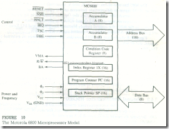
Figure 10 represents the 6800’s architecture. It has 16 address lines, 8 data lines, and fewer control (and status) signals than the Z80. The fewer control sig­nals result from the lack of peripheral-mapped I/O; all I/Os are interfaced as mem­ory-mapped I/Os. Therefore. the control signals in this processor need not differ­entiate between memory and I/O operations.

The other significant difference is in its internal architecture; it has two ac­cumulators, one flag register shown as the Condition Code Register, but no gen­eral-purpose registers. This processor uses external memory for storing interim

microproccessor-architecture&memory-interfacing-2_03

FIGURE 10

The Motorola 6800 Microprocessor Model

calculations and data bytes; it makes extensive use of memory referencing in its operations. The 6800 has simple timing and control signals; the clock period is the same as the machine cycle.

The 6809 is the latest improved version of the 6800 family; however. its ma­chine code is not compatible with that of the 6800. Its internal architecture is similar to that of the 6800, except it has an additional stack pointer, an additional index register. and a register to be used for referencing memory. The basic design philosophy is the same as that of the 6800, but it has eliminated some limitations of the 6800.

Review of 8-bit Microprocessors

In the last section, we examined the architectures of three microprocessors and occasionally compared them with the Z80. Now we can easily conclude that the architectures of various 8-bit microprocessors have similar patterns and can be represented by the hardware and the software models developed in the last chap­ter. We can classify these processors into two categories: one group, including the Z80, the 8085, NSC800, is register-oriented; the group including the 6800 and the 6809 is memory-reference-oriented.


SOME PUZZLING QUESTIONS AND THEIR ANSWERS

After reading the previous sections. the reader may have many unanswered ques­tions. One of the primary reasons for this predicament is that the microprocessor is a programmable and complex device. It interacts with external devices such as memory and I/Os. and some questions cannot be answered until we discuss these other devices. Similarly. some questions will remain unanswered until we start using instructions and writing programs. However. there are some questions that we should answer immediately. 

1. How does the Z80 microprocessor know where to begin after the power is turned on?

Most microcomputer systems have built-in power-on reset circuits , meaning that when the power is turned on, the microprocessor is reset and its program counter is cleared to the address 0000H , address 0000H is placed on the address bus and the instruction stored at that location determines what happens next.

2. How does the Z80 know what operation to perform first (Memory Read/Write , or I/O Read/Write)?

The first operation is always an Opcode Fetch.

3. How does the microprocessor differentiae between an opcode and a data byte ?

When the first opcode is fetched and decoded in the instruction register, the microprocessor recognizes the number of bytes that must be read from memory for the complete instruction. The instructions can range from 1 to 4 bytes in length. Figure 5. for example. contains a 2-byte instruction (3E and Data). and the second byte is always considered Data. If that second byte is omitted by mistake. the Z80 will interpret whatever is in that memory location as Data. The byte after the Data will be treated as the next instruction. The microprocessor is a sequential machine: it goes from -one memory location to the next unless in­structed to do otherwise.

4. What is the use of the M͞1 signal? It looks as if it will not be connected to any device.

This signal serves two purposes: (1) it differentiates the Opcode Fetch cycle from other operations. and (2) it can be used to generate the Interrupt Acknowledge signal.

5. if flags are individual flip-flops. can they be observed on an oscilloscope?

No, they cannot be observed on an oscilloscope; these flip-flops are internal and not connected to any of the external pins. However, they can be examined by storing them on the stack memory) (see Topic 10).

6. is the number of T-states required for a given machine cycle constant?

No, But most Opcode Fetch machine cycles require four T-states, and Mem­ory Read/Write and I/O Read/Write machine cycles, generally, take three or four T-states, However, there are some exceptions.

7. How does one recognize The machine cycles in a given instruction ?

The number of machine cycles and the T-states required for those machine cycles are listed in the instruction set , There is a repetitive pattern and one can use the following guidelines.
· The number of machine cycles in an instruction indicates how many times the microprocessor must access memory or I/O.
· The first machine cycle in an instruction is always Opcode Fetch.
· The microprocessor must read all the bytes (codes) from memory before it can execute an instruction .
For example, a 3-byte instruction requires at least three machine cycles. The unconditional Jump instruction is a 3-byte instruction with 10 (4,3,3) T-states; it consists of one opcode and a 16-bit address of the jump location. Therefore , by examining the number of T – states, we can easily classify the machine cycles of the Jump instruction as one 0 code Fetch and two Memory Read.
Another example is ADD . 32 (add a byte 32H to the contents of the accumulator). This is a 2-byte instruction with 7 (3) T-states. By examining the number of bytes and the number of T-states. We can conclude that it must have two machine cycle -the first is Opcode Fetch, and the second is Memory Read. The addition is performed inside the processor, and it does not need any addi­tional information from memory or I/O.

8. How does recognize machine cycles in an instruction when the number of bytes is not the same as the number of machine cycles?

One has to examine the number of bytes. T-states. and the operation being performed. For example, the instruction LD (2050H), A has three bytes and 13 (4, 3. 3. 3) T-states; it copies the contents of the accumulator into the memory loca­tion 2050H .The processor must read the entire instruction first: therefore. the first must be Opcode Fetch, followed by two Memory Read cycles. This accounts for ten T-states. In the remaining three states , the processor must write (copy) the contents of the accumulator into the memory location 2050H ;therefore. it must be the Memory Write cycle.
 

Generating Control Signals

After examining the concepts summarized at the end of the previous section, we may need to generate additional control signals.

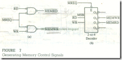
1. To read from memory, the M͞R͞E͞Q and the R͞D signals are necessary, and to read from an input device, the I͞O͞R͞Q and the R͞D are necessary; all these sig­nals are active low. As a design practice, the M͞R͞E͞Q is generally combined with a decoded address (discussed in Topic4). and R͞D is connected directly to the memory chip. However, control signals R͞D and W͞R can also be com­bined with M͞R͞E͞Q and I͞O͞R͞Q to generate additional signals. We can generate active low Memory Read (M͞E͞M͞R͞D) signal either by ANDing these signals in a negative NAND gate as shown in Figure 7(a) or by using a 2-to-4 decoder as shown in Figure 7(b). The decoder is enabled by the M͞R͞E͞Q and has R͞D and W͞R signals as input. Both inputs cannot be active at the same time; when one is low, the other will remain high, When R͞D is active low, the input is 0 1 , and the output O1 goes active as M͞E͞M͞R͞D.

2. To write into memory, the M͞R͞E͞Q and the W͞R signals are necessary. and to write a data byte to an output device, the I͞O͞R͞Q and W͞R signals are necessary;

microproccessor-architecture&memory-interfacing-1_03

FIGURE 7

Generating Memory Control Signals

all these signals are active low. We can generate active low Memory Write (M͞E͞M͞W͞R) signal by ANDing M͞R͞E͞Q and W͞R signals in a negative NAND gate as shown in Figure 7(a) or by using the decoder as shown in Figure 7(b). Similarly, I͞O͞R͞D (I/O Read) and I͞O͞W͞R (I/O Write) signals can be gen­erated; this is discussed in Topic5.


MACHINE CYCLES AND BUS TIMINGS

MACHINE CYCLES AND BUS TIMINGS

The Z80 microprocessor is designed to execute 158 different instruction types. Each instruction has two parts: operation code (known as opcode) and operand. The opcode is a command such as Add, and the operand IS an object to be oper­ated on, such as a byte or the contents of a register. Some instructions are 1-byte instructions. and some are multibyte instructions. To execute an instruction, the Z80 needs to perform various operations such as Memory Read/Write and I/O Read/Write. However, there is no direct relationship between the number of bytes of an instruction and the number of operations the Z80 has to perform. For ex­ample, the instruction to send the contents of the accumulator to the output port 10H,is a 2-byte instruction: OUT (10H), A.

  • Byte 1: OUT → This is the opcode to output data.
  • Byte 2: (10H*) , A → This is the operand to specify that the byte should be sent from the accumulator to port 10H .

(A hexadecimal number in an instruction is shown as a number followed by the letter H. )

But the Z80 has to perform three operations:

(1) read Byte 1 from memory,

(2) . read Byte 2 from memory,

(3) send data to port 10H .

In the previous section. numerous Z80 signals and their functions were de­scribed. Now we need to examine these signals in conjunction with execution of , individual instructions and their operations. This task may appear overwhelming

at the beginning; fortunately. all instructions are divided into a few basic opera­tions called machine cycles. and these machine cycles are divided into precise system dock periods.

The microprocessor external communication functions can be divided into three basic categories:

1. Memory Read and Write.

2. I/O Read and Write.

3. Request Acknowledge .

These functions are further divided into various operations (machine cycles) as shown in Table 3.1. Each instruction consists of one or more of these machine cycles. and each, machine cycle is divided into T-states .

To understand various operations. we need to define three terms: instruction cycle. machine cycle. and T-state.

Instruction cycle is defined as the time required to complete the execution of an instruction The Z80 instruction cycle consists of one to six machine cycles or one to six operations.

Machine cycle is defined as the time required to complete one operation of accessing memory. accessing I/O. or. acknowledging an external request. This cycle may consist of three to six T-states.

T-state is defined as one subdivision of the operation performed in one clock period. These subdivisions are internal states synchronized with the system clock. and each T-state is precisely equal to one clock period. The terms T-state and clock period are often used synonymously.

In this topic. we focus on the first three operations listed in Table 3.1- Opcode Fetch, Memory Read, and; Memory Write-and examine the signals on various buses in relation to the system clock. In the next topic. we will use these timing diagrams to interface memory with the Z80 microprocessor. Similarly, we will discuss timings of other machine cycles in later topics in the context of their applications. For example, I/O Read/Write machine cycles will be discussed in Topic 5 and Interrupt Acknowledge will be discussed in Topic 12.

TABLE 3.1

The Z80 Machine Cycles and Control Signals

Machine Cycle

1

M͞R͞E͞Q

IO͞R͞Q

R͞D

W͞R

Opcode Fetch (M͞1 )

0

0

1

0

1

Memory Read

1

0

1

0

1

Memory Write

1

0

1

1

0

I/O Read

1

1

0

0

1

I/O Write

1

1

0

1

0

Interrupt Acknowledge

0

1

0

1

1

Non-maskable Interrupt

0

0

1

0

1

Bus Acknowledge (B͞U͞S͞A͞K = 0)

1

Z

Z

Z

Z

NOTE: Logic 0 = Active. Logic 1 = Inactive. Z = High Impedance

Opcode Fetch Machine Cycle M͞ 1 )

The first operation in any instruction is opcode fetch. The microprocessor needs to get (fetch) this machine code from the memory register where it is stored before the microprocessor can begin to execute the instruction. The opcode fetch oper­ation and its timing signals are illustrated in Example 1.

Example 1

The accumulator of the Z80 microprocessor holds the data byte 9FH . and the code for instruction LD B, A (opcode) 0 1 0 0 0 1 1 1 (47 H) is stored in memory location 2002H This is a I-byte instruction. and when this opcode is executed. the contents of the accumulator will be copied into register B. List the sequence of events that takes place to execute this machine code and illustrate the signals on various buses in relation to the system clock .

Solution

We assume here that the Z80 has already completed the execution of the code in memory location 2001H and the program counter holds the address 2002H Before the Z80 can execute the opcode, it needs to fetch the code from the memory location, To fetch the opcode, the Z80 performs the following steps:

1. The Z80 places the contents of the program counter (2002H) on the address

bus, and increments the program counter to the next address. 2003H:The pro­gram counter always points to the next byte to be executed.

2.The address is decoded by the external decoding circuit, and the register 2002H is identified.

3.The Z80 sends the control signals (M͞R͞E͞Q and R͞D) to enable the memory out­put buffer.

4.The contents of the memory register (opcode 47H) are placed on the data bus and brought into the instruction decoder of the microprocessor .

5. The Z80 decodes the Z80 ode and executes the instruction, meaning it copies the contents of the accumulator into register B.
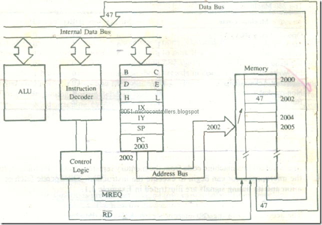
microproccessor-architecture&memory-interfacing-10_03

FIGURE 3

Z80 Memory Read Operation

Figure 3 shows how the Z80 fetches the opcode using the address and the data buses and the control signal. Figure 4 shows the timing of the Opcode Fetch machine cycle in relation to the system’s clock. The address bus in Figure 4 is shown as two parallel lines. This is a commonly used practice to represent logic levels of groups of lines; some lines are high and others are low, and the crossover of the lines indicates that a new address is being placed on the address bus . the high impedance state is shown by a straight line as in the data bus ( D7 – D0 ) .The of these signals are given below.

1. Figure 4 shows that the Opcode Fetch cycle is completed in four clock pe­riods or T-states. This machine cycle is also identified, as the M1 cycle.

2. At the beginning of the first clock period T1 , the control signal M͞1 goes low

and the contents of the program counter (2002H) are placed on the address bus .

3. After the falling edge of T1 , the Z80 asserts two control signals-M͞R͞E͞Q and R͞D, both active low The M͞R͞E͞Q indicates that it is a memory-related operation, and R͞D suggests that it is a Read operation. Both signals are necessary to read from memory.

4. The internal decoder of the memory and the Chip Select circuit (not shown in Figure 4) decode the address and identify register 2002H The control signals
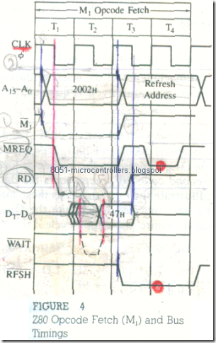
microproccessor-architecture&memory-interfacing-11_03

FIGURE 4

Z80 Opcode fetch (M1) and Bus Timings

SOURCE: Courtesy or Zilog Inc.

(adapted).

M͞R͞E͞Q and R͞D are used to enable the memory output buffer. The data bus. which was in high impedance state. is activated as an input bus (to the micro- processor) shortly after the .leading edge of T2. After the falling edge of T2. memory places its register contents (47H) on the data bus.

5. At the leading edge of T3, the data on the data bus are read, and the control signals become inactive .

6. During T3 and T4 , when the instruction decoder in the microprocessor decodes and executes the opcode. These are internal operations and cannot be observed on the data bus.

The following two steps are irrelevant to the present problem; however. they are included here as part of the M1 cycle.

7. During T3 and T4 when the Z80 is performing internal operations. the low order address bus is used to supply a 7-bit address for refreshing dynamic memory . If the system includes dynamic memory, this operation simplifies its in­terfacing hardware. This aspect of the M1 cycle will be discussed again when

we illustrate interfacing of dynamic memory (Topic 16).

8. Figure 4 shows the signal called W͞A͞IT. The Z80 samples the Wait line during T2 and if it is forced low by an external device (such as memory or I/O). the Z80 adds Wait states (clock cycles) to extend the machine cycle and continues to add clock cycles until the Wait signal goes high again. This technique is used

to interface memories with slow response time and will be discussed again in Topic 16.

Memory Read Machine Cycle

The second machine cycle we want to illustrate is Memory Read. As explained in the next example, this cycle is quite similar to the Opcode retch cycle.

Example 2

Two machine codes-0 0 1 1 1 1 1 0 (3EH) and 1 0 0 1 1 1 1 1 (9FH)-are stored in memory locations 2000H and 2001 H , respectively, as shown below. The first machine code (3EH) represents the opcode to load a data byte into the accumulator, and the second code (9FH) represents the data byte to be loaded into the accu­mulator, Illustrate the bus timings as these machine codes are executed, and cal­culate the time required to execute the Opcode Fetch and the Memory Read cycles and the entire instruction cycle if the clock frequency is 4 MHz.

Address Machine Code Instruction Comment

microproccessor-architecture&memory-interfacing-12_03

Solution

This instruction consists of two bytes ; the first is the opcode. and the second is the data byte. The Z80 must first read these bytes from memory and thus requires at least two machine cycles. The first machine cycle is Opcode Fetch. and the second machine cycle is Memory Read, as shown in Figure 5. These cycles are described in the following list.

1.The first machine cycle (Opcode Fetch) is identical in bus timings with the machine cycle illustrated in Example 1. except for the bus contents. The address bus contains 2000H , and the data bus contains the opcode 3EH . when the Z80 decodes the opcode during the T3 state, it realizes that a second byte

must be read.

2. After the completion of the Opcode Fetch cycle, the Z80 places the address

2001H on the address bus and increments the program counter to the next address. 2002H ,To differentiate the second cycle from the opcode Fetch cycle. the M1 signal remains inactive (high).

3. After the falling edge of T1 of the Memory Read cycle, the control signals M͞R͞E͞D and R͞D are asserted. These signals, along with the memory address, are used to identify the register 2001H and enable the memory chip .

4. After the leading edge of T3 , the Z80 activates the data bus as an input bus ; memory places the data byte 9FH on the data bus, and the Z80 reads and stores . the byte in the accumulator during T3 .

5. After the falling edge of T3 , both control signals become inactive (high). and at

the end of T3 , the next machine cycle begins.
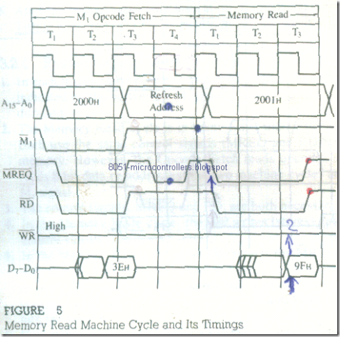
microproccessor-architecture&memory-interfacing-13_03

FIGURE 3.5

Memory Read Machine Cycle and Its Timings

The execution times of the Memory Read machine cycle and the instruction cycle are calculated as follows:

Clock Frequency f = 4 MHz

T-state = Clock Period (1/f) = 0.25 µs

Execution Time for Opcode Fetch: (4 T) x 0.25 = 1.0 µs

Execution Time for Memory Read: (3 T) x 0.25 = 0.75 µs

Execution Time for Instruction: (7 T) x 0.25 == 1.75 µs

Memory Write Cycle

Now we want to illustrate the third machine cycle: Memory Write. This machine cycle writes or stores data in a specified memory register as shown in the following example.

Example 3

The HL register holds the address 2350H , and the accumulator has the data byte 9FH , The instruction code 0 1 1 1 0 1 1 1 (77H) is stored in memory location 2003H , When this code is executed, it stores the contents of the accumulator in the memory location indicated by the address in the HL register. Illustrate the bus con­tents and timings as this instruction is being executed.
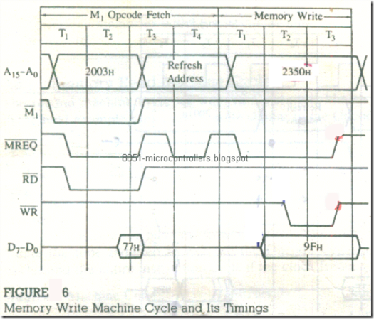
microproccessor-architecture&memory-interfacing-14_03 

FIGURE 6

Memory Write Machine Cycle and Its Timings

Instruction: LD (HL), A ;Copy contents of the accumulator into memory location, the address of which is stored in HL register.

Solution

This is a one-byte instruction with two machine cycles: Opcode Fetch and Memory Write . In the first machine cycle, the Z80 fetches the code(77H), and in the second machine cycle, it copies the byte 9FH from the accumulator into the mem­ory location 2350H , The timings of these machine cycles are shown in Figure 6 and explained be row.

1. In the Opcode Fetch machine cycles , the Z80 places the address 2003H on the address bus and gets the code 77H by using the control signals M͞R͞E͞Q and R͞D as in the previous examples. The program counter is also incremented to the next address, 2004H

2. During the T3 and T4 states, the Z80 decodes the machine code 77H and pre­pares for the memory write operation .

3. At the beginning of the next machine cycle (Memory Write). it places the con­tents (2350H) of the HL register on the address bus. At the falling edge of T3 M͞R͞E͞Q goes low and the data byte 9FuJrom the accumulator is placed on the data bus.

4. After allowing one T-state (after M͞R͞E͞Q) to stabilize the address. the Z80 as­serts the control signal Write (W͞R), which is used to write the data byte at the address shown on the address bus.

5. After the falling edge of T3 , both control signals become inactive, and one-half T-state later, the data bus goes into high impedance state .

Review of Important Concepts

1. In each instruction cycle, the first operation is always Opcode Fetch, and it is indicated by the active low M͞1 signal, This cycle can be four to six T-states in duration.

2. The Memory Read cycle is in many ways similar to the Opcode Fetch cycle, Both use the same control signals (M͞R͞E͞Q and R͞D) and read contents from memory. However, the Opcode Fetch reads opcodes and the Memory Read reads 8-bit data or addresses; the two machine cycles are differentiated by the M͞1 signal.

3. The control signals, MREQ and RD, are both necessary to read from memory .

4. In the Memory Write cycle, the Z80 writes (stores) data in memory using the

control signals M͞R͞E͞Q and W͞R .

5. In the Memory Read cycle, the Z80 asserts the M͞R͞E͞Q and R͞D signals to en­able memory, and then the addressed memory places the data on the data bus; on the other hand, in the Memory Write cycle, the Z80 asserts the M͞R͞E͞Q. places the data byte on the data bus. and then asserts the W͞R signal to write into the addressed memory.

6. Generally, the Memory Read and Write cycles consist of three T-states; how­ever, they can take four T-states in some instructions. The Memory Read and Write cycles will not be asserted simultaneously; the microprocessor cannot read and write at the same time.


Z80 HARDWARE AND PROGRAMMING MODELS

Z80 Microprocessor Architecture

The Z80 is one of the most versatile and widely used 8-bit microprocessors, and many micro­processor-based systems are designed around the Z80. The Z80 chip includes most of the logic circuitry for performing computing tasks and necessary bus signals. This topic discusses the Z80 architecture in terms of the generalized MPU discussed in the previous topic .

This topic describes the Z80 hardware model; it shows logic pinout of the chip and classifies the signals in various groups accord­ing to their functions. Similarly, the topic in­cludes a brief description of programming reg­isters and flags. The hardware model lists the operations the Z80 frequently performs and describes how the Z80 communicates with mem­ory and I/Os by using various buses. These op­erations are illustrated in terms of machine cycles and logic levels of the buses in relation to the system clock.

Finally, the topic includes the discus­sion of similar 8-bit microprocessors in terms of the generalized model developed in the last topic and compares them with the Z80.

OBJECTIVES

· List the functional groups of the Z80 signals.

· Define the address bus. the data bus, and the control signals. and explain their functions.

· List the types of external signals and explain their purposes.

· Identify the Z80 programming registers and flags.

· List three categories of the Z80’s operations.

· Explain the terms instruction cycle, machine cycle, and T-state.

· List the steps the Z80 performs to execute the Opcode Fetch, the Memory Read, and the Memory Write cycles. and explain their functions.

· Show the bus contents and the appropriate control signals in reference to the system clock when these machine cycles are exe­cuted.

· Describe the 8085, the NSC800. and the 6800 microprocessors in terms of the generalized MPU and compare them with the Z80.

Z80 HARDWARE AND PROGRAMMING MODELS

The Z80 hardware model described in this section represents the microprocessor unit (MPU) as defined in Topic 2. The 280 microprocessor almost qualifies as an MPU. except that an external oscillator circuit is required to provide the op­erating frequency and appropriate control signals need to be generated to com­municate with memory and I/O. In the following sections. we describe the Z80 microprocessor in relation to the model we developed in the previous topic. Then we examine the timing involved in reading an instruction from memory and generate the necessary control signals by using appropriate logic gates.

Z80 Hardware Model

The Z80 is a general-purpose 8-bit microprocessor with 16 address lines and re­quires a single +5 V power supply. It is housed in a 40-pin dual-in-line (DIP) package. The different versions of Z80 microprocessors such as Z80, Z80A, Z80B, and Z80H are rated to operate at various frequencies ranging from 2.5 MHz to 8 MHz. Even though the Z80 instruction set is upward compatible with the Intel 8080 set. neither of these microprocessors are pin compatible.

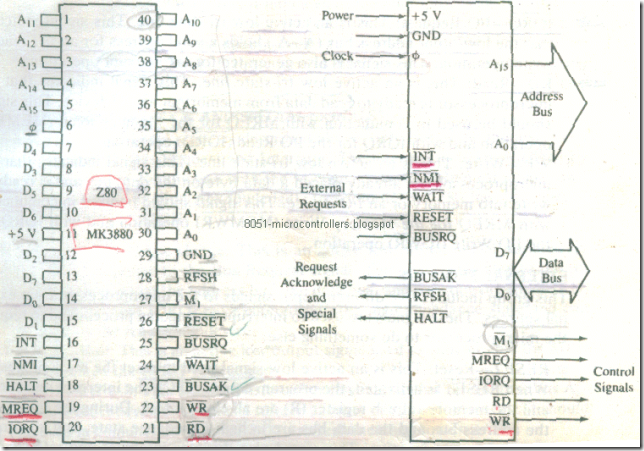
Figure 1 shows the pin configuration of the Z80 microprocessor and its hardware model with logic signals. All the signals can be classified into six groups: (1) address bus, (2) data bus. (3) control signals, (4) external requests, (5) request acknowledge and special signals, and (6) power and frequency signals. This Z80 hardware model matches the hardware model of the generalized MPU described in Topic 2. The specific details of these signals follow.

microproccessor-architecture&memory-interfacing-3_03

ADDRESS BUS

The Z80 has 16 tri-state signal lines. A15-A0 , known as the address bus. These lines are unidirectional and capable of addressing 64K (216) memory. The address bus is used to send (or place) the addresses of memory registers and I/O devices.

DATA BUS

The data bus consists of eight tri-state bidirectional lines D7-D0 and is used for data transfer. On these lines, data can flow in either direction-from the micro­processor to memory and I/Os or vice versa.

CONTROL SIGNALS

This group consist of five individual output lines: three can be classified as status signals indicating the nature of the operation being performed, and two as control signals indicating the nature of the operation being performed , and two as control signals to read from and write into memory or I/ os .

· M̅1__ Machine Cycle one: This is an active low signal indicating that an opcode is being fetched from memory . this signal is also used in an interrupt operation to generate an interrupt acknowledge signal , which will be explained in topic 12 .

· M͞R͞E͞Q __ Memory Request: This is an active low tri-state line. This signal indicates that the address bus holds a valid address for a memory read or write operation.

· I̅O̅R̅Q̅ __ I/O Request: This is an active low tri-state line. This signal indicates that the low-order address bus (A7 –A0) holds a valid address for an I/O read or write operation. this signal is also generated for an interrupt operation .

· R̅D̅__Read: This is an active low tri-state line. This signal indicates-that the microprocessor is ready to read data from memory or an I/O device . This signal should be used in conjunction with MREQ for the Memory Read (M̅E̅M̅R̅D̅) operation and with IORQ for the I/O Read (I̅O̅R̅D̅) operation.

· W̅R̅ __ Write : This is an active low tri-state line. This signal indicates that the microprocessor has already placed a data byte on the data bus and is ready to write into memory or an I/O device . This signal should be used in conjunction with MREQ for the Memory Write (M̅E̅M̅W̅R̅) operation and with IORQ for the I/O Write (I̅O̅W̅R̅) operation.

EXTERNAL REQUESTS

This group includes five different input Signals to the microprocessor from exter­nal sources. These signals are used to interrupt an ongoing process and to request the microprocessor to do something else.

· R̅E̅S̅E̅T̅ __ Reset: This is an active low signal used to reset the microprocessor.

When R̅E̅S̅E̅T̅ is activated. the program counter (PC), the interrupt register (I), and the memory refresh register (R) are all cleared to 0 .During the reset time. the address bus and the data bus are in high impedance state , and aII control signals become inactive . This signal also disables interrupt and refres . The R̅E̅S̅E̅T̅ signal can be initiated by an external key or switch and must be active at least for three clock periods to complete the reset operation.

·

INT __Interrupt Request

This is an active low signal. initiated by an I/O device to interrupt the microprocessor operation . when the microprocessor accepts the interrupt request, it acknowledges by activating the lORQ signal during the M1 cycle. The INT signal is maskable , meaning It can be disabled trough a software instruction. The interrupt process will be fully discussed in topic 12.

·

NMI__ Nonmaskable Interrupt

: This is a nonmaskable interrupt; it cannot be disabled. It is activated by a negative edge-triggered signal from an external source. This signal is used primarily for implementing emergency procedures.

There is no signal or pill to acknowledge this signal; it is accepted provided the Bus Request signal is inactive. (See topic 12 for details.)

· BUSRQ__Bus Request: This is an active low signal initiated by external I/O devices such as the DMA (Direct Memory Access) controller. An I/O device can send a low signal to BUSRQ to request the use of the address bus . the data bus, and the control signals . The external device can use the buses, and when its operations are complete, it returns the control to the microprocessor. This signal is used primarily for the direct memory access technique to be discussed in topic 16.

· WAIT__Wait: This is an active low signal and can be used by memory or I/O devices to add clock cycles to extend the Z80 operations . This signal is used when the response time of memory or I/O devices is slower than that of the

Z80. When this signal goes low, it indicates to the microprocessor that the ad­dressed memory or I/O device is not yet ready for data transfer. As long as this signal is low, the Z80 keeps adding cycles to its operation. The signal will be discussed in topic 16 to illustrate how to interface slow memory chips using wait slates.

REQUEST ACKNOWLEDGE AND SPECIAL SIGNALS

Among the five external requests described above, only two of the requests need acknowledgment: Bus Request and Interrupt . The interrupt is acknowledged by the I̅O̅R̅Q̅ signal in conjunction with the M1 signal. The Bus Request is acknowledged by a B̅U̅S̅A̅K̅ (Bus Acknowledge). In addition. the Z80 has two special signals: H̅A̅L̅T̅ and R̅F̅S̅H̅.

  • B̅U̅S̅A̅K̅__Bus Acknowledge: This is an active low output signal initiated by the Z80 in response to the Bus Request signal. This signal indicates to the requesting device that the address bus, the data bus, and the control signals (R̅D̅, W̅R̅. M̅R̅E̅Q̅, and I̅O̅R̅Q̅) have entered into the high impedance state and can be used by the requesting device.
  • H̅A̅L̅T̅-Halt: This is an active low output signal used to indicate that the MPU has executed the HALT instruction.
  • R̅F̅S̅H̅-Refresh: This is an active low signal indicating that the address bus A6– A0 (low-order seven bits) holds a refresh address of dynamic memory; it should be used in conjunction with M̅R̅E̅Q̅ to refresh memory contents.

POWER AND FREQUENCY SIGNALS

This group includes three signals as follows:

  • Φ – Clock: This pin is used to connect a single phase frequency source. The Z80 does not include a clock circuit on its chip; the circuit must be built separately.
  • + 5 V and GND – These pins are for a power supply and ground reference; the Z80 requires one + 5 V power Source.

Z80 Programming Model

In the last topic, we developed a model to represent the internal structure of the MPU to process data, shown in Figure 3. Now, we will describe a similar model of the Z80 microprocessor as shown in Figure 2. The model includes an accumulator and a flag register, general-purpose register arrays, registers as mem­ory pointers, and special-purpose registers. These registers and their functions are briefly described in the following sections; topic 6 provides greater detail.

GENERAL-PURPOSE REGISTERS

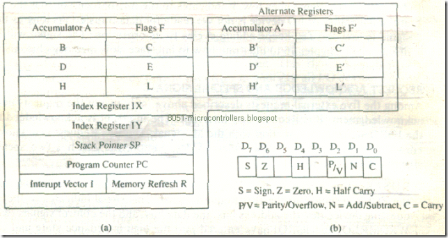
The Z80 microprocessor has six programmable general-purpose registers named B, C, D, E, H, and L, as shown in Figure 2. These are 8-bit registers used for storing data during the program execution. They can be combined as register pairs-BC, DE, HL-to perform 16-bit operations or to hold memory addresses. The programmer can use these registers to load or copy data.

microproccessor-architecture&memory-interfacing-6_03

ACCUMULATOR

The accumulator is an 8-bit register that is part of the arithmetic logic unit (ALU) and is also identified as register A. This register is used to store 8-bit data and to perform arithmetic and logic operations. The result of an operation performed in the ALU is stored in the accumulator.

FLAG REGISTER

The ALU includes six flip-flops that are set or reset according to data conditions after an ALU operation, and the status of these flip-flops, also known as flags, is stored in the 8-bit flag register. For example, after an addition in which the result generates a carry, the carry flip-flop will be set and bit Do in the flag register will show logic 1. The bit position of each flag is shown in Figure 2(b); bits D5 and D3 are unused.

Among the six flags. the H (Half-Carry) and N (Add or Subtract) flags are

used internally by the microprocessor for BCD (Binary Coded Decimal) opera­tions. Each of the remaining four flags-S (Sign), Z (Zero), P/Y (Parity or Over­flow). and C (Carry)-has two Jump or Call instructions associated with it: one when the flag is set and the other when the flag is reset. The details of these flags and their critical importance in programming and decision making are discussed in Topic 6.

ALTERNATE REGISTER SET

In addition to the general-purpose registers, the accumulator, and the flag register.

the Z80 includes a similar set of alternate registers designated as B’, C’, D’, E’, H’, L’, the accumulator A’, and the flag register F’. These registers are not di­rectly available to the programmer: however. the exchange instructions can ex­change information of register pairs with the respective alternate register pairs.

16-BIT REGISTERS AS MEMORY POINTERS

The Z80 microprocessor includes four 16-bit registers. and these registers are used to hold memory addresses: thus. they are classified here as memory pointers. The primary function of memory is to store instructions and data, and the micropro­cessor needs to access memory registers to read these instructions and data. To access a byte in a memory location, the microprocessor identifies the memory location by using the addresses in these memory pointers. The Z80 has two such specific 16-bit memory pointers, IX and IY. called index registers.

Stack Pointer (SP)

This is also a 16-bit register that is used to point to the memory location called the stack. The stack is a defined area of memory locations in R/W memory, and the beginning of the stack is defined by loading a 16-bit address in the stack pointer. We will discuss the concept of the stack memory in detail when we introduce the topic of subroutines in Topic 10.

Program Counter

(PCL This register functions as a 16-bit counter. The micropro­cessor uses this register to sequence the execution of instructions. The function of the pro ram counter is to point to the memory address from which the next byte is to be fetched. When the microprocessor places an address on the address bus to fetch the byte from memory. it then increments the program counter by one to point to the next memory location.

Special. Purpose Registers The Z80 microprocessor includes two special-purpose registers that are generally absent in other 8-bit microprocessors. These registers are shown in Figure 2 as the Interrupt Vector Register (I) and the Memory Re­fresh Register (R). The functions of these registers will be described in later topics.