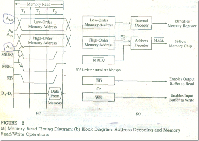
In Topic 3, we showed t e timing diagrams and the Z80 bus contents When an opcode or a data byte is fetched from memory. To read from memory, the Z80 performs the following steps, as shown in Figure 2(a) :
1- Places a 16-bit address on its address bus (shown as high- and low order addresses )
2- Asserts the M͞R͞E͞Q to indicate that the address bus holds a valid address
3- Asserts the R͞D signal low to indicate that it wants to read .
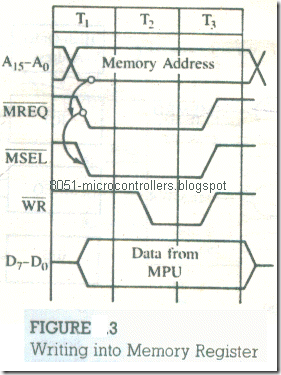
To write into memory, the Z80 performs the following steps, as shown in Figure 3:
1- Places a 16-bit address on its address bus
2- Asserts M͞R͞E͞Q and places data on the data bus .
3- Asserts W͞R signal
To understand and design an interface circuit, we need to match the memory requirements with the Z80 read/write operations.
FIGURE 4.2
(a) Memory Read Timing Diagram; (b) Block Diagram: Address Decoding and Memory Read/Write Operations
Basic Concepts in Memory Interfacing
The primary function of memory interfacing is to allow the microprocessor to read from and write into a given register of a memory chip To perform these operations, the microprocessor should
-
be able to select the chip.
-
Identify t the register
3. Enable the appropriate buffer.
Let us examine the timing diagram of the memory read operation – figure 2(a) – in order to understand how the Z80 can read from memory in figure 2(a) the address bus is divided into two segments low order A0-AI.O and high order AH1-A15 to explain the decoding concepts the number of address lines represented by the ALO and AH1 varies according to the size of the memory chip .
The Z80 places a 16-bit address on the address bus and with this address only one register should be selected for the memory chip in figure 1 only ten address lines are required to identify 1.024 registers therefore we can connect the low-order address lines A9-A0 (ALO = A9 ) of the Z80 address bus to the memory chip.
FIGURE 3
Writing into Memory Register
The internal decoder of the memory chip will identify and select the register, as shown in Figure 2(b) .
2. The remaining Z80 address lines A15-A10 (AH1 = A10) should be decoded to generate a Chip-Select (C͞S) signal unique to that combination of address logic .
3. The Z80 provides two signals: M͞R͞E͞Q and R͞D. The M͞R͞E͞Q can be combined with decoded address pulse (C͞S) to generate a Memory Select (M͞S͞E͞L) to select the memory chip .
4. The microprocessor asserts the control signal R͞D, enables the output buffer of memory, and reads the data byte. Figure 2(a) also shows that memory must place the data byte on the data bus at the beginning of T3 .
To write into a register, the microprocessor performs similar steps. Figure 3 shows the Memory Write cycle. In the Write operation, the Z80 places the address and data, and asserts the M͞R͞E͞Q signal. After allowing sufficient time for data to become stable it asserts the Write (W͞R) signal, The W͞R signal enables the input buffer of the memory chip-and store the byte in the selected register.
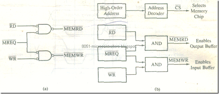
An alternative to generating the M͞S͞E͞L signal (Step 3 in Memory Read) to select the memory chip is generate the control signals M͞E͞M͞R͞D and M͞E͞M͞W͞R by-combining the M͞R͞E͞Q , R͞D, and W͞R as shown in Figure 4). The M͞E͞M͞R͞D can be used to enable the output buffer to read from memory; the M͞E͞M͞W͞R can be used to enable the input buffer to Write into memory, and the decoded address pulse (C͞S) can be used to select the chip as shown in Figure 4(b).
To interface memory with the microprocessor, we can summarize the above steps as follows:
1. Connect the required address lines of the address bus to the address lines of the memory chip.
2. Decode the remaining address lines of the address bus to generate the Chip
Select signal, as discussed in the next section (4).
FIGURE 4
(a) Generating Control Signals; (b) Block Diagram: Alternative Approach to Memory Read/Write Operations
3. Generate the signal Memory Select (M͞S͞E͞L) by combining the decoded address pulse C͞S and the M͞R͞E͞Q , and the MSEL to select the memory chip .
4. Connect the Z80 R͞D and W͞R control signals to the R͞D and WR memory signals to enable memory buffers.
5 .An alternative procedure is to generate control signals M͞E͞M͞R͞D and M͞E͞M͞W͞R by combining R͞D and W͞R signals with the M͞R͞E͞Q and to use them to enable appropriate buffers. The decoded address pulse (C͞S) is used to select the memory chip.
Address Decoding
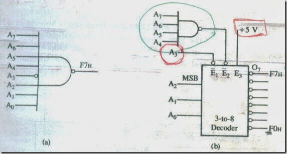
The process of address decoding should result in identifying a register with a given address ; we should be able to generate a unique pulse for that address for example in figure 5(a) the output of the NAND gate goes low (active) only when the address on the address lines is F7H no other address can cause the output of the gate to go low this process is called decoding the address we can also use a decoder for address decoding as discussed bolo war a PROM (programmable Read only memory ) as discussed in topic 16 .
Figure 5(b) shows a 3-to-8 decoder and a 4-input NAND gate the decoder has three enable lines one active high and two active low the enable line E1 is connected to address lines A2,A1, and A0 are inputs to the decoder, and the enable line E3 is tied high and is not being used here for decoding .
In this decoder circuit three input lines can have eight different logic combinations from 000 ot 111; each input combination can be identified by the corresponding output line if enable lines are active for example if the input is 0 0 0, O0 goes low (others remain high) and if the input is 1 1 0, O6 goes low , to Activate the enable line E͞1 , A3 should be low , and to activate E͞2 , address lines A7 – A4 should be high , causing the output of the NAND gate to go low , if the input to the decoder is 1 1 1 , the output line O7 of the decoder will go low , thus decoding the address F7H .
FIGURE 5 . Address Decoding
This 3-to-8 decoder can identify or decode eight addresses from FOH to F7H as shown in Figure 5(b). We will use this address decoding scheme, for interfacing memory chips in the following illustrations (Sections 2 and 3).


