Memory is an integral part of a microprocessor based system, and in this topic our focus will be on how to interface a memory chip with the microprocessor. We will examine memory structure and requirements to read from it an write into it, We then compare those requirements with those of the Z80 Memory Read and Write machine cycles, From that comparison, we will derive the basic steps necessary to interface memory.
This topic illustrates two .examples of interfacing memory chips, one EPROM and the other static R/W memory. The discussion includes analyses of the following: decoding circuits, memory maps, the concepts of fold back memory and absolute decoding. Finally, an example of memory design is illustrated to synthesize the interfacing concepts.
OBJECTIVES
-
List the requirements to read from memory.
-
List the steps initiated by the Z80 to read from and write into memory.
-
List the steps required to interface a memory chip with the Z80.
-
Analyze given EPROM and static R/W memory interfacing circuits and specify their memory address ranges.
-
Explain the terms absolute decoding and foldback memory.
-
Design a circuit to interface EPROM and R/W memory with the Z80 for given memory addresses.
INTERFACING MEMORY
While executing a program , the microprocessor needs to access memory frequently to read instruction codes and data stored in memory and the interfacing circuit enables that access. Memory has certain signal, requirements for writing into and reading from its registers. Similarly the microprocessor initiate a set of signals when it wants to communicate with memory . the interfacing process involves designing a circuit that will match the memory requirements with the microprocessor signals. In the following section, we examine memory structure and its requirements and also the Z80 Memory Read and Write machine cycles. Then we derive the basic steps necessary to interface memory with the Z80 .
Memory Structure and Its Requirements
Read/Write Memory (R/WM) is a group of registers to store binary information.
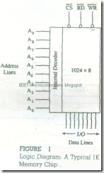
Figure 1 shows a typical R/W memory chip; it has 1024 registers, each of which can store eight bits indicated by eight I/O lines. the chip has ten address lines A9– A0 , one Chip Select C͞S, and two control lines : Read (R͞D) to enable the Output buffer and Write (W͞R) to enable the input buffer. Figure 4 also shows the internal decoder to decode the address lines. We may recall from Topic2 that to read from or write into one of the memory registers certain requirements have to
be met. They are as follows:
1- An address should be placed on the address lines the low-order address lines are decoded by the internal decoder of the memory chip , and the addressed register is identified .
2- The high order address should be decoded to generate a chip select signal and the memory chip is selected by asserting the chip select C͞S low .
3- To read from the addressed register the R͞D should be asserted low to enable the output buffer and then the data byte from the register will be placed on the I/O lines .
4- To write into the addressed register the W͞R should be asserted low to enable the input buffer and then data bits from the data lines are stored into the register .
FIGURE 1
Logic Diagram: A Typical 1 K Memory Chip,
To interface this memory with the Z80 microprocessor, we need to examine the signals the microprocessor asserts when it attempts to communicate with Memory
