ILLUSTRATIVE EXAMPLE 2: INTERFACING INPUT SWITCHES

ILLUSTRATIVE EXAMPLE 2:

INTERFACING INPUT SWITCHES

In this section, we will analyze the circuit used for interfacing eight DIP switches as shown in Figure 5.8. The circuit includes the 74LS138 3-to-8 decoder to decode the low-order bus and the tri-state octal buffer (74LS244) to interface the switches to the data bus. The port can be accessed with the address 84H; however, it also has multiple addresses.
z80 Interfacing and programming-14_03
5.4.1 Hardware
Figure 5.8 shows the 74LS244 tri-state octal buffer used as an interfacing device. The device has two groups of four buffers each, and they are controlled by the active low signal O̅E̅ .When O̅E̅ is low, the input data appear on the output lines, and when O̅E̅ is high, the output lines assume high impedance state.

5.4.2 Interfacing Circuit

Figure 5.8 shows that the low-order address bus (with the exception of lines A4 and A3) is connected to the decoder 74LS138; the address lines A4 and A3 are left in the “don’t care” state. The output line 04 of the decoder goes low when the address bus has the following address (we assume the “don’t care” lines are at logic O):
z80 Interfacing and programming-14_07
The control signal I/Q Read (I̅O̅R̅D̅)is generated by ANDing the I͞͞O͞R͞Q͞ and R̅D̅ in a negative NAND gate, and the I/O select pulse is generated by ANDing the output of the decoder with the control signal I̅O̅R̅D̅. When the address is 84H and the control signals I͞͞O͞R͞Q͞ and R̅D̅ are asserted, the I/O select pulse enables, the I/O select pulse enables the tri-state buffer, and the logic levels of the switches are placed on the data bus. The Z80 then reads switch positions during T3 (Figure 5.7) and places the data byte into the accumulator. When a switch is closed, it has logic 0, and when it is open, it is tied to + 5 V, representing logic 1. Figure 5.8 shows that the switches S7-S3 are open and S2-S0 are closed; thus, the input reading will be F8H

5.4.3 Multiple Port Addresses

In Figure 5.8, the address lines A4 and A3 are not used by the decoding circuit; the logic levels on these lines can be either 0 or 1. Therefore, this input port can be accessed by four different addresses, as shown.
5.4.4 Instructions to Read Input Port
To read data from the input port shown in Figure 5.8, the instruction IN A, (84H) can be used. When this instruction is executed, the Z80 places the address 84H on the low-order bus, asserts the control signals, and reads the switch positions.
 

INTERFACING INPUT DEVICES

5.3 INTERFACING INPUT DEVICES

The interfacing of input devices is almost identical to that of interfacing output devices, but with some differences in bus signals and circuit components. In this discussion, we will assume that you are familiar with the basic concepts of inter­facing (Section 5.1.3) and describe only the additional details. First, we examine the execution and timing of the IN instruction and discuss the interfacing of input devices in relation to the timing diagram.

5.3.1 IN Instruction

The Z80 instruction set includes several instructions to read (copy) data from such. Input devices as switches, keyboards, and A/D data converters. These instruc­tions can read an input device and place the data into the accumulator, Z80 reg­isters, or memory registers. These are two-byte instructions; the first byte is the opcode, and the second byte specifies the port address. Although there are numerous ways of specifying the port address, it is always eight bits long. Thus, the addresses for input devices can range from 00H to FFH• among the several Input instructions available, the machine cycles and timing of the following instruction will be examined.

z80 Interfacing and programming-12_03

When the microprocessor is asked to execute these instructions, it will first read the machine codes (or bytes) stored at locations 2065H and 2066H, then read the switch positions at port 84H by enabling the interfacing device of the port. The data byte indicating switch positions from the input port will be placed in the accumulator. To design an interfacing circuit with the port address 84H• we now need to examine the machine cycles and execution timing of the IN instruction.

5.3.2 Execution of IN Instruction and Its Timing:

The IN instruction has three machine cycles: Opcode Fetch, Memory Read, and I/O Read. In the first two machine cycles, the Z80 reads the opcode DB and the port address 84H (see example in previous section). These cycles are identical to the first two machine cycles of the OUT instruction shown in Figure 5.1. In the third machine cycle, the Z80 reads a data byte from the input port as follows (Figure 5.7):

1. The port address 84H is placed on the low-order address bus at the beginning of the machine cycle M3 (I/O Read).

2. During T2, the control signals I͞͞O͞R͞Q͞ and R̅D̅ are asserted, and one Wait state is inserted automatically after T2

3. During T3, the Z80 reads the data bus and then causes the control signals (I͞͞O͞R͞Q͞ and R̅D̅) to go inactive.

z80 Interfacing and programming-13_03

5.3.3 Basic Concepts in Interfacing Input Devices

To interface an input port with the address 84H, we need to logically AND the information on the address bus with the control signals and enable the input port. The steps are as follows:

1. Decode the low-order bus to generate the I/O address pulse.

2. Combine the I/O address pulse with the control signals I͞͞O͞R͞Q͞ and R̅D̅ to gen­erate the signal I/O Select (I̅O̅S̅E̅L̅, Figure5.8). Another approach is to combine I͞͞O͞R͞Q͞ and R̅D̅ to generate an I̅O̅R̅D̅ signal and then to combine the I̅O̅R̅D̅ with the I/O address pulse to generate the I/O select pulse.

3. Enable the input interfacing device using the I/O select pulse.

These steps are identical to those listed for interfacing output devices; the only differences are (1) the control signal is R̅D̅ instead of W̅R̅, and (2) data flow from an input port to the accumulator rather than from the accumulator to an output port.


ILLUSTRATIVE EXAMPLE 1: INTERFACING LEDS

5.2 ILLUSTRATIVE EXAMPLE 1: INTERFACING LEDS

In this section, we will analyze an actual interfacing circuit with the port address 07H to display binary data at an LED port and a single digit at a seven-segment LED. A group of 8 LEDs will be used to indicate binary I s and Os and will be’ connected to the data bus using the 7475 latches. Similarly, an interfacing of a seven-segment LED will be demonstrated using an octal latch 74LS373.

5.2.1 Hardware

Figure 5.3 shows the logic symbols of the 7475 latch. It has four bistable latches controlled by the active high enable signals; E1_2 enables the first two latches and E3-4 enables the remaining two. When E is high, data enter the latch and appear at the Q outputs, and Q outputs correspond to the input data, When E goes from high to low, data will be latched and will remain stable until E goes high again.

. When Q output is high, it can supply (source) 400 µA, and when it is low, it can sink 16 mA current. Since most LEDs require a 10-15 mA current to be prop­erly illuminated, they are connected to ͞Q output of the latch so that when the input is high, ͞Q output is low and the LED is turned on.

z80 Interfacing and programming-6_03

Figure 5.3(b) shows the logic symbol of an octal latch 74LS373. This is sim­ilar to the 7475 latch, except that the latch is followed by a tri-state buffer. The latch and the buffer are controlled independently by Latch Enable (LE) and Out­put Enable (O͞E͞). When LE goes high, the data enter the latch, and when LE goes low, data are latched. The latched data are available on the output lines of the 74LS373 if the buffer is enabled by O͞E͞ (active low). If O͞E͞ is high, the output lines go into high impedance state. The advantage of using the octal latch is that it has eight latches in a package (vs. four in 7475), and when the buffer is not enabled, it remains in high impedance state, thus minimizing the loading on the data bus. In addition, it has two control signals (LE and O͞E͞); this can be advantageous in some interfacing circuits.

5.2.2 Interfacing Circuit

Figure 5.4 shows an interfacing circuit for the LED output port with the address 07 H. We will analyze this circuit in terms of the three steps for interfacing output devices as outlined in Section 5.1.3.

1. An 8-input NAND gate with five inverters is used to decode the low-order address bus A7-A0. The output of the NAND gate is asserted when the address is 0 0 0 0 0 1 1 1 (07H); thus, the NAND gate performs the decoding function to generate the I/O address (l͞O͞A͞D͞R͞) pulse.

2. The control signals I͞͞O͞R͞Q͞ and W͞͞R͞ are ANDed in a negative AND gate (physically, an OR gate) to generate the control signal IOW͞͞R͞ (active low). The IOW͞͞R͞ is again ANDed (through a NOR gate) with the I/O address pulse to

z80 Interfacing and programming-8_03


generate the I/O select pulse (active high).The IOSEL pulse is asserted only when the address is 07H and the control signals I͞͞O͞R͞Q͞ and W͞͞R͞ are low.

3. The IOSEL pulse is used to enable the latches 7475. The data bus D7-D0 is connected to the D input, and the LED cathodes are connected to the Q̅ output of the latch. The LED anodes are connected to the + 5 V power supply through the current-limiting resistors.

At the beginning of T2 in the third machine cycle shown in Figure 5.1, the control signals I͞O͞R͞Q͞ and ̅W̅͞͞R̅͞ are asserted, and the I/O select pulse (Figure 5.4) goes high If the address is 07H• When the I/O select pulse goes high, the data on the data bus enter the latches. During T3, when the control signals become inac­tive, the I/O select pulse goes low, and the data are latched. The logic is on the data lines turn on the corresponding LEDs because when a data bit is high, the Q̅ output is low and the LED is turned on.

INSTRUCTIONS

To display data, for example, 97H, at this LED port, instructions are as follows:

The first instruction (LD) stores the second byte 97H in the accumulator, and the OUT instruction sends the byte (97H) from the accumulator to the LED port 07H• When the l/O select pulse is asserted, the byte 97H enters the latch and is displayed by the LEDs. When LOSEL goes low (inactive), the byte is latched and continues to be displayed by the LEDs.

5.2.3 Using a Seven-Segment LED as a Display Device

A seven-segment LED consists of seven light-emitting diodes (A through G) and one diode (DP) for the decimal point; these LEDs are physically arranged as shown in Figure 5.5(a). To display a number, the necessary segments are lit by sending an appropriate signal for current flow through diodes. For example, to display 8, all segments should be lit. To display I, segments Band C must be lit. Seven-segment LEOs are available in two types: common cathode and common anode. They can be represented schematically as in Figures 5.5(b) and (c). The segments, A through G, are usually connected to data lines D0 through 06, re­spectively. If the decimal point is being used, data line D7 is connected to DP; otherwise it can be left open. Current flow in these diodes must be limited to 20mA.

Figure 5.6 shows the interfacing of a common-anode seven-segment LED using the latch 74LS373. This circuit assumes the same decoding network as in Figure 5.4, thus assigning the port address 07H to the latch. The differences be­tween Figures 5.4 and 5.6 are that the binary LEDs in Figure 5.4 are replaced by the seven-segment LED, and the latch 7475 is replaced by the octal latch 74LS373. The binary code required to display a digit is determined by the type of the seven segments LED (common cathode or common anode) and the connections of the

z80 Interfacing and programming-10_03

data lines. For example, in Figure 5.6, to display digit I at the output port, seg­ments Band C should be turned on, and these segments are turned on with logic 0. Therefore, the binary code should be 79H as follows:

z80 Interfacing and programming-11_03

The code for each Hex digit from 0 to F can be determined by examining the connections of the data lines to the segments and the logic requirements.

z80 Interfacing and programming-11_07

When the microprocessor executes the OUT instruction, the IOSEL goes active and enables (LE) the latch, and the code 79H is passed on from the data bus to the latches. The output buffer of the latch is already enabled by grounding O͞E͞;thus, the code displays digit I at the seven-segment LED by turning on the segments B and C. The latch can sink 24 mA when the output logic is low; the current limiting resistors 330Ώ controls the current flow through the lighted segments. Now the question is, Why not use a common cathode LED? If a common-cathode seven segment LED is used in this circuit, the output of the latch would have to be high to drive the segments. The latch can supply approximately 2.6 mA when the output is high; this current is insufficient to drive the segments.


Basic Concepts in Interfacing Output Devices

5.1.3 Basic Concepts in Interfacing Output Devices

The concepts in interfacing output devices are similar to those in interfacing mem­ory. The steps can be listed as follows:

1. Decode the low-order address bus to generate a unique pulse corresponding to the port address on the bus; this is called the I/O address (I͞O͞A͞D͞R͞) pulse.

2. Combine (AND) the I/O address pulse (I͞O͞A͞D͞R͞), I͞͞O͞R͞Q͞ , and W͞͞R͞ to generate the IOSEL (I/O select) pulse (Figure 5.2(a)). Another approach is to generate the I͞O͞W͞͞R͞ (I/O Write) by combining I͞͞O͞R͞Q͞ and W͞͞R͞, and then combine I͞O͞W͞͞R͞ with the I͞O͞A͞D͞R͞ (I/O Address) pulse to generate the IOSEL pulse (Figure 5.2(b)). The critical concept here is that the decoded address, I͞͞O͞R͞Q͞, and W͞͞͞R͞ are all necessary to latch the data at the appropriate time; how these signals are combined is often dictated by availability of decoding devices (chips) in the system.

3. Use the IOSEL pulse to enable (activate) the output device.

Let us examine the significance of the I/O select pulse. This pulse is gener­ated by ANDing the decoded address, I͞͞O͞R͞Q͞ , and W͞͞R͞ signals as shown in Figure 5.2(a); all these signals are active low. The assertion of this pulse indicates two pieces of information: (1) the low-order address bus has the port address (07H), and (2) the data byte from the accumulator is on the data bus. Thus, this is the

Untitled-5_03_03

appropriate time to enable the latch (or open the gate for data). Figure 5.2(b) shows how these control signals are generally ANDed in a typical interfacing circuit to generate the IOSEL pulse and how the I/O select pulse is used to enable the output latch.


Interfacing I/O Devices

Interfacing I/O Devices

The I/O (Input/Output) is the third component of a microprocessor-based system. I/O devices, such as keyboards and displays, are the ears and eyes of the MPUs; they are the communi­cation channels to the "outside world." Data can enter or exit in groups of eight bits using the entire data bus; this is called the parallel I/O mode. The other mode is the serial I/O, whereby one bit is transferred using one data line; typical examples include peripherals such as CRT ter­minals or cassette tapes. In this chapter, we fo­cus on interfacing I/O devices in the parallel mode; the serial mode will be discussed in the topic.

In the parallel I/O mode, devices can be interfaced using two techniques: peripheral mapped I/O and memory-mapped I/O. In peripheral-mapped I/O, a device is identified with an 8-bit address and enabled by I/O-related control signals. In memory-mapped I/O, a de­vice is identified with a 16-bit address and en­abled by memory-related control signals. The process of data transfer in both is identical. Each device is assigned a binary address through its interfacing circuit. When the Z80 is programmed to transfer data, it places the ap­propriate address on the address bus,

Sends the control signals, enables the interfacing device, and transfers data. The interfacing device is like a gate for data bits, which is opened by the MPU whenever it intends to transfer data.

To grasp the essence of interfacing tech­niques, we first examine the machine cycles of I/O instructions to determine the timings for I/O data arriving on the data bus, and then latch (or catch) that information.

We derive the basic concepts of peripheral-mapped and memory mapped I/O from the machine cycles. The peripheral-mapped I/O concepts are illustrated with two examples: interfacing LEDs as an output device and switches as an input device. The memory-mapped I/O technique is illustrated with an example of appliance control. The chapter also includes additional interfacing ex­amples that occur frequently in microprocessor based products.

OBJECTIVES:

· Illustrate the Z80 bus contents and control signals when OUT and IN instructions are executed.

· Explain the necessity of Wait states in I/O machine cycles.

· Recognize the device (port) address of a peripheral-mapped I/O by analyzing the as­sociated logic circuit.

· Recognize the device (port) address of a memory-mapped I/O by analyzing the asso­ciated logic circuit.

· Explain the differences between the periph­eral-mapped and memory-mapped I/O tech­niques.

· Interface an I/O device to the Z80 micropro­cessor for a specified device address by using logic gates and such MSI chips as decoders, latches; and buffers.

· Explain the concepts in interfacing analog devices such as sensors and motors.

INTERFACING OUTPUT DEVICES:

In peripheral-mapped I/O, a device is identified with an 8-bit address, and I/O ­related control signals are used to enable the device. The process of data transfer is in many ways similar to that of reading from or writing into a memory register. The Z80 uses the instruction IN to read (input) data from an input device and uses the instruction OUT to write (send) data to an output device. To understand in­terfacing of I/O devices, we need to examine the execution and machine cycles. Of these input/output instructions. In the next section, we will examine the exe­cution of the OUT instruction and discuss the interfacing of output devices, and in Section 5.3, we will examine the IN instruction and discuss the interfacing of input devices.

5.1.1 OUT Instruction

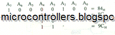
The Z80 microprocessor has several output instructions to send (copy or write) data to an output device. It can send data from the accumulator, internal general purpose registers, or memory registers to an output device. The Out instructions include the 8-bit address of a device as an operand. Therefore, the address can be any of the 256 8-bit binary combinations from OOH to FFH• Thus, an output device can be assigned any 8-bit address between OOH and FFH through an appropriate interfacing circuit. The address range from OOH to FFH is called the I/O or periph­eral map, and an address can be referred to as a device address, port address, or port number. Among the several Out instructions, we will examine the machine cycles and timing of the following instruction.

Untitled-3_03

This is a 2-byte instruction with the hexadecimal opcode D3, and the second byte is the port ad­dress of an output device.

This instruction transfers (copies) data from the accumulator to the output device.

Typically, to display the contents of the accumulator at an output device (such as LEDs) with the address, for example, 07H, the instruction will be written and stored in memory as follows:

When the microprocessor reads and executes the machine codes written at memory registers 2050H and 2051H, it will transfer (copy) the byte from the accu­mulator to the LED port with address 07H and display the byte. Now the question remains: How is the address 07H assigned to the output port? To answer that question, we need to examine the machine cycles of this instruction, as shown in the next section.

5.1.2 Execution of OUT Instruction and Timing

The OUT instruction has three machine cycles: Opcode Fetch, Memory Read, and I/O Write. The Z80 reads the opcode and the port address from memory in the first two machine cycles and writes into the port in the third cycle. Figure 5.1 shows the timing of the OUT instruction with the port address 07H

The first two machine cycles-Opcode Fetch and Memory Read-are simi­lar to the machine cycles shown in Figure 3.5; however, in Figure 5.1, the low order and high-order address buses are shown separately to illustrate the contents of the low-order bus in the third cycle. In the Opcode Fetch cycle, the Z80 places the address 2050H on the address bus and fetches the opcode D3H (1 1 0 I 00 1 1) via the data bus. When the Z80 decodes the opcode, it realizes that the instruction consists of two bytes, and that it must read the second byte. In the second ma­chine cycle, the Z80 places the next address, 2051H, on the address bus and reads the port address 07H

In the third machine ‘cycle, M3 (I/O Write), the following events occur:

1. The Z80 places the port address 07 H on the low-order address bus and the contents of the accumulator on the data bus.

Untitled-4


2. During T2, it asserts the I͞͞O͞R͞Q͞ and ͞͞͞͞W͞͞R͞ control signals; the assertion of I͞͞O͞R͞Q͞ indicates that it is an I/O operation.

3. The Z80 automatically inserts a single Wait state Tw after T2 to allow sufficient response time for an I/O device; this Wait state is added regardless of the WAIT signal status.

4. During T3, the control signals I͞͞O͞R͞Q͞ and W͞͞R͞ become inactive.

To interface an output device, the information on the buses during the M3 cycle is critical. From the beginning of T2 until the end of T3, we have the port address (07H) on the low-order address bus and the data byte to be displayed on the data bus. The availability of this information is indicated by the control sig­nals. Now what we must do is to latch (catch) this information using the control signals before it disappears from the buses; we need to open the gate at that precise moment to let the data flow to the "outside world." This is the essence of interfacing.


ASSIGNMENTS ON MEMORY INTERFACING

1. if a memory chip is organized in a 4096 x 1 format, specify the number of registers in the chip and the number of bits stored by each register.

2. if 16K x 1 memory chips are used in a memory design, how many chips are required to design 64K-byte memory?

3. Specify the number of chips necessary to design 8K-byte memory with 1024 x 4 memory chips.

4. In Figure 1 . generate the equivalent M͞S͞EL0 " signal by using a4-input NAND gate (and inverters) to decode the address lines A15-A13 and the M͞R͞E͞Q.

5. Generate the signal equivalent to the M͞S͞E͞L0 signal in Figure 7 using the 74LS139. which bas two 2-to-4 decoders in the package.

6. In Figure 7. if we use connect the output line O5 , (instead of O0 ) of the decoder to the C͞E signal, what will be the memory address range or the circuit?

7. In Figure 7. if we use all the output lines (O7-O0) or the decoder to select memory chips of the same size as the 2764 , what is the total range of the memory map ?

8. If the first address of the 8K x 8 memory chip is 4000H , what is the address of the last register ?

9. In Figure 9. replace the address line A15 , with A11 and find the range of the foldback memory.

10. In Figure 9. replace the address lines A15 and A14 by A12 and A11 Find the range of foldback memory.

11. By examining the range of the foldback memory in Figure 9, specify the relationship between the range of foldback memory and the number of "don"t care" lines.

12. In Figure 12. the control signals R͞D, M͞R͞E͞Q and W͞R are used as inputs to the 3-to-8 decoder, and the decoder is enabled. Specify the output lines that can be used as M͞E͞M͞RD and M͞E͞M͞W͞R control signals.

13. In Figure 12. explain why the output line O0. cannot be asserted low.

14. In Figure 13. specify the memory maps of ROM 1, ROM2. and R/WM1.

15. is there a foldback memory for any one of the chips in Figure 13?

16. Sketch the memory map in Figure 13.

17. Given a 1K (1024 x 8) EPROM memory chip and one 3-to-8 decoder, de­sign an interfacing circuit to assign the beginning address at Use the 74LS32 OR gate to generate the control signal M͞E͞M͞RD.

18. You are given the 74LS139 (two 2-to-4 decoders) and 8K static: R/W mem­ory. Use one decoder to assign the starting memory address at 8000H . and

FIGOREU 12

Generating Control Signals Using the 3-to-8 Decoder

microproccessor-architecture&memory-interfacing-24_03

FIGURE 4.13

Schematic for Assignments 14-16

microproccessor-architecture&memory-interfacing-45_03

use the other decoder to generate the M͞E͞M͞RD and M͞E͞M͞W͞R control signals.

The following questions refer to section 5 and Figure 10.

19. If the diagnostic routine is executed on a system with the clock frequency 4 MHz, specify the time interval between two W͞R pulses.

20. In the diagnostic routine, how many times is the M͞R͞E͞Q signal asserted in one loop?

21. Specify the logic levels of the address lines A15 and A13 and the data lines D7 and D3 .when the W͞R signal is asserted during the diagnostic routine.

22. How many times is the M͞1 signal asserted during the execution of the diag­nostic routine?

23. How many times is M͞S͞E͞L1asserted in one loop.


SUMMARY OF MEMORY INTERFACING


MEMORY INTERFACING

  • To read from memory, the address of the register to be read from should be placed on the address lines; arid the Chip Enable C͞E and R͞D signals must be , asserted low to enable the Output buffer.
  • To write into memory, die address of the register to be written into should be placed on the address lines; a data byte should be placed on the data lines, and the Chip Enable C͞E and W͞R signals must be asserted low to enable the input buffer.
  • The Z80 identifies memory operations by initiating the M͞R͞E͞Q signal. This signal is combined with the decoded address pulse (C͞S) generate Memory Select (M͞S͞EL), which is connected to the Chip Enable (C͞E) signal of the memory chip. Another alternative is to use the decoded address pulse C͞S to enable the memory chip and generate Memory Read (M͞E͞M͞R͞D) and Memory Write (M͞E͞M͞W͞R) signals by combining M͞R͞E͞Q , R͞D, and W͞R signals.
  • To interface a memory chip with the Z80, the necessary low-order address lines of the Z80 address bus are connected to the address lines Of the memory chip. The high-order address lines and the M͞R͞E͞Q are used to generate to M͞S͞EL signal, which enables the chip. The R͞D signal is used to enable the output buffer and the W͞R signal is used to write into memory by enabling the input buffer .
  • In the absolute decoding technique, all the address lines not used by a mem­ory chip to identify a memory register must be decoded; thus, die Chip Select can be asserted by only one address. In the partial decoding technique, some address lines can be left as ”’don’t care. " This technique saves on hardware. Out generates multiple addresses, which result in foldback memory space.
  • To troubleshoot an interfacing circuit, a constant and identifiable signal must be generated by writing a continuous loop.
 

SOME QUESTIONS AND ANSWERS ON MEMORY INTERFACING

In the above discussion of memory interfacing, we focused on certain aspects of the communication process between the Z80 and memory. However, in order to avoid distraction from basic concepts, we did not address several important is­sues. Now we will attempt to answer those questions briefly or provide references for them : . .

index

  1. How do you determine whether a memory chip is too slow for a given Z80 system?

The response time of a memory chip is defined in terms of Access Time.

This is the time delay between when the microprocessor places a memory address on the address bus and when memory places a data byte on the data bus. Typi­cally, Access Time is 50-450 ns for static RIW memory. Similarly, the micropro­cessor has a timing specification: the time delay after the Z80 places an address on the address bus to When it begins to read data on the data bus. The memory access time must be less than this microprocessor time delay. This will be dis. cussed when we consider advanced topics in memory interfacing .

2 . How do you interface a memory chip with slow response time?

If the memory response time is slower than the microprocessor read time, the Memory Read cycle can be extended by using the WAIT signal. During the T, state of the Memory Read cycle, the Z80 samples the WAIT signal, and if it is row, the Z80 adds Wait states until the signal goes high again. Typically, one Wait state (one clock cycle) provides sufficient time for memory to place data on the data bus. Extra circuitry is necessary for adding Wait states; this is discussed in topic 16.

3. Why did you omit an illustrative example of dynamic memory?

The dynamic memory stores information as a capacitive charge; therefore, information needs to be refreshed every few milliseconds. In the latter part of the Opcode Fetch cycle, the Z80 uses the low-order bus for refresh addresses. To interface the dynamic memory, additional refresh circuits that can use the refresh addresses from the Opcode Fetch cycle are necessary. This will also be discussed in topic 16.


TESTING AND TROUBLESHOOTING INTERFACING CIRCUITS

In the last section, we discussed how to design or interface .memory for a given address. The next step is to test and verify that we can store a byte at a memory location within the address range of the memory chip and read the byte. At this point, we need to make an assumption that we have a working microcomputer system, and the memory design is an expansion of the existing system. If we are designing a system, we may need to use an in-circuit emulator to test the memory; this is discussed in Topic 17.

To test the memory, We can simply access an address such as 2800H through the system keyboard, store a byte, and check the address location again to verify the byte. If there is any fault in the interfacing circuit, ‘the system is likely to show an error message, or a different byte from the one we stored will be displayed. Now we need to troubleshoot the interfacing circuit. The question is: Where do we begin? The obvious step is to check the wiring and the pin connections After this preliminary check, most traditional methods used in checking analog circuits (such as an amplifier) are ineffective because the logic levels on the buses are dynamic; they constantly change depending upon the operation being performed at a given instant by the microprocessor. In troubleshooting analog circuits, a commonly used technique is signal injection, whereby a known signal is injected at the input, and the output signal is verified against the expected outcome; To use this concept, we need to generate a constant and identifiable signal and check various points in relation to that signal. We can generate such a signal by asking the processor to execute a continuous loop, called a diagnostic routine, as shown.

START:     LD A, F7H                          ;Load F7H into the accumulator

                  LD (2800H), A                  ;Store accumulator contents in

                                                             ; location 2800H

                  JP START                          ;Jump back to beginning and repeat

This routine has three instructions. The first instruction loads F7H into the accumulator (the byte F7H is selected arbitrarily), and the second instruction stores the byte in the memory location 2800H. The third instruction is a Jump instruction that takes the program control at the beginning, and these three in­structions are repeated continuously. Now we need to examine the machine cycles of these instructions to find an identifiable signal that is repeated at a certain interval. We can analyze the loop in the machine cycles as follows (it will be helpful to have read Topic 6 to understand the diagnostic routine):

Untitled-41-22

This loop has 30 T-states and nine operations. To execute the loop once. the microprocessor asserts the R͞D signal eight times (the Opcode Fetch is also a Read operation) and the W͞R signal once. Assuming the system clock frequency is 2 MHz. the loop is executed in 15 µs, and the W͞R signal, repeated every 15 µs, can be observed on a scope. If we sync the scope on the W͞R pulse from the Z80,

Untitled-41-2-2

FIGURE 11

Timing Signals of Diagnostic Routine

MEMORY INTERFACING

we can check M͞1 the output of the decoder M͞S͞EL, and memory signals C͞E, W͞R, and R͞D; three of these signals are in Figure 11.

When the Z80 asserts the W͞R signal, the high-order address A15-A11 must be 0 0 1 0 1, and M͞S͞E͞L, must be asserted low. If M͞S͞E͞L , is high, it indicates that the address lines A15-A11 or M͞R͞E͞Q are improperly connected or the decoder chip is faulty.

if M͞S͞EL, is low, it confirms that the decoding circuit is functioning properly .

Now if we check the entire address bus and the data bus in relation to the W͞R signal, one line at a time, we must read the address 2800H and the data F7H if we check the R͞D signal, it must be high when the W͞R is -asserted, and we will observe eight R͞D signals between every two W͞R signals, as shown in Figure 11.


ILLUSTRATIVE EXAMPLE 2: INTERFACING STATIC RIW MEMORY

In this example, we will use the MOSTEK MK4802 memory chip to demonstrate both Read and Write operations. To simplify the discussion, we will use the same decoding circuit as in Figure 7, except the M͞S͞E͞L4 signal is used as the Chip Enable. This chip has 2K of memory; therefore, two address lines (A12 and All) have to be left as "don’t care" to use the previous circuit. Because of the "don’t care" address line, the memory registers will have multiple addresses, and the memory chip will occupy more memory space than necessary (explained later).

MOSTEK MK4802 Static R/W Memory

This is a 2K static R/W memory chip, organized as 2048 x 8 format. It has eleven address lines (A10-A0), eight data lines, and three control signals: C͞E, O͞E: and W͞E. We are already familiar with the first two control signals, and the third signal

microproccessor-architecture&memory-interfacing-37_03

FIGURE 4.8

MK4802 or CMOS 6116 Static R/W Memory Pin Configuration and Logic Symbol


W͞E (Write Enable), is active low and used to enable the input buffer of the mem­ory. The logic pinout and the pin configuration are shown in Figure 8.

Interfacing Circuit

Figure 9 shows the interfacing circuit using the MK4802 memory chip. The de­coding circuit is the same as in Figure 7. We will analyze this circuit in terms of the same three steps outlined previously.

Step 1: The Z80 address lines A10-A0 are connected to pins A10-A0 of the mem­ory chip to address 2048 registers. The address lines A12 and A11 can be used by using a different decoder, but we have left these lines as "don’t care" to observe its effects on the memory map. Furthermore. this is a commonly used industrial practice for small microprocessor-based systems .

Untitled-38-222222222

FIGURE 9

Schematic of Interfacing Static R/W Memory MK4802

Step 2 The Memory Select M͞S͞EL4 line, the output O4 of the decoder, is used as

& the Chip Enable (C͞E). The C͞E is asserted only when the address on A15

Step 3: A13 is 1 0 0 .

Step 4:

In case of an R/W memory, we need two control signals: Read (R͞D) and Write (W͞R), both active low. The R͞D is connected to O͞E, as in the pre­vious illustration, to enable the output buffer. The WR is connected to W͞E (Write Enable) of the memory chip. and when W͞R is asserted low, the input buffer of the memory chip is enabled, allowing data to be writ­ten into a memory register.

Memory Map

Assuming the "don’t care" address lines A12 and A11 are at logic 0 , the first memory address range is from 4000H to 47FFH as shown below:

microproccessor-architecture&memory-interfacing-38_07

Now, to examine the other addresses of this memory chip, we need to con­sider the remaining combinations of the address lines A12 and A11 . These two lines can have four combinations (00, 01, 10, 11). The first combination is already used, and the remaining three combinations will give us the following address ranges.

microproccessor-architecture&memory-interfacing-38-_03

The entire-memory map appears to be from 8000H to 9FFFH; 8K of memory.

Actually, we have only 8K of memory occupying the memory space of 8K. Be­cause of the two "don’t care" lines, each register can have four addresses. For example, the addresses 8000H, 8800H, 9000H, and 9800H will select the same reg­ister. By convention, the first set of the address (8000H-87FFH) is considered as the basic memory address range. The remaining duplicate ranges of the memory addresses (8800H to 9FFFH) are generally known as the foldback memory; this memory space cannot be used by any other memory chip. The foldback memory is the result of the partial decoding practices (having "don’t care" lines). This is a common practice in microprocessor-based products where memory size is small. Even if such a practice wastes some memory space of the 64K memory map, it reduces the chip count on a board.