In the last section, we discussed how to design or interface .memory for a given address. The next step is to test and verify that we can store a byte at a memory location within the address range of the memory chip and read the byte. At this point, we need to make an assumption that we have a working microcomputer system, and the memory design is an expansion of the existing system. If we are designing a system, we may need to use an in-circuit emulator to test the memory; this is discussed in Topic 17.
To test the memory, We can simply access an address such as 2800H through the system keyboard, store a byte, and check the address location again to verify the byte. If there is any fault in the interfacing circuit, ‘the system is likely to show an error message, or a different byte from the one we stored will be displayed. Now we need to troubleshoot the interfacing circuit. The question is: Where do we begin? The obvious step is to check the wiring and the pin connections After this preliminary check, most traditional methods used in checking analog circuits (such as an amplifier) are ineffective because the logic levels on the buses are dynamic; they constantly change depending upon the operation being performed at a given instant by the microprocessor. In troubleshooting analog circuits, a commonly used technique is signal injection, whereby a known signal is injected at the input, and the output signal is verified against the expected outcome; To use this concept, we need to generate a constant and identifiable signal and check various points in relation to that signal. We can generate such a signal by asking the processor to execute a continuous loop, called a diagnostic routine, as shown.
START: LD A, F7H ;Load F7H into the accumulator
LD (2800H), A ;Store accumulator contents in
; location 2800H
JP START ;Jump back to beginning and repeat
This routine has three instructions. The first instruction loads F7H into the accumulator (the byte F7H is selected arbitrarily), and the second instruction stores the byte in the memory location 2800H. The third instruction is a Jump instruction that takes the program control at the beginning, and these three instructions are repeated continuously. Now we need to examine the machine cycles of these instructions to find an identifiable signal that is repeated at a certain interval. We can analyze the loop in the machine cycles as follows (it will be helpful to have read Topic 6 to understand the diagnostic routine):
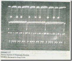
This loop has 30 T-states and nine operations. To execute the loop once. the microprocessor asserts the R͞D signal eight times (the Opcode Fetch is also a Read operation) and the W͞R signal once. Assuming the system clock frequency is 2 MHz. the loop is executed in 15 µs, and the W͞R signal, repeated every 15 µs, can be observed on a scope. If we sync the scope on the W͞R pulse from the Z80,
FIGURE 11
Timing Signals of Diagnostic Routine
MEMORY INTERFACING
we can check M͞1 the output of the decoder M͞S͞EL, and memory signals C͞E, W͞R, and R͞D; three of these signals are in Figure 11.
When the Z80 asserts the W͞R signal, the high-order address A15-A11 must be 0 0 1 0 1, and M͞S͞E͞L, must be asserted low. If M͞S͞E͞L , is high, it indicates that the address lines A15-A11 or M͞R͞E͞Q are improperly connected or the decoder chip is faulty.
if M͞S͞EL, is low, it confirms that the decoding circuit is functioning properly .
Now if we check the entire address bus and the data bus in relation to the W͞R signal, one line at a time, we must read the address 2800H and the data F7H if we check the R͞D signal, it must be high when the W͞R is -asserted, and we will observe eight R͞D signals between every two W͞R signals, as shown in Figure 11.

