ILLUSTRATIVE EXAMPLE 2:
INTERFACING INPUT SWITCHES
In this section, we will analyze the circuit used for interfacing eight DIP switches as shown in Figure 5.8. The circuit includes the 74LS138 3-to-8 decoder to decode the low-order bus and the tri-state octal buffer (74LS244) to interface the switches to the data bus. The port can be accessed with the address 84H; however, it also has multiple addresses.

5.4.1 Hardware
Figure 5.8 shows the 74LS244 tri-state octal buffer used as an interfacing device. The device has two groups of four buffers each, and they are controlled by the active low signal O̅E̅ .When O̅E̅ is low, the input data appear on the output lines, and when O̅E̅ is high, the output lines assume high impedance state.
5.4.2 Interfacing Circuit
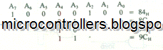
Figure 5.8 shows that the low-order address bus (with the exception of lines A4 and A3) is connected to the decoder 74LS138; the address lines A4 and A3 are left in the “don’t care” state. The output line 04 of the decoder goes low when the address bus has the following address (we assume the “don’t care” lines are at logic O):

The control signal I/Q Read (I̅O̅R̅D̅)is generated by ANDing the I͞͞O͞R͞Q͞ and R̅D̅ in a negative NAND gate, and the I/O select pulse is generated by ANDing the output of the decoder with the control signal I̅O̅R̅D̅. When the address is 84H and the control signals I͞͞O͞R͞Q͞ and R̅D̅ are asserted, the I/O select pulse enables, the I/O select pulse enables the tri-state buffer, and the logic levels of the switches are placed on the data bus. The Z80 then reads switch positions during T3 (Figure 5.7) and places the data byte into the accumulator. When a switch is closed, it has logic 0, and when it is open, it is tied to + 5 V, representing logic 1. Figure 5.8 shows that the switches S7-S3 are open and S2-S0 are closed; thus, the input reading will be F8H•
5.4.3 Multiple Port Addresses
In Figure 5.8, the address lines A4 and A3 are not used by the decoding circuit; the logic levels on these lines can be either 0 or 1. Therefore, this input port can be accessed by four different addresses, as shown.
5.4.4 Instructions to Read Input Port
To read data from the input port shown in Figure 5.8, the instruction IN A, (84H) can be used. When this instruction is executed, the Z80 places the address 84H on the low-order bus, asserts the control signals, and reads the switch positions.