1. if a memory chip is organized in a 4096 x 1 format, specify the number of registers in the chip and the number of bits stored by each register.
2. if 16K x 1 memory chips are used in a memory design, how many chips are required to design 64K-byte memory?
3. Specify the number of chips necessary to design 8K-byte memory with 1024 x 4 memory chips.
4. In Figure 1 . generate the equivalent M͞S͞EL0 " signal by using a4-input NAND gate (and inverters) to decode the address lines A15-A13 and the M͞R͞E͞Q.
5. Generate the signal equivalent to the M͞S͞E͞L0 signal in Figure 7 using the 74LS139. which bas two 2-to-4 decoders in the package.
6. In Figure 7. if we use connect the output line O5 , (instead of O0 ) of the decoder to the C͞E signal, what will be the memory address range or the circuit?
7. In Figure 7. if we use all the output lines (O7-O0) or the decoder to select memory chips of the same size as the 2764 , what is the total range of the memory map ?
8. If the first address of the 8K x 8 memory chip is 4000H , what is the address of the last register ?
9. In Figure 9. replace the address line A15 , with A11 and find the range of the foldback memory.
10. In Figure 9. replace the address lines A15 and A14 by A12 and A11 Find the range of foldback memory.
11. By examining the range of the foldback memory in Figure 9, specify the relationship between the range of foldback memory and the number of "don"t care" lines.
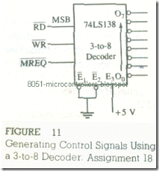
12. In Figure 12. the control signals R͞D, M͞R͞E͞Q and W͞R are used as inputs to the 3-to-8 decoder, and the decoder is enabled. Specify the output lines that can be used as M͞E͞M͞RD and M͞E͞M͞W͞R control signals.
13. In Figure 12. explain why the output line O0. cannot be asserted low.
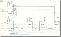
14. In Figure 13. specify the memory maps of ROM 1, ROM2. and R/WM1.
15. is there a foldback memory for any one of the chips in Figure 13?
16. Sketch the memory map in Figure 13.
17. Given a 1K (1024 x 8) EPROM memory chip and one 3-to-8 decoder, design an interfacing circuit to assign the beginning address at Use the 74LS32 OR gate to generate the control signal M͞E͞M͞RD.
18. You are given the 74LS139 (two 2-to-4 decoders) and 8K static: R/W memory. Use one decoder to assign the starting memory address at 8000H . and
FIGOREU 12
Generating Control Signals Using the 3-to-8 Decoder
FIGURE 4.13
Schematic for Assignments 14-16
use the other decoder to generate the M͞E͞M͞RD and M͞E͞M͞W͞R control signals.
The following questions refer to section 5 and Figure 10.
19. If the diagnostic routine is executed on a system with the clock frequency 4 MHz, specify the time interval between two W͞R pulses.
20. In the diagnostic routine, how many times is the M͞R͞E͞Q signal asserted in one loop?
21. Specify the logic levels of the address lines A15 and A13 and the data lines D7 and D3 .when the W͞R signal is asserted during the diagnostic routine.
22. How many times is the M͞1 signal asserted during the execution of the diagnostic routine?
23. How many times is M͞S͞E͞L1asserted in one loop.

