In this example, we will use the MOSTEK MK4802 memory chip to demonstrate both Read and Write operations. To simplify the discussion, we will use the same decoding circuit as in Figure 7, except the M͞S͞E͞L4 signal is used as the Chip Enable. This chip has 2K of memory; therefore, two address lines (A12 and All) have to be left as "don’t care" to use the previous circuit. Because of the "don’t care" address line, the memory registers will have multiple addresses, and the memory chip will occupy more memory space than necessary (explained later).
MOSTEK MK4802 Static R/W Memory
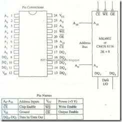
This is a 2K static R/W memory chip, organized as 2048 x 8 format. It has eleven address lines (A10-A0), eight data lines, and three control signals: C͞E, O͞E: and W͞E. We are already familiar with the first two control signals, and the third signal
FIGURE 4.8
MK4802 or CMOS 6116 Static R/W Memory Pin Configuration and Logic Symbol
W͞E (Write Enable), is active low and used to enable the input buffer of the memory. The logic pinout and the pin configuration are shown in Figure 8.
Interfacing Circuit
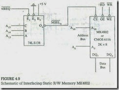
Figure 9 shows the interfacing circuit using the MK4802 memory chip. The decoding circuit is the same as in Figure 7. We will analyze this circuit in terms of the same three steps outlined previously.
Step 1: The Z80 address lines A10-A0 are connected to pins A10-A0 of the memory chip to address 2048 registers. The address lines A12 and A11 can be used by using a different decoder, but we have left these lines as "don’t care" to observe its effects on the memory map. Furthermore. this is a commonly used industrial practice for small microprocessor-based systems .
FIGURE 9
Schematic of Interfacing Static R/W Memory MK4802
Step 2 The Memory Select M͞S͞EL4 line, the output O4 of the decoder, is used as
& the Chip Enable (C͞E). The C͞E is asserted only when the address on A15–
Step 3: A13 is 1 0 0 .
Step 4:
In case of an R/W memory, we need two control signals: Read (R͞D) and Write (W͞R), both active low. The R͞D is connected to O͞E, as in the previous illustration, to enable the output buffer. The WR is connected to W͞E (Write Enable) of the memory chip. and when W͞R is asserted low, the input buffer of the memory chip is enabled, allowing data to be written into a memory register.
Memory Map
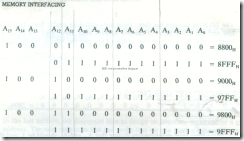
Assuming the "don’t care" address lines A12 and A11 are at logic 0 , the first memory address range is from 4000H to 47FFH as shown below:
Now, to examine the other addresses of this memory chip, we need to consider the remaining combinations of the address lines A12 and A11 . These two lines can have four combinations (00, 01, 10, 11). The first combination is already used, and the remaining three combinations will give us the following address ranges.
The entire-memory map appears to be from 8000H to 9FFFH; 8K of memory.
Actually, we have only 8K of memory occupying the memory space of 8K. Because of the two "don’t care" lines, each register can have four addresses. For example, the addresses 8000H, 8800H, 9000H, and 9800H will select the same register. By convention, the first set of the address (8000H-87FFH) is considered as the basic memory address range. The remaining duplicate ranges of the memory addresses (8800H to 9FFFH) are generally known as the foldback memory; this memory space cannot be used by any other memory chip. The foldback memory is the result of the partial decoding practices (having "don’t care" lines). This is a common practice in microprocessor-based products where memory size is small. Even if such a practice wastes some memory space of the 64K memory map, it reduces the chip count on a board.


