Data Storage Systems : Introduction , Redundant Arrays of Independent Disks (RAID) Systems RAID Elements and RAID Levels

Data Storage Systems

Introduction

The astounding volume of data being transmitted between systems today has created an obvious need for data management. As a result, more servers—whether they are PCs, UNIX workstations, minicomputers, or supercomputers—have assumed the role of information providers and managers. The number of networked or connectable systems is increasing by leaps and bounds as well, thanks to the widespread adoption of the client-server computing model. Hard disk storage plays an important role in enabling improvements to networked systems, because the vast and growing ocean of data needs to reside some- where. It also has to be readily accessible, placing a demand upon storage system manufacturers to not only provide high-capacity products, but products that can access data as fast as possible and to as many people at the same time as possible. Such storage also needs to be secure, placing an importance on reliability features that best ensure data will never be lost or otherwise rendered inaccessible to network system users.

Redundant Arrays of Independent Disks (RAID) Systems

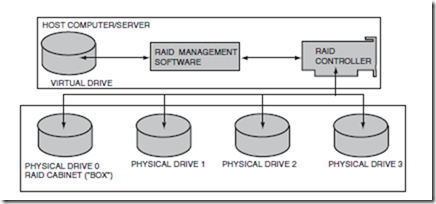
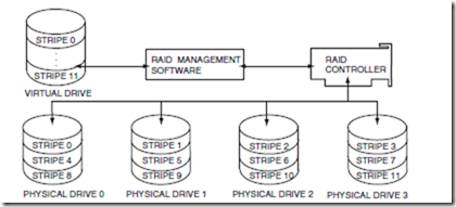
The common solution to providing access to many gigabytes of data to users fast and reliably has been to assemble a number of drives together in a gang or array of disks, known as redundant arrays of independent disks (RAID) subsystems. Simple RAID subsystems are basically a cluster of up to five or six disk drives assembled in a cabinet that are all connected to a single controller board. The RAID controller orchestrates read and write activities in the same way a controller for a single disk drive does, and treats the array as if it were in fact a single or virtual drive. RAID management software that resides in the host system provides the means to manage data to be stored on the RAID subsystem. A typical RAID configuration is illustrated in Fig. 24.1.

RAID Elements

Despite its multidrive configuration, the individual disk drives of a RAID subsystem remain hidden from users; the subsystem itself is the virtual drive, though it can be infinitely large. The phantom virtual drive is created at a lower level within the host operating system through the RAID management software. Not only does the software set up the system to address the RAID unit as if it were a single drive, it allows the subsystem to be configured in ways that best suit the general needs of the host system.

RAID subsystems can be optimized for performance, highest capacity, fault tolerance, or a combination of these attributes. Different RAID levels have been defined and standardized in accordance with these

image

FIGURE 24.1 A typical RAID configuration. (Source: Adapted from Heyn, T. 1995. The RAID Advantage. Seagate Technology Paper, Seagate, Scotts Valley, CA.)

general optimization parameters. There are six such standardized levels RAID, called RAID 0, 1, 2, 3, 4, and 5, depending on performance, redundancy and other attributes required by the host system.

The RAID controller board is the hardware element that serves as the backbone for the array of disks; it not only relays the input/output (I/O) commands to specific drives in the array, but provides the physical link to each of the independent drives so that they may easily be removed or replaced. The controller also serves to monitor the integrity of each drive in the array to anticipate the need to move data should it be placed in jeopardy by a faulty or failing disk drive (a feature known as fault tolerance).

RAID Levels

The RAID 0–5 standards offer users and system administrators a host of configuration options. These options permit the arrays to be tailored to their application environments. Each of the various configurations focus on maximizing the abilities of an array in one or more of the following areas:

  • Capacity
  • Data availability
  • Performance
  • Fault tolerance
RAID Level 0

An array configured to RAID level 0 is an array optimized for performance, but at the expense of fault tolerance or data integrity. RAID level 0 is achieved through a method known as striping. The collection of drives (virtual drive) in a RAID level 0 array has data laid down in such a way that it is organized in stripes across the multiple drives. A typical array can contain any number of stripes, usually in multiples of the number of drives present in the array. Take, as an example, a four-drive array configured with 12 stripes (four stripes of designated space per drive). Stripes 0, 1, 2, and 3 would be located on corresponding hard drives 0, 1, 2, and 3. Stripe 4, however, appears on a segment of drive 0 in a different location than stripe 0; stripes 5–7 appear accordingly on drives 1, 2, and 3. The remaining four stripes are allocated in the same even fashion across the same drives such that data would be organized in the manner depicted in Fig. 24.2. Practically any number of stripes can be created on a given RAID subsystem for any number of drives: 200 stripes on two disk drives is just as feasible as 50 stripes across 50 hard drives. Most RAID subsystems, however, tend to have between 3 and 10 stripes.

The reason RAID 0 is a performance-enhancing configuration is that striping enables the array to access data from multiple drives at the same time. In other words, because the data is spread out across a number of drives in the array, it can be accessed faster because it is not bottled up on a single drive. This is especially beneficial for retrieving a very large file, because it can be spread out effectively across multiple drives and accessed as if it were the size of any of the fragments it is organized into on the data stripes.

image

FIGURE 24.2 In a RAID level 0 configuration, a virtual drive comprises several stripes of information. Each consecutive stripe is located on the next drive in the chain, evenly distributed over the number of drives in the array. (Source: Adapted from Heyn, T. 1995. The RAID Advantage. Seagate Technology Paper, Seagate, Scotts Valley, CA.)

The downside to RAID level 0 configurations is that it sacrifices fault tolerance, raising the risk of data loss because no room is made available to store redundant data. If one of the drives in the RAID 0 fails for any reason, there is no way of retrieving the lost data, as can be done in other RAID implementations.

RAID Level 1

The RAID level 1 configuration employs what is known as disk mirroring, which is done to ensure data reliability or a high degree of fault tolerance. RAID 1 also enhances read performance, but the improved performance and fault tolerance come at the expense of available capacity in the drives used. In a RAID level 1 configuration, the RAID management software instructs the subsystem’s controller to store data redundantly across a number of the drives (mirrored set) in the array. In other words, the same data is copied and stored on different disks to ensure that, should a drive fail, the data is available somewhere else within the array. In fact, all but one of the drives in a mirrored set could fail and the data stored to the RAID 1 subsystem would remain intact. A RAID level 1 configuration can consist of multiple mirrored sets, whereby each mirrored set can be a different capacity. Usually the drives making up a mirrored set are of the same capacity. If drives within a mirrored set are of different capacities, the capacity of a mirrored set within the RAID 1 subsystem is limited to the capacity of the smallest capacity drive in the set, hence the sacrifice of available capacity across multiple drives.

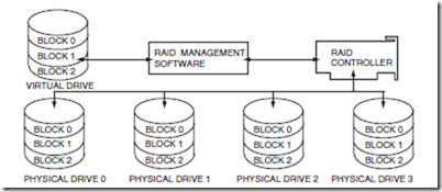
The read performance gain can be realized if the redundant data is distributed evenly on all of the drives of a mirrored set within the subsystem. The number of read requests and total wait state times both drop significantly, inversely proportional to the number of hard drives in the RAID, in fact. To illustrate, suppose three read requests are made to the RAID level 1 subsystem (see Fig. 24.3). The first request looks for data in the first block of the virtual drive; the second request goes to block 0, and the third seeks from block 2. The host-resident RAID management software can assign each read request to an individual drive. Each request is then sent to the various drives, and now—rather than having to handle the flow of each data stream one at a time—the controller can send three data streams almost simultaneously, which in turn reduces system overhead.

RAID Level 2

RAID level 2 is rarely used in commercial applications, but is another means of ensuring data is protected in the event drives in the subsystem incur problems or otherwise fail. This level builds fault tolerance around Hamming error correction code (ECC), which is often used in modems and solid-state memory devices as a means of maintaining data integrity. ECC tabulates the numerical values of data stored on specific blocks in the virtual drive using a formula that yields a checksum. The checksum is then appended to the end of the data block for verification of data integrity when needed.

image

FIGURE 24.3 A RAID level 1 subsystem provides high data reliability by replicating (mirroring) data between physical hard drives. In addition, I/O performance is boosted as the RAID management software allocates simultaneous read requests between several drives. (Source: Adapted from Heyn, T. 1995. The RAID Advantage. Seagate Technology Paper, Seagate, Scotts Valley, CA.)

As data is read back from the drive, ECC tabulations are again computed, and specific data block checksums are read and compared against the most recent tabulations. If the numbers match, the data is intact; if there is a discrepancy, the lost data can be recalculated using the first or earlier checksum as a reference point, as illustrated in Table 24.1.

This form of ECC is actually different from the ECC technologies employed within the drives themselves. The topological formats for storing data in a RAID level 2 array is somewhat limited, however, compared to the capabilities of other RAID implementations, which is why it is not commonly used in commercial applications.

RAID Level 3

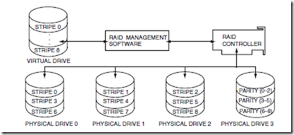
This RAID level is essentially an adaptation of RAID level 0 that sacrifices some capacity, for the same number of drives, but achieves a high level of data integrity or fault tolerance. It takes advantage of RAID level 0 data striping methods, except that data is striped across all but one of the drives in the array. This drive is used to store parity information for maintenance of data integrity across all drives in the subsystem. The parity drive itself is divided into stripes, and each parity drive stripe is used to store parity information for the corresponding data stripes dispersed throughout the array. This method achieves high data transfer performance by reading from or writing to all of the drives in parallel or simultaneously but retains the means to reconstruct data if a given drive fails, maintaining data integrity for the system. This concept is illustrated in Fig. 24.4. RAID level 3 is an excellent configuration for moving very large sequential files in a timely manner. The stripes of parity information stored on the dedicated drive are calculated using the Exclusive OR function. By using Exclusive OR with a series of data stripes in the RAID, any lost data can easily be recovered. Should a drive in the array fail, the missing information can be determined in a manner similar to solving for a single variable in an equation.

image

clip_image006

image

FIGURE 24.4 A RAID level 3 configuration is similar to a RAID level 0 in its utilization of data stripes dispersed over a series of hard drives to store data. In addition to these data stripes, a specific drive is configured to hold parity information for the purpose of maintaining data integrity throughout the RAID subsystem. (Source: Adapted from Heyn, T. 1995. The RAID Advantage. Seagate Technology Paper, Seagate, Scotts Valley, CA.)

RAID Level 4

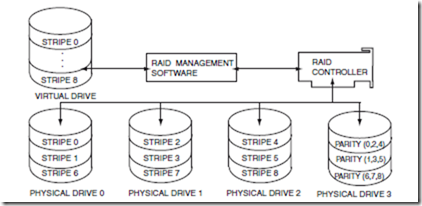
This level of RAID is similar in concept to RAID level 3, but emphasizes performance for different applications, e.g., database files vs large sequential files. Another difference between the two is that RAID level 4 has a larger stripe depth, usually of two blocks, which allows the RAID management software to operate the disks more independently than RAID level 3 (which controls the disks in unison). This essentially replaces the high data throughput capability of RAID level 3 with faster data access in read-intensive applications. (See Fig. 24.5.)

A shortcoming of RAID level 4 is rooted in an inherent bottleneck on the parity drive. As data is written to the array, the parity encoding scheme tends to be more tedious in write activities than with other RAID topologies. This more or less relegates RAID level 4 to read-intensive applications with little need for similar write performance. As a consequence, like level 3, level 4 does not see much common use in commercial applications.

RAID Level 5

This is the last of the most common RAID levels in use, and is probably the most frequently implemented. RAID level 5 minimizes the write bottlenecks of RAID level 4 by distributing parity stripes over a series of

image

FIGURE 24.5 RAID level 4 builds on RAID level 3 technology by configuring parity stripes to store data stripes in a nonconsecutive fashion. This enables independent disk management, ideal for multiple-read-intensive environments. (Source: Adapted from Heyn, T. 1995. The RAID Advantage. Seagate Technology Paper, Seagate, Scotts Valley, CA.)

image

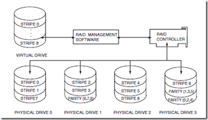
FIGURE 24.6 RAID level 5 overcomes the RAID level 4 write bottleneck by distributing parity stripes over two or more drives within the system. This better allocates write activity over the RAID drive members, thus enhancing system performance. (Source: Adapted from Heyn, T. 1995. The RAID Advantage. Seagate Technology Paper, Seagate, Scotts Valley, CA.)

hard drives. In so doing it provides relief to the concentration of write activity on a single drive, which in turn enhances overall system performance. (See Fig. 24.6.)

The way RAID level 5 reduces parity write bottlenecks is relatively simple. Instead of allowing any one drive in the array to assume the risk of a bottleneck, all of the drives in the array assume write activity responsibilities. This distribution frees up the concentration on a single drive, improving overall subsystem throughput. The RAID level 5 parity encoding scheme is the same as levels 3 and 4, and maintains the system’s ability to recover lost data should a single drive fail. This can happen as long as no parity stripe on an individual drive stores the information of a data stripe on the same drive. In other words, the parity in- formation for any data stripe must always be located on a drive other than the one on which the data resides.

Other RAID Levels

Other, less common RAID levels have been developed as custom solutions by independent vendors. Those levels include

  • RAID level 6, which emphasizes ultrahigh data integrity
  • RAID level 10, which focuses on high I/O performance and very high data integrity
  • RAID level 53, which combines RAID levels 0 and 3 for uniform read and write performance

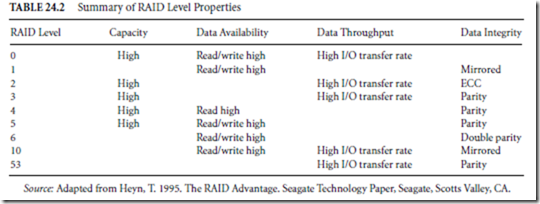
TABLE 24.2 Summary of RAID Level Properties

image

Custom RAID Systems

Perhaps the greatest advantage of RAID technology is the sheer number of possible adaptations available to users and systems designers. RAID offers the ability to customize an array subsystem to the requirements of its environment and the applications demanded of it. The inherent variety of configuration options provides several ways in which to satisfy specific application requirements, as detailed in Table 24.2. Customization, however, does not stop with a RAID level. Drive models, capacities, and performance levels have to be factored in as well as what connectivity options are available.

Defining Terms

Fiber channel-arbitrated loop (FC-AL): A high-speed interface protocol permitting high data transfer rates, large numbers of attached devices, and long-distance runs to remote devices using a combi- nation of fiber optic and copper components.

Redundant arrays of independent disks (RAID): A configuration of hard disk drives and supporting software for mass storage whose primary properties are high capacity, high speed, and reliability.

RAID level: A standardized configuration of RAID elements, the purpose of which is to achieve a given objective, such as highest reliability or greatest speed.

Single connector attachment (SCA): A cabling convention for certain interface standards that simplifies the interconnection of devices by combining data and power signals as a common, standardized port.

Small computer systems interface (SCSI): A cabling and software protocol used to interface multiple devices to a computer system. These devices may be internal and/or external to the computer itself. Several variations of SCSI exist.

Striping: A hard disk storage organization technique whereby data is stored on multiple physical devices so as to increase write and read speed.

Thermal calibration: A housekeeping function of a hard disk drive used to maintain proper alignment of the head with the disk surface.

Virtual drive: An operational state for a computing device whereby memory is organized to achieve a specific objective that usually does not exist as an actual physical entity. For example, RAM in the computer may be made to appear as a physical drive, or two or more hard disks can be made to appear as a single physical drive.

References

Anderson, D. 1995. Fiber channel-arbitrated loop: The preferred path to higher I/O performance, flexibility in design. Seagate Technology Paper No MN-24, Seagate, Scotts Valley, CA.

Heyn, T. 1995. The RAID Advantage. Seagate Technology Paper, Seagate, Scotts Valley, CA.

Tyson, H. 1995. Barracuda and elite: Disk drive storage for professional audio/video. Seagate Technology

Paper No. SV-25, Seagate, Scotts Valley, CA.

Further Information

The technology behind designing and manufacturing hard disk drives is beyond the scope of this chapter, and because most of the applied use of disks involves treating the drive as an operational component (black box, if you will), the best source of current information is usually drive manufacturers. Technical application notes and detailed product specifications are typically available at little or no cost.
 

Magnetographic and Ionographic Technologies and System Issues : Color Management

Magnetographic and Ionographic Technologies

These two technologies are toner based but utilize different addressing and writing media. The photoconductor is replaced by a thin magnetizable medium or hard dielectric layer, such as anodized aluminum, which is used in ionographic printers. Magnetographic printers employ a printhead that produces magnetic flux transitions in the magnetizable media by changing the field direction in the gap between the poles of the printhead. These magnetic transitions are sources of strong field gradient and field strength. Development is accomplished by means of magnetic toner applied via a magnetic brush. The toner parti- cles are magnetized and attracted to the medium by virtue of the strong field gradient. Transfer and fusing

proceed in a similar manner to that of electrophotography. Ionographic printers write onto a dielectric coated drum by means of a printhead containing individual electron sources. The electrons are generated in a miniature cavity by means of air breakdown under the influence of an RF field. The electron beam is focused by a screen electrode, and the cavity functions in a manner similar to that of vacuum tube valves. The role of the plate is played by the dielectric coated metal drum held at ground potential. The charge image is typically developed by monocomponent toner followed by a transfix, that is, transfer and fuse operation, often without the influence of heat. Both systems require a cleaning process: mechanical scraping for ionography and magnetic scavenging for magnetography.

System Issues

Processing and communicating data to control today’s printers raises significant system issues in view of the material to be printed. Hardcopy output may contain typography, computer-generated graphics, and natural or synthetic images in both color and black and white. The complexity of this information can require a large amount of processing, either in the host computer or in the printer itself. Applications software programs can communicate with the printer in two ways: via a page description language (PDL), or through a printer command set. The choice is driven by the scope of the printed material. If full page layout with text, graphics, and images is the goal, then PDL communication will be needed. For computer generated graphics a graphical language interface will often suffice. However, many graphics programs also provide PDL output capability. Many options exist and a careful analysis of the intended printed material is necessary to determine if a PDL interface is required.

When processing is done in the host computer, it is the function of the printer driver to convert the outline fonts, graphical objects, and images into a stream of bits to be sent to the printer. Functions that the driver may have to perform include digital halftoning, rescaling, color data transformations, and color appearance adjustments among other image processing operations, all designed to enable the printer to deliver its best print quality. Data compression in the host and decompression in the printer may be used to prevent the print speed being limited by the data rate. Printers that do their own internal data processing contain a hardware formatter board whose properties are often quoted as part of the overall specification for the printer. This is typical for printers with a PDL-based interface. Some of the advantages for this approach include speed of communication with the printer and relieving of the host computer of the processing burden, which can be significant for complex documents.

The increase in complexity of printed documents has emphasized several practical system aspects that relate to user needs: visibility and control of the printed process, font management, quick return to the software application, and printer configuration. The degree of visibility and control in the printing process depends on the choice of application and/or operating environment. Fonts, either outline or bit map, may reside on disk, on computer, or printer read-only memory (ROM). To increase speed, outline fonts in use are rasterized and stored in formatter random-access memory (RAM) or computer RAM. Worst cases exist when outline fonts are retrieved at printing and rasterization occurs on a demand basis. This can result in unacceptably slow printing. If quickness of return to the application is important, printers containing their own formatter are an obvious choice. It is necessary, therefore, to take a system view and evaluate the entire configuration (computer hardware; operating system; application program; interconnect; printer formatter, and its CPU, memory, and font storage) to determine if the user needs will be met.

The need to print color images and complex color shaded graphics has brought issues such as color matching, color appearance, and color print quality to the fore. Color printer configuration now includes choices as to halftoning algorithm, color matching method, and, in some cases, smart processing. The latter refers to customized color processing based on whether the object is a text character, image, or graphic. A further complication arises when input devices and software applications also provide some of these services, and it is possible to have color objects suffer redundant processing before being printed. This can severely degrade the print quality and emphasizes the importance of examining the entire image processing chain and turning off the redundant color processing. Color printer configuration choices focus on a tradeoff between print speed and print quality. Halftoning algorithms that minimize visible texture

and high print quality modes that require overprinting consume more processing time. For color images and graphics, the relationship between the CRT image and hard copy is a matter of choice and taste. For color graphics, it is common practice to sacrifice accuracy of the hue in the interests of colorfulness or saturation of the print. In the case of natural images, hue accuracy, particularly for flesh tones, is more important, and a different tradeoff is made. Some software and hardware vendors provide a default configuration that seeks to make the best processing choice based on a knowledge of the content to be printed. If more precise control is desired, some understanding of the color reproduction issues represented by the combination of color input and output devices linked by a PC having a color monitor is required. This is the domain of color management.

Color Management

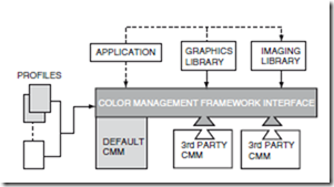
The fundamental issue to be addressed by color management is that of enabling the three broad classes of color devices (input, display, output) to communicate with each other in a system configuration. The technical issue in this is one of data representation. Each device has an internal representation of color information that is directly related to the nature in which it either represents or records that information. For printers it is typically amounts of cyan, magenta, yellow, and often black (CMY, K) ink; for displays, digital counts of red, green, and blue (RGB); and for many input devices, digitized values of RGB. These internal spaces are called device spaces and map out the volume in three-dimensional color space that can be accessed by the device. To communicate between the devices these internal spaces are converted either by analytical models or three-dimensional lookup tables (LUTs) into a device-independent space. Current practice is to use Commision Internationale d’Eclairage (CIE) colorimetric spaces, based on the CIE 1931 standard observer for this purpose. This enables the device space to be related to coordinates that are derived from measurements on human color perception. These conversions are known as device profiles, and the common device independent color space is referred to as the profile connection space (PCS). When this is done it is found that each device accesses a different volume in human color space. For example, a CRT cannot display yellows at the level of saturation available on most color printers. This problem, in addition to issues relating to viewing conditions and the user state of adaptation, makes it necessary to perform a significant amount of color processing if satisfactory results are to be obtained. Solutions to this problem are known as color management methods (CMM) (Fig. 23.13). It is the goal of color management systems to coordinate and perform these operations.

The purpose of a color management system is, therefore, to provide the best possible color preference matching, color editing, and color file transfer capabilities with minimal performance and ease of use penalties. Three levels of color-management solutions are common available, point solutions, applica- tion solutions, and operating system solutions. Point solutions perform all processing operations in the device driver and fit transparently into the system. If color matching to the CRT is desired, either infor- mation as to the make of CRT or visual calibration tools are provided to calibrate the CRT to the driver.

image

FIGURE 23.13 Proposed ICC color management using ICC profiles. Note fundamental parts: CM framework inter- face, CMM, third party CMMs, and profiles (which may be resident or embedded in the document).

Application solutions contain libraries of device profiles and associated CMMs. This approach is intended to be transparent to the peripheral and application vendor. Operating system solutions embed the same functionality within the operating system. These systems provide a default color matching method but also allow vendor-specific CMMs to be used.

Although the creation of a device profile involves straightforward measurement processes, there is much to be done if successful color rendition is to be achieved. It is the property of CIE colorimetry that two colors will match when evaluated under the same viewing conditions. It is rarely the case that viewing conditions are identical and it is necessary to perform a number of adaptations commonly called color appearance transformations to allow for this. A simple example is to note that the illuminant in a color scanner will have a different color chromaticity than the white point of the CRT, which will also differ from the white point of the ambient viewing illuminant. In addition, as has been mentioned, different devices access different regions of color space; that is, they have different color gamuts. Colors outside the gamut of a destination device such as a printer must therefore be moved to lie within the printer gamut. This will also apply if the dynamic ranges are mismatched between source and destination. Techniques for performing all of the processes are sophisticated and proprietary and reside in vendor specific CMMs.

Defining Terms

Addressability: The spacing of the dots on the page, specified in dots per unit length. This may be different in horizontal and vertical axes and does not imply a given dot diameter.

CIE 1931 standard observer: Set of curves obtained by averaging the results of color matching experiments performed in 1931 for noncolor defective observers. The relative luminances of the colors of the spectrum were matched by mixtures of three spectral stimuli. The curves are often called color matching curves.

Commision Internationale d’Eclairage (CIE): International standards body for lighting and color measurement. Central Bureau of the CIE, a-1033 Vienna, P.O. Box 169, Austria.

Digital halftone: Halftone technique based on patterns of same size dots designed to simulate a shade of gray between white paper and full colorant coverage.

Grayscale: Intrinsic modulation property of the marking technology that enables either dots of different size or intensity to be printed.

Halftone: Technique of simulating continuous tones by varying the amount of area covered by the colorant. Typically accomplished by varying the size of the printed dots in relation to the desired intensity.

H and D curve: Characteristic response curve for a photosensitive material that relates exposure to produced/developed optical density.

Resolution: Spacing of the printer dots such that full ink coverage is just obtained. Calculated from the dot size and represents the fundamental ability of the printer to render fine detail.

Saturation: When applied to color it describes the colorfulness with respect to the achromatic axis. A color is saturated to the degree that it has no achromatic component.

References

Cornsweet, T.N. 1970. Visual Perception. Academic Press, New York.

Diamond, A.S., ed. 1991. Handbook of Imaging Materials. Marcel Dekker, New York.

Durbeck, R.C. and Sherr, S. 1988. Hardcopy Output Devices. Academic Press, San Diego, CA.

Hunt, R.W.G. 1992. Measuring Color, 2nd ed. Ellis Horwood, England.

Hunt, R.W.G. 1995. The Reproduction of Color, 5th ed. Fountain Press. England.

Scharfe, M. 1984. Electrophotography Principles and Optimization. Research Studies Press Ltd., Letchworth,

Hertfordshire, England.

Schein, L.B. 1992. Electrophotography and Development Physics, 2nd ed. Springer–Verlag, Berlin.

Schreiber, W.F. 1991. Fundamentals of Electronic Imaging Systems, 2nd ed. Springer–Verlag, Berlin. Ulichney, R. 1987. Digital Halftoning. MIT Press, Cambridge, MA.

Williams, E.M. 1984. The Physics and Technology of Xerographic Processes. Wiley-Interscience, New York.

Further Information

Color Business Report: published by Blackstone Research Associates, P.O. Box 345, Uxbridge, MA 01569- 0345. Covers industry issues relating to color, computers, and reprographics.

International Color Consortium: The founding members of this consortium include Adobe Systems Inc., Agfa-Gevaert N.V., Apple Computer, Inc., Eastman Kodak Company, FOGRA (Honorary), Microsoft Corporation, Hewlett-Packard Journal, 1985. 36(5); 1988. 39(4) (Entire issues devoted to Thermal Ink Jet). Journal of Electronic Imaging: co-published by IS&T and SPIE. Publishes papers on the acquisition, display, communication and storage of image data, hardcopy output, image visualization, and related image topics. Source of current research on color processing and digital halftoning for computer printers.

Journal of Imaging Science and Technology: official publication of IS&T, which publishes papers covering a broad range of imaging topics, from silver halide to computer printing technology.

The International Society for Optical Engineering, SPIE, P.O. Box 10, Bellingham, Washington 98227- 0010, sponsors conferences in conjunction with IS&T on electronic imaging and publishes topical proceedings from the conference sessions.

The Hardcopy Observer, published monthly by Lyra Research Services, P.O. Box 9143, Newtonville, MA 02160. An industry watch magazine providing an overview of the printer industry with a focus on the home and office.

The Society for Imaging Science and Technology, IS&T, 7003 Kilworth Lane, Springfield, VA 22151. Phone (703)642 9090, Fax (703)642 9094. Sponsors wide range of technical conferences on imaging and printing technologies. Publishes conference proceedings, books, Journal of Electronic Imaging, Journal of Imaging Science and Technology, IS&T Reporter.

The Society for Information Display, 1526 Brookhollow Drive, Ste 82, Santa Ana, CA 92705-5421, Phone (714)545 1526, Fax (714)545 1547. Cosponsors annual conference on color imaging with IS&T.


Electrophotographic Printing Technology : Printing Process Steps and Dot Microstructure

Electrophotographic Printing Technology
Electrophotography is a well established and versatile printing technology. Its first application was in 1960 when it was embodied in an office copier. The process itself bears a strong resemblance to offset lithography. The role of the printing plate is played by a cylindrical drum or belt coated with a photoconductor (PC) on which is formed a printing image consisting of charged and uncharged areas. Depending on the implementation of the technology either the charged or uncharged areas will be inked with a charged, pigmented powder known as toner. The image is offset to the paper either by direct contact or indirectly via a silicone-based transfer drum or belt (similar to the blanket cylinder in offset lithography). Early copiers imaged the material to be copied onto the photoconductor by means of geometrical optics. Replacing this optical system with a scanning laser beam, or a linear array of LEDs, which could be electronically modulated, formed the basis of today’s laser printers. As a technology it spans the range from desktop office printers (4–10 ppm) to high-speed commercial printers (exceeding 100 ppm). Although capable of E-size printing its broadest application has been in the range of 8 1 in to 17 in wide, in color and in black and white.
Printing Process Steps

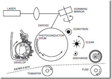
Electrophotographic printing involves a sequence of interacting processes which must be optimized collectively if quality printing is to be achieved. With respect to Fig. 23.12 they are as follows.

1. Charging of the photoconductor to achieve a uniform electrostatic surface charge can be done by means of a corona in the form of a thin, partially shielded wire maintained at several kilovolts with respect to ground (corotron). For positive voltages, a positive surface charge results from ionization in the vicinity of the wire. For negative voltages, negative surface charge is produced but by a more complex process involving secondary emission, ion impact, etc., that makes for a less uniform discharge. The precise design of the grounded shield for the corona can have a significant effect on the charge uniformity produced. To limit ozone production, many office printers (<20 ppm) employ a charge roller in contact with the

image

FIGURE 23.12 Schematic of the electrophotographic process. Dual component evelopment is shown with hot roll fusing and coronas for charging and cleaning. (Source: Durbeck, R.C. and Sherr, S. 1988. Hardcopy Output Devices. Academic Press, San Diego, CA. With permission.)

photoconductor. A localized, smaller discharge occurs in the gap between the roller and photoconductor, reducing ozone production between two and three orders of magnitude.

2. The charged photoconductor is exposed as described previously to form an image that will be at a significant voltage difference with respect to the background. The particular properties of the photoconductor in this step relate to electron hole generation by means of the light and the transport of either electron or hole to the surface to form the image. This process is photographic in nature and has a transfer curve reminiscent of the H and D curves for silver halide. The discharge must be swift and as complete as possible to produce a significant difference in voltage between charged and uncharged areas if optimum print quality is to be achieved. Dark decay must be held to a minimum and the PC must be able to sustain repeated voltage cycling without fatigue. In addition to having adequate sensitivity to the dominant wavelength to the exposing light, the PC must also have a wear-resistant surface, be insensitive to fluctuations in temperature and humidity, and release the toner completely to the paper at transfer. It is possible for either the discharged or the charged region to serve as the image to be printed. Widespread practice today, particularly in laser printers, makes use of the discharged area.

Early PCs were sensitive to visible wavelengths and relied on sulfur, selenium, and tellurium alloys. With the use of diode laser scanners, the need for sensitivity in the near infrared has given rise to organic photoconductors (OPC), which in their implementation consist of multiple layers, including a submicron- thick charge generation layer and a charge transport layer in the range of 30 µm thick. This enables the optimization of both processes and is in wide-spread use today. A passivation or wear layer is used for OPCs, which are too soft to resist abrasion at the transfer stage. In many desktop devices the photoconductive drum is embodied in a replaceable cartridge containing enough toner for the life of the photoconductor. This provides a level of user servicing similar to that for thermal ink jet printers having replaceable printheads.

3. Image formation is achieved by bringing the exposed photoconductor surface in contact with toner particles, which are themselves charged. Electrostatic attraction attaches these particles to form the image. Once again, uniformity is vital, as well as a ready supply of toner particles to keep pace with the development process. Two methods are in widespread use today: dual component, popular for high-speed printing and monocomponent toners commonly found in desktop printers. Dual component methods employ magnetic toner particles in the 10-µm range and magnetizable carrier beads whose characteristic dimension is around 100 µm. Mechanical agitation of the mixture triboelectrically charges the toner particles, and the combination is made to form threadlike chains by means of imbedded magnets in the development roller. This dense array of threads extending from the development roller is called a magnet brush and is rotated in contact with the charged photoconductor (Fig. 23.10). The toner is then attracted to regions of opposite charge and a sensor-controlled replenishment system is used to maintain the appropriate ratio of toner to carrier beads.

Monocomponent development simplifies this process by not requiring carrier beads, replenishment system, and attendant sensors. A much more compact development system results, and there are two implementations: magnetic and nonmagnetic. Magnetic methods still form a magnetic brush but it consists of toner particles only. A technique of widespread application is to apply an oscillating voltage to a metal sleeve on the development roller. The toner brush is not held in contact with the photoconductor but, rather, a cloud of toner particles is induced by the oscillating voltage as particles detach and reattach depending on the direction of the electric field. Nonmagnetic monocomponent development is equally popular in currently available printers. There are challenges in supplying these toners in charged condition and at rates sufficient to provide uniform development at the required print speed. Their desirability derives from lower cost and inherent greater transparency (for color printing applications) due to the absence of magnetic additives.

One way of circumventing the limitations on particle size and the need for some form of brush technique is to use liquid development. The toner is dispersed in a hydrocarbon-based carrier and is charged by means of the electrical double layer that is produced when the toner is taken into solution. Typically, the liquid toner is brought into contact with the photoconductor via a roller. Upon contact, particle transport mechanisms, such as electrophoresis, supply toner to the image regions. Fluid carryout is a major challenge

for these printers. To date this has meant commercial use where complex fluid containment systems can be employed. The technique is capable of competing with offset lithography and has also been used for color proofing.

4. The transfer and fuse stage imposes yet more demands on the toner and photoconductor. The toner must be released to the paper cleanly and then fixed to make a durable image (fusing). The majority of fusing techniques employ heat and pressure, although some commercial systems make use of radiant fusing by means of zenon flash tubes. The toner particles must be melted sufficiently to blend together and form a thin film, which will adhere firmly to the substrate. The viscosity of the melted toner, its surface tension, and particle size influence this process. The design challenge for this process step is to avoid excessive use of heat and to limit the pressure so as to avoid smoothing, that is, calendering and/or curling of the paper. Hot-roll fusing passes the toned paper through a nip formed by a heated elastomer-coated roller in contact with an unheated opposing roller that may or may not have an elastomer composition. Some designs also apply a thin film of silicone oil to the heated roller to aid in release of the melted toner from its surface. There is inevitably some fluid carryout under these conditions, as well as a tendency for the silicone oil to permeate the elastomer and degrade its physical properties. Once again materials innovation plays a major role in electrophotography.

5. The final phase involves removal of any remaining toner from the photoconductor prior to charging and imaging for the next impression. Common techniques involve fiber brushes, magnetic brushes, and scraper blades. Coronas to neutralize any residual charge on the PC or background toner are also typical components of the cleaning process. The toner removed in this step is placed in a waste toner hopper to be discarded. The surface hardness of the PC plays a key role in the efficiency of this step. Successful cleaning is especially important for color laser printers since color contrast can make background scatter particularly visible, for example, magenta toner background in a uniform yellow area.

Dot Microstructure

With respect to image microstructure, the design of the toner material, the development technique, and the properties of the photoconductor play key roles. It is desirable to have toner particles as small as possible and in a tightly grouped distribution about their nominal diameter. Composition of toner is the subject of a vast array of publications and patents. Fundamental goals for toner are a high and consistent charge-to-mass ratio, transparency in the case of color, a tightly grouped distribution, and a minimum, preferably no, wrong-sign particles. The latter are primarily responsible for the undesirable background scatter that degrades the print. Recent developments in toner manufacture seek to control this by means of charge control additives which aid in obtaining the appropriate magnitude of charging and its sign. Grayscale in laser printers is achieved by modulating the pulse width of the diode laser. The shape and steepness of the transfer curve, which relates exposure to developed density, is a function of photoconductor properties, development process, and toner properties. It is possible to produce transfer curves of low or high gradient. For text, a steep gradient curve is desirable, but for images a flatter gradient curve provides more control. Since the stability of the development process is subject to ambient temperature and humidity, the production of a stable grayscale color laser printer without print artifacts is most challenging.


Thermal Printing Technologies : Direct Thermal , Direct Thermal Transfer , Dye Diffusion Thermal Transfer and Resistive Ribbon Thermal Transfer

Thermal Printing Technologies

Printing technologies that employ the controlled application of thermal energy via a contacting printhead to activate either physical or chemical image formation processes come under this general classification. There are four thermal technologies in current use: direct thermal, direct thermal transfer, dye diffusion thermal transfer, and resistive ribbon thermal transfer.

Direct Thermal

This is the oldest and most prolifically applied thermal technology. The imaging process relies on the application of heat to a thermochromic layer of approximately 10 µm in thickness coated onto a paper substrate. The thermally active layer contains a leuco dye dispersed along with an acid substance in a binder. Upon heating fusion melting occurs resulting in a chemical reaction and conversion of the leuco dye into a visible deeply colored mark. Key to this process is the design of the printhead, which can be either a page-wide array or a vertical array or a scanning printhead. Two technologies are in use, thick film and thin film. Thick-film printheads have resistor material between 10 and 70 µm. The resistive material is covered with a glass layer approximately 10 µm thick for wear resistance. The thin-film printheads bear a strong resemblance to those found in thermal ink jet printheads. They employ resistive material, such as tantalum nitride, at 1 µm thickness and a 7-µm-thick silicon dioxide wear layer. Thin-film heads are manufactured in resolutions up to 400 dpi. In each case the resistors are cycled via electrical heating pulses through temperature ranges from ambient (25◦C) up to 400◦C. Overall, the thin-film printheads excel in energy efficiency conversion, print quality, response time, and resolution. For these reasons the thin-film printheads are used when high resolution is required, whereas the thick-film printhead excels in commercial applications such as bar coding, airline tickets, fax, etc.

image

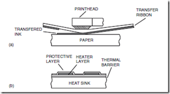
FIGURE 23.11 Schematic of wax transfer process: (a) Intimate contact between printhead, ribbon, and paper is required for successful transfer, (b) design elements of thin-film thermal printhead. Thermal barrier insulates heater for the duration of the heat pulse but allows relation of heater temperature between pulses.

Direct Thermal Transfer

These printers transfer melted wax directly to the paper (Fig. 23.11(a) and Fig. 23.11(b)). The wax that contains the colorant is typically coated at 4 µm thickness onto a polyester film, which, in common implementations, is approximately 6 µm thick. A thermal printhead of the kind described previously presses this ribbon, wax side down, onto the paper. As the individual heating elements are pulsed, the wax melts and transfers by adhesion to the paper. The process is binary in nature; but, by the use of shaped resistors, which produce current crowding via an hourglass shape, for example, the area of wax transferred can be modulated. Common implementations employ page width arrays at 300 dpi with some providing vertical addressability of 600 dpi. The thermal ribbons are also packaged in cassettes for scanning printhead designs in desktop and portable printers. Power consumption is an issue for all thermal printers, and efforts to reduce this for direct thermal transfer have focused on reducing the thickness of the ribbon.

Dye Diffusion Thermal Transfer

This technology involves the transfer of dye from a coated donor ribbon to a receiver sheet via sublimation and diffusion, separately or in combination. The amount of dye transferred is proportional to the amount of heat energy supplied; therefore, this is a continuous tone technology. It has found application as an alternative to silver halide photography, graphics, and prepress proofing. As with all thermal printers the energy is transferred via a transient heating process. This is governed by a diffusion equation and depending on the length of the heating pulse will produce either large temperature gradients over very short distances or lesser gradients extending well outside the perimeter of the resistor. Much of the design, therefore, focuses on the thicknesses of the various layers through which the heat is to be conducted. In the case of thermal dye sublimation transfer a soft-edged dot results, which is suitable for images but not for text. Shorter heating pulses will lead to sharper dots.

Resistive Ribbon Thermal Transfer

This technology is similar to direct thermal transfer in that a thermoplastic ink is imaged via thermal energy onto the substrate. The ribbon is composed of three layers: An electrically conductive substrate of polycarbonate and carbon black (16 µm thick), an aluminum layer 1000–2000 A˚ , and an ink layer which is typically 5 µm. The aluminum layer serves as a ground return plane. Heat is generated by passing current from an electrode in the printhead in contact with the ribbon substrate through the polycarbonate/carbon layer to the aluminum layer. The high pressure applied through the printhead ensures intimate contact with the paper, which does not have to be especially smooth for successful transfer. Printed characters can be removed by turning on all electrodes at a reduced energy level and heating the ink to the point that it

bonds to the character to be corrected but not to the paper. The unwanted character is removed as the printhead passes over it. This technology does not adapt to color printing in a straightforward way.


Nonimpact Printing Technologies :Ink Jet , Continuous Ink Jet , Drop On Demand (DOD) Ink Jet , Thermal Ink Jet/Bubble Jet DOD Printers , Piezoelectric DOD Printers , Grayscale Methods for DOD Ink Jet Printers , Ink and Paper for Ink Jet Devices

Nonimpact Printing Technologies
Ink Jet

The transfer process of ink jet printing is one of removing a drop of liquid ink from the bulk and giving it a velocity of sufficient precision and magnitude to place it on a substrate in close proximity to but not touching the printhead. There are three broad techniques: continuous, electrostatic, and drop on demand. Continuous ink jet printing, because of its intrinsic high drop rate, has tended to find more applications in commercial systems; electrostatic methods have yet to find widespread application, but have been used for facsimile recording; drop on demand, because of its simplicity and ease of implementation of color, has been widely accepted in the office and home market.

Continuous Ink Jet

The basic principle of continuous ink jet is to take advantage of the natural breakup process due to an instability in the jet that is formed when fluid is forced under pressure through a small orifice. This results from the interplay of surface tension and viscosity and takes place in a quasirandom manner unless external stimulation is applied. This breakup process was first studied by Rayleigh who characterized it via a growth rate for the instability, which depended on the jet diameter D, its velocity V , and the frequency F of any external stimulation. Rayleigh showed that the frequency for maximum growth rate of the instability was

   image

F = V/4.5D. By stimulating the jet at this frequency it is possible to obtain a uniform stream of droplets. The typical method of providing this stimulation today is via a piezoelectric transducer as an integral part of the printhead.

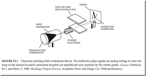
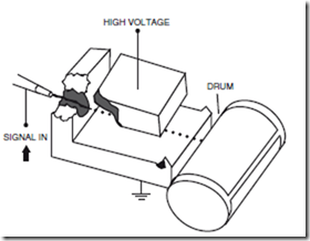
To make use of these droplets for printing it is necessary to charge them at breakoff. This is accomplished by placing electrodes in proximity to the breakup region of the jet. Deflection voltages are then applied farther downstream to direct the droplet to the substrate or into a collector for re- circulation and reuse. The earliest techniques in- volved charging the droplet and applying a variable deflection field to direct it to a specific spot on the paper, enabling full height characters to be printed in one pass (see Fig. 23.1). Later methods focused on producing a stream of charged droplets and using the printing (high-voltage) electrode to deflect unwanted drops for recirculation and reuse (Fig. 23.2). This technique, known as binary charged continuous ink jet, lends itself to the construction of multiple nozzle arrays, and there are a number of page-wide implementations in use.

Binary charged continuous ink jet with its high droplet rate makes a simple gray scaling technique possible. The dot on the paper is modulated in size by printing from one up to N droplets at the same location, where N is the number of different dot sizes desired. By operating at high frequencies and small drop volumes it is possible to produce sufficient gray levels such that full grayscale printing is achieved at reasonable print speeds. The most recent implementation of this method offers 512 gray levels at addressabilities between 200–300 pixels/in. To achieve the small fundamental droplet size, typical implementations employ glass capillaries with diameters of the order of 10 µm and are pressurized from 500–700 lb/in2. A color printhead will contain four capillaries, one for each color ink plus black.

image

FIGURE 23.2 Binary charged continuous ink jet. Droplets, charged at breakoff, are directed to the paper on a rotating drum. Droplets not selected for printing are diverted by the high-voltage electrode to be collected by a return gutter. (Source: Durbeck, R.C. and Sherr, S. 1988. Hardcopy Output Devices. Academic Press, San Diego, CA. With permission.

Drop On Demand (DOD) Ink Jet

For office and home applications the complexities of continuous ink jet technology, such as startup and shutdown procedures, ink recirculation, and the limited nozzle count, have led to the development of drop on demand ink jet technology. These devices employ unpressurized ink delivery systems and, as implied by their name, supply a drop only when requested. The basic technique employed is to produce a volume change in either the ink supply channel or an ink chamber adjacent to the nozzle such that the resulting pressure wave causes drop ejection. Refill is achieved by capillary forces and most DOD systems operate with a slight negative pressure at the ink reservoir. The mechanism for generating the pressure wave dominates the design of these devices, and there are two techniques extant in common DOD printers. One employs the pressure pulse derived from the vaporization of superheated fluid, and the other makes use of piezoelectric materials, which can be deformed by the application of electric potentials.

Devices employing the vaporization of superheated fluid are known concurrently as thermal ink jet or bubble jet printers, the choice of name depending on the manufacturer. Since drop on demand ink jets rely on capillary refill, their operational frequencies are much lower than for continuous ink jet devices. This stresses the importance of the compactness of the actuating system so as to achieve reasonable printing speeds via multiple nozzle printheads. The nozzles must also be precisely registered with respect to each other if systematic print artifacts are to be avoided.

image

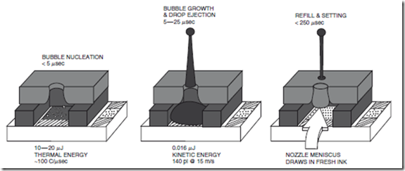
FIGURE 23.3 Drop ejection sequence for thermal ink jet. Nominal time frames and values for various parameters are given to indicate the scale of the three processes of nucleation, bubble growth, and jet formation followed by drop ejection and refill.

Thermal Ink Jet/Bubble Jet DOD Printers

When fluids are heated at extreme rates (e.g., 500 × 106 W/m2), they enter a short-lived metastable state where temperatures can far exceed the boiling point at atmospheric pressure. The difference between the elevated temperature and the boiling point is known as the degree of superheat. This process does not continue indefinitely, and all fluids have what is known as a superheat limit. At this point nucleation and vaporization will occur in the bulk of the fluid. These devices employ an electrically driven planar heater (typically, 50–60 µm2) in contact with the fluid. Under these conditions vaporization commences at the surface of the heater due to the presence of nucleation sites such as microscopic roughness. With correctly chosen heating rates this can be made very reliable. These heating rates lead to electrical pulse widths of 3–5 µs. In this time frame only a submicron portion of the fluid will be superheated. The net result is a vaporization pulse well in excess of atmospheric pressure and of approximately 3/4-µs duration. By locating a nozzle directly over or alongside the resistor this pressure pulse will eject a droplet (Fig. 23.3).

Within limits of the drop volume desired, it is found that the linear dimensions of the nozzle diameter and planar resistor are comparable. The actuator is therefore optimally compact, and this enables high- nozzle count printheads. The fabrication of the resistors is accomplished by photolithographic techniques common to the IC industry and the resistor substrates are silicon with a thin layer of insulating silicon dioxide. Precise registration from nozzle to nozzle is guaranteed under these circumstances, and electrical drive circuits may be integrated into the head to provide multiplexing capability. This is a valuable attribute for scanning printheads, which employ a flexible printed circuit for interconnect. These features have produced printheads currently numbering 300 or more nozzles for a single color. An additional benefit of the compactness of this technology is that the ink supply can be fully integrated with the print- head. This provides the user with virtually maintenance free operation as the printhead is replaced when the ink supply is consumed. Since the majority of problems arise from paper dust particles finding their way into a nozzle and occasionally becoming lodged there, printhead replacement provides for user service at reasonable cost. Some implementations feature a semipermanent printhead, which is supplied by ink from replaceable cartridges. The design choice is then a tradeoff involving many factors: frequency of maintenance, cost of operation, how often the printer is to be used, type of material printed, etc. The important subject of ink and paper for these printers will be taken up at the end of the section on DOD technologies.
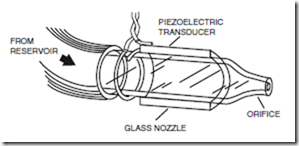
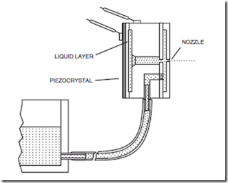
imageFIGURE 23.4 Squeeze tube piezoelectric ink jet. Early implementation of piezoelectric transducers for drop ejection. (Source: Advanced Technology Resources Corporation.)

Piezoelectric DOD Printers

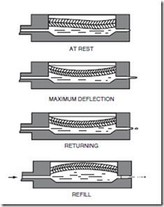
Crystalline structures, which develop a spontaneous dipole moment when mechanically strained, thereby distorting their crystal structures, are called piezoelectric. These materials may conversely be caused to be distorted via electrical potentials applied to the appropriate planes of the cyrstal. Piezoceramics have a polarization direction established during the manufacturing process, and the applied fields then interact with this internal polarization to produce mechanical displacement. Depending on the direction of the applied fields, the material can compress or extend longitudinally or transversely. These materials have found widespread use as transducers for DOD printers. An early form was that of a sleeve over a glass capillary, which terminated in a nozzle (Fig. 23.4). Depending on the location of the electrodes either a radial or longitudinal compression could be applied leading to a pressure wave in the enclosed ink sufficient to eject a droplet. Using the diameter of the nozzle as a unit of linear dimension, this approach placed the transducer well upstream from the nozzle (Fig. 23.5). Implementation of this design in a multinozzle printhead required careful matching of transducers and fluid impedance of the individual channels feeding each nozzle. This was a challenging task, and most designs bond a planar transducer to an ink chamber adjacent to a nozzle, as shown in Fig. 23.6.

image

FIGURE 23.5 Drop ejection sequence for piezoelectric printhead. Schematic of drop ejection via deflection of piezocrystal bonded to an ink capillary. In practice the piezodrivers were located well upstream of the nozzle due their size. (Source: Advanced Technology Resources Corporation.)

image

FIGURE 23.6 Design of Stemme Larson electric-driven DOD ink jet. Note the direct coupling of the pressure pulse to the ink chamber at the nozzle. (Source: Advanced Technology Resources Corporation.)

The method of directly coupling the piezoelectric transducer through an ink chamber to an exit nozzle has seen many enhancements and developments since its invention. A feature of some designs is that of air flow channeled at the orifice in such a way as to entrain the droplet as it exits the nozzle and to improve its directional stability, as well as to accelerate the droplet. This enables the device to be operated at lower transducer deflections and, therefore, at higher droplet rate since the settling time of the device has been reduced. Piezodevices can operate at elevated temperatures and are used to eject inks that are solid at room temperature. For solid inks the material is melted to a design temperature for appropriate viscosity and surface tension and then supplied to the piezoelectric-driven ink chamber. The ink then solidifies instantly on contact with the substrate.

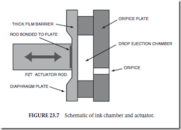
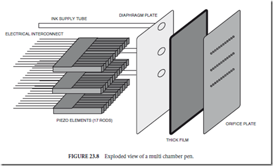
A more recent innovation employs piezoelectric transducers operated in the longitudinal mode. The transducers are formed from a single block of piezoceramic material in the form of an array of rods. Suitably placed potentials excite the rods to extend in the longitudinal direction. By bonding one end of the rod in contact with a thin membrane forming the base of an ink chamber, a pressure pulse is generated similar to that of the previous design (Fig. 23.7). To achieve sufficient pressure amplitude a diaphragm is used that is substantially larger than the orifice exit diameter. The consequence of this is that high nozzle

image

image

density printheads will require multiple rows of nozzles (Fig. 23.8). This design has been implemented to date with liquid inks only.

Grayscale Methods for DOD Ink Jet Printers

The drop rates for DOD devices are typically an order of magnitude less than those of continuous, pressurized systems. This dictates different strategies for the achievement of grayscale. Techniques are based on the generation of a few gray levels that, when incorporated into digital halftoning algorithms, such as error diffusion, clustered, dispersed dot, or blue-noise dither, produce a satisfactory grayscale. The number of levels necessary, their position relative to the maximum modulation achievable (i.e., maximum dot size or maximum intensity), and the specialized techniques employed in digital halftoning are an area of active research. There are many patents in the literature governing these techniques, and manufacturers seek to distinguish their devices by the technique offered. When combined with resolution enhancement methods mentioned in the section on print quality, printers with medium resolution, such as 300 dpi and 2 bits of grayscale, can produce remarkable results for both images, text, and graphics.

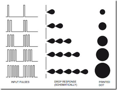
There are several methods available for DOD devices to modulate either the size or intensity of the dot. For piezodevices, pulse width modulation has been shown to produce droplets of different volumes and, therefore, dot sizes. All DOD ink jet devices have the option of ejecting a droplet repeatedly at the same location by passing over the same swath as many times as desired but this will affect throughput rates. Printheads with sufficient nozzle count can do this and still keep throughput rates within reason. For vapor bubble driven devices, a unique option exits by virtue of the short duration of the actuating bubble. Typical lifetime of bubbles in these devices, from vaporization through to bubble collapse, is of the order of 20 µs. If the resistor is pulsed shortly after bubble collapse, a second droplet can be ejected virtually on the tail of the initial droplet. This technique has been called multidrop in the literature. The ink chamber is fired under partial refill conditions, but with proper design several droplets can be ejected by this method at drop rates at around 40 kHz and having substantially the same volume (Fig. 23.9). These merge on the substrate to produce different dot sizes according to the number of droplets ejected for the location. This is not an option for most piezodevices due to the slower settling time of the actuator. Dye dilution methods have also been demonstrated as a way of modulating the intensity of the dot. If no halftone algorithm is employed, this will require many sets of nozzles to accommodate the different dye dilutions.

image

FIGURE 23.9 Stylized representation of multidrop process. Each input pulse consists of a group of drive pulses chosen for the final dot size desired. (Source: Durbeck, R.C. and Sherr, S. 1988. Hardcopy Output Devices. Academic Press, San Diego, CA. With permission.)

Ink and Paper for Ink Jet Devices
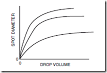
When liquid inks are employed the paper properties have a major impact on the print quality. The ink droplets will be absorbed by a substrate whose internal structure and surface energy will determine the size, shape, and overall microstructure of the drop. Paper, being a interlocking mesh of cellulose fibers with sizing and binding chemistry, is quite variable in nature. Figure 23.10 is a schematic indication of the response of paper to different volumes of ink. Note that it can be very nonlinear at low drop volumes and either flat or high gain at large volumes. The implication is that by simply changing the paper the print quality is altered. To control this variablity some papers are given a thin coat of claylike material containing whiteners, which are often fluorescent.

This coating presents a microporous structure that is more uniform than the cellulose fibers.

Dot formation on coated papers is therefore circular and more stable than on uncoated stock. Un-coated papers allow the ink to wick down the fibers producing an effect known as feathering of the dot.  In this case, microscopic tendrils of dye appear at the edge of the dot giving it and the overall print quality a blurred effect. This is particularly serious in the case of text printing, which benefits most fromsharp dot edges. Feathering is common for papers used in xerographic copiers. Bond paper, which is a popular office stock, is a partially coated paper and exhibits little feathering.

image

FIGURE 23.10 Paper response curves. The lower curve is typical of coated stock, which minimizes dot spread. (Source: Durbeck, R.C. and Sherr, S. 1988. Hardcopy Out- put Devices. Academic Press, San Diego, CA. With per- mission.)

Depending on the manufacturer, several techniques are employed to minimize the impact of paper variability on print quality. One method, the use of a heater, takes advantage of the fact that absorption into the paper does not commence immediately upon contact. There is a period known as the wetting time, which can be as long as 80 µs during which no absorption takes place. The application of heat immediately in the vicinity of the printhead swath can effectively “freeze the dot” by vaporizing carrier. This makes the printer insensitive to change in paper stock and provides uniformly high print quality regardless of substrate. Other methods make use of altering the fluid chemistry by means of surfactants, which increase penetration rate, and high vapor pressure additives to increase removal of fluid into the atmosphere. If the ink penetrates quickly then it is less likely to spread sideways and, thereby, dot size variation is lessened. When choosing a drop on demand ink jet printer, it is advisable to test the performance over the range of paper stocks to be used. In some cases it will be found that high-quality printing can only be obtained when a paper specified by the manufacturer is chosen.

With reference to the section on print quality, it should be kept in mind that the choice of paper will affect the overall dynamic range of print. Text printing, to be pleasing, needs to have an optical density of at least 1.3–1.4. For images, the more dynamic range the better, and special coated stock will always excel over copy paper if image quality is important. Many of the coated papers available still have a matte surface that diffusely reflects the light and limits the dynamic range for reasons previously discussed. Some manufacturers now offer a high-gloss substrate specifically intended for images. These substrates have a plastic base with special coatings to absorb the ink through to the substrate leaving a high gloss finish. This greatly improves the dynamic range to the point of approximating that of photographic paper. These substrates provide ink jet printers with the capability to produce highly saturated brilliant colors with exceptional chromatic and dynamic range and should be used if image printing is the primary objective. Besides excellent print quality there are other demands placed on the ink. It must provide reliable operation of the device and a durable image. By this it is meant that the image does not fade rapidly, that it is mechanically sound, that it cannot be easily removed from the paper, and that it is impervious to liquids. For liquid ink, this is a challenge since solvent-based color highlighter pens are commonly used to mark up printed documents. These solvents can cause the ink to smear depend- ing on the choice of ink chemistry and the manner in which the colorants are fixed to the substrate. These issues focus on colorant chemistry, and much research is applied to this problem. There are fade-proof dyes, but many are either incompatible with the ink vehicle, typically water, or are toxic or

mutagenic.


Printing Technologies

Printing Technologies

bigstock-The-use-of-fax-machines-49303736-1

The four basic elements of any printing technology are: addressing, marking substance and its storage and delivery, transfer of the marking substance, and fixing. Addressing refers to the communication of electronic data to the marking unit, typically via electronic or optical means. The marking substance contains the

colorant, vehicle/carrier material for transport, binders to secure the colorants to the paper, stabilizing agents to resist fading, and technology specific additives such as biocides for liquid inks. The transfer process is the fundamental physical mechanism whereby a specific amount of the marking substance is removed from the bulk and transferred to the paper. Fixing embodies the processes of adhesion, drying, or solidification of the material onto the paper to form a durable image. These fundamental subsystems interact with each other to give each printing technology its own unique characteristics. The common classification of printing technologies today begins with the broad separation into two classes: Impact and nonimpact printing technologies. Impact methods achieve transfer via the direct mechanical application of force or pressure via a marking element, which can be either a fine wire or fully formed character onto a colorant carrying ribbon in contact with the paper; the simplest form of this is a typewriter. Nonimpact methods cover a wide range of technologies that achieve transfer through a variety of means that may be either contact or noncontact in nature.


Introduction to Printing Technologies,Resolution and Addressability,Grayscale and Dot Microstructure

Introduction

Brother-DCP-J315W-Colour-Inkjet-Multifunction-Printer

The basic parameters of print quality are resolution, addressability, gray scale, and dot microstructure. A real device also has intrinsic variability in the printing process, producing visual artifacts, which come under the general heading of noise. Some of the more common manifestations of this are background scatter, dot placement errors, voids (due to nozzle malfunction in ink jet, for example), and banding in images. The significance of any of these aspects of print quality can only be determined by examining them with respect to the properties of the human visual system. The design choices of the basic print quality parameters are, therefore, guided by the properties of the human visual system to determine where improvement needs to be made or where little is to be gained by increasing any one of the specifications.

Resolution and Addressability

Resolution, the most widely used specification to rate print quality, is sometimes confused with the related term addressability. Fundamentally, resolution refers to the ability of the device to render fine detail. This simple definition is complicated by the fact that detail can be regarded as the fineness of the width of a line, the transition between white paper and printed intensity, and/or the smoothness of the edge of a curved line or a line printed at any arbitrary angle. In the simplest case, the resolution of a printer is defined as

the spacing of the dots such that full coverage is obtained, that is, no white paper can be seen. For circular dots placed on a square grid, this number would be calculated by dividing the diameter by the square root of two and taking its inverse. For example, an ideal 300 dots per inch (dpi) printer would produce 120-µm-diam dots at an 85 µm spacing. In practice, the dot would be made somewhat larger to allow for dot placement errors. This definition is best understood in terms of the finest line that can be printed by the device. At 300 dpi the line would exhibit a perceptible edge waviness, especially when printed at certain sensitive angles. This would also be true of curved lines. In addition, the range of lines of increasing thickness would have discontinuities since they would consist of an integral number of the basic line, each spaced at 85 µm. These issues have an important bearing on text print quality, which depends on the ability to render both curved and straight lines at variable widths.

The preceding definition is related to the specification of resolution with respect to the human visual system. In this case resolution is determined by the closeness of spacing between alternate black and white lines of equal width and defined contrast. These are known as line pairs and for a 300-dpi printer it would result in a value of 150 line pairs per inch. This is not strictly correct since the black lines would be wider than the white spaces due to the roundness of the dot. Since the human visual system has a response that approaches zero near 300 line pairs per inch, gains made in text print quality by increasing resolution alone can be expected to diminish above this value. At this point, issues such as print noise and grayscale enter if further improvement in print quality is desired.
To focus only on the resolution as defined in the previous paragraphs ignores the specific needs of the components of the printed material, that is, text and lines vs. images and area fill. Gains in text print quality may be had if the device can space the dots closer than the fundamental resolution. This can result in substantial dot overlap but allows the line width to be varied more continuously. In addition, at the edge of a curved line, the subpixel adjustments of individual dots increase the perception of smoothness commonly known as getting rid of the jaggies. This ultimate dot spacing of the device is called addressability. For example, printers employing this technique are specified as 300 × 600 dpi indicating a native resolution of 300 dpi in the horizontal direction and a vertical addressability of 600 dpi.

Grayscale

The ability of a printing technology to modulate the printed intensity on the page is referred to as its grayscale capability. There are three ways in which this may be accomplished: variation of the dot size, variation of the intensity of the printed dot, and digital halftoning techniques. The first two depend on the intrinsic properties of the technology, whereas digital halftoning can be employed by any printer. A printer that can continuously vary its intensity from white paper through to maximum colorant density is described as having continuous tone capability. Other technologies produce a modest number of intensity levels and make use of digital halftoning techniques to create a continuous tone effect. The manner in which gray scale is achieved is of obvious importance in image printing, particularly in the case of color. In recent years considerable effort has gone into the development of sophisticated digital halftoning algorithms to enable binary (single dot size and no intensity modulation) printers to render images. The resulting image quality depends more strongly on resolution than addressability. But the impact of even a few intrinsic gray levels on the print quality achieved by these algorithms can be dramatic.

An important parameter in grayscale considerations is that of the dynamic range, which is simply called range in the graphic arts. This is measured in terms of optical density, the negative logarithm of the reflectance. An optical density of 1.0 represents 10% of reflected light per instant flux, an optical density of 2.0 corresponds to 1% reflectance, and so on. For printed material the smoothness of the printed surface limits the maximum optical density obtainable. If the surface is smooth and mirrorlike, then the print appears glossy and can have optical densities approaching 2.4. The smooth surface reflects light in a specular manner and, therefore, scatters little stray light from the surface into the eye, and the color intensity is not desaturated. It is most noticeable in the case of photographic paper that has a high gloss finish. If the optical density range of the print is high, it is said to have high dynamic range and a very

pleasing image will result. Not all papers, however, are designed to have a glossy finish. Papers used in the office are also used in copiers and have a surface which produces diffuse reflection at the interface between the air and the paper. For most uncoated, nonglossy papers this will be between 3–4% and limits the maximum optical density to around 1.4. Image quality on these stocks will depend on the fixing of the colorant to the substrate to produce a smooth surface. The potential image quality for a printer is therefore a complex tradeoff involving the design choices of resolution, addressability, grayscale method, digital halftoning algorithm, paper stock, colorant, and fixing technology. Conclusion: for images, resolution alone is not a predictor of print quality.

Dot Microstructure

The microscopic nature of the dot produced by a given technology also has a bearing on final print quality. The most important parameter here relates to the edge gradient of the dot. Known as the normal-edge profile, it characterizes the transition between white paper and maximum colorant intensity, that is, the gradient of optical density that occurs at the edge of the dot and measures the steepness of the transition from white paper to full optical density. Some technologies, such as electrophotography, can vary this profile by adjusting various parameters in the imaging and developing process. For ink jet, various paper types will produce different normal-edge profiles. If the profile is very steep, that is, the transition occurs in a very small distance such as 5 µm, then the dot is described as being a hard dot or having a very sharp edge. This is desirable when printing lines and text that benefit from very sharp transitions between black and white. If this transition is gradual, the dot is described as being soft and produces a blurring of the edge, which can degrade the text quality. In the case of images, where smooth tones and tonal changes are desired, a soft dot can be very beneficial.

Hybrid Methods

From what has been said it should not be inferred that the needs of texts and images are in opposition. In recent years the intrinsic grayscale capability has been used to advantage in improving text print quality. The removal of jaggies can be greatly assisted by the combination of increased addressability and a few gray levels. By the use of gray levels in the region of the jagged stairstep, the transition can be made to take place over several pixels. This is, in essence, blurring the transition to make it less visible to the eye. In the case of certain fonts, there is fine detail requiring resolutions greater than the native resolution of the printer. This fine detail can be rendered through a combination of gray levels and regular pixels. The implementation of these methods requires a complex set of rules to be applied to the data bit stream before it is sent to the marking level of the printer. These rules draw heavily on image processing techniques and a knowledge of the human visual system and are proprietary. Skillfully applied they can have a dramatic effect on the text and line quality. There are a variety of trademarked names for these technologies designed to convey the sense of enhancement of the print quality.

The application of image processing techniques to manipulate the intrinsic properties of electronic printing technologies have made resolution an insufficient measure of print quality. A more comprehensive measure is needed to simplify the identification of the printing technology to serve the design goals for final output quality. Until such a metric is devised, the tradeoff analysis just described, implemented by means of industry standard test charts that separately probe the printer properties, will provide a predictive measure of print quality. Such test charts must also contain test images, which will be subject to the proprietary subjective image enhancement algorithms offered by the manufacturer.


Test On Digital Electronics Applications

Test On Digital Electronics Applications

Do not refer to the text when taking this test. You may draw diagrams or use a calculator if necessary. A good score is at least 38 correct answers. Answers are in the back of the book. It’s best to have a friend check your score the first time so you won’t memorize the answers if you want to take the test again.

1. A signal with a 100 ns time ‘‘On’’ and a 230 ns time ‘‘Off’’ has a frequency of:

(a) 30.3%

(b) 3 GHz

(c) 3 MHz

(d) 3 kHz

2. A toggle flip flop will divide a clock frequency by:

(a) The value selected in its inputs

(b) 2

(c) 1.5, but the output duty cycle is 50%

(d) The toggle flip flop is used for debouncing switch inputs

3. The NPN transistor relaxation oscillator is well suited for:

(a) High-speed computer applications

(b) Only audio applications

(c) Low-cost applications where accuracy isn’t important

(d) Power supply duty cycle generators

4. If you wanted an oscillator that produced a period of 4 gate delays, you would:

(a) Use a standard ring oscillator

(b) Use something other than a ring oscillator

(c) Use two three inverter ring oscillators and XOR their outputs

(d) Use a two inverter ring oscillator and divide the output frequency by two using a toggle D flip flop

5. The duty cycle of a ring oscillator is:

(a) Always 50%

(b) Equal to the number of inverters used in the ring oscillator multiplied by the gate delay

(c) Dependent on the technology used in the inverters

(d) Always 100%

6. Why are TTL inverters not recommended for relaxation oscillators?

(a) They are too costly

(b) They do not operate at a fast enough speed

(c) Their current controlled inputs will affect the operation of the oscillator

(d) They may short out internally when used as part of an oscillator.

7. A relaxation oscillator has an R1 value of 1k, C of 0.1 mF and R2 equal to 10 k. What frequency will it oscillate at?

(a) It won’t oscillate

(b) 4.54 kHz

(c) 4.54 MHz

(d) 4.54 Hz

8. Crystals used in oscillators are:

(a) Relatively high cost but very accurate

(b) Very robust and immune to shock damage

(c) Low cost with an accuracy that is similar to that of a ‘‘canned oscillator’’

(d) Mined in South America

9. The crystal inverter circuit requires the following parts:

(a) Crystal and inverter

(b) Crystal, inverter, two capacitors and two resistors

(c) Crystal, inductor, three resistors, two capacitors and an NPN transistor

(d) Crystal, diode, two capacitors, hand wound coil, two diodes

10. Changing the voltage at the ‘‘Vcontrol’’ pin of a 555 astable oscillator:

(a) Will change the period of the oscillator output

(b) Won’t change anything

(c) Will lower the amount of power consumed

(d) Will add unnecessary costs to the circuit

11. A 555 astable oscillator with R1 ¼ 47 k, R2 ¼ 100 k and C ¼ 4.7 mF will oscillate at:

(a) 805 Hz

(b) 0.805 Hz

(c) 1.24 Hz

(d) 1.24 kHz

12. Decreasing value of a resistor or capacitor in a 555 monostable will:

(a) Lower its operating frequency

(b) Raise its operating frequency

(c) Increase the pulse width

(d) Decrease the pulse width

13. A chip with two 555 timers built in has the part number: (a) 75555

(b) 556

(c) No such chip exists

(d) 2×555

14. The delay in a ‘‘canned delay line’’ is produced by:

(a) Elves

(b) A piece of quartz, cut to provide a specified delay

(c) A long piece of copper wire, formed as a coil

(d) A large array of simple gates

15. Why is reset passed to the ‘‘Output Formatter’’ in the sequential circuit block diagram?

(a) To control the operation of tri-state drivers built into the ‘‘Output Formatter’’

(b) To synchronize outputs with the operation of the chip

(c) To minimize power usage when the chip is reset

(d) To speed up operation of the sequential circuit

16. To create a cascaded counter from multiple chips, what signal(s) are passed between the chips?

(a) The most significant two bits

(b) The ‘‘Carry’’ from the least significant counter and the ‘‘Borrow’’ from the more significant counter

(c) Just the carry from the least significant counter to the clock input of the more significant counter

(d) The clock and chip enable signals to be shared between the two counters

17. What are the disadvantages of serial data transmission over parallel data transmission?

(a) Increased product chip count

(b) Slower data transmission

(c) Increased product power requirements

(d) Increased data error rate

18. The linear feedback shift register polynomial defines:

(a) The XOR ‘‘taps’’ used to modify the incoming data

(b) The execution order of magnitude

(c) The value needed to decode any value run through the LFSR

(d) The relationship between the number of bits and speed of the LFSR’s operation

19. The number of states and inputs in a hardware state machine are a function of:

(a) The fanout capabilities of the chips used

(b) The number of discrete states required

(c) The requirements of the application

(d) The size of the ROM used

20. Since commands to a Hitachi 44780 controlled LCD require 160 ms or more to execute, what is an effective way of waiting the suggested delay before sending the next command?

(a) Using a 555 timer wired as a monostable

(b) Passing requests to the LCD through an RC delay

(c) Polling the busy flag

(d) Using a clock with a 5 ms period

21. What signal is not included in a typical sequential logic circuit interface bus?

(a) _Read

(b) Data Read Ready

(c) _Write

(d) Address Bit 0

22. A ‘‘three to eight’’ decoder:

(a) Cannot be implemented in TTL or CMOS Logic

(b) Converts three data selects into eight device read requests

(c) Converts three clock cycles into eight state machine addresses

(d) Converts three binary bits into eight interface device selects

23. The segments to be turned on in a seven-segment LED display is determined by:

(a) A circuit which enables the common cathodes or common anodes in the LED displays

(b) A microprocessor built into each seven-segment LED display

(c) A combinatorial circuit performing Boolean arithmetic operations on the display bits

(d) A sequential circuit that compares the display bits to expected values

24. A PWM with a period of 10 ms and a ‘‘high’’ signal of 4 ms has a duty cycle of:

(a) Not enough information is available to determine the duty cycle

(b) 60%

(c) 0.4

(d) 40%

25. To produce a PWM output signal of 20 kHz and have 6 bits of accuracy, what input clock frequency should be used?

(a) 20 kHz

(b) 64 Hz

(c) 1.28 MHz

(d) 5.1 MHz

26. The two inverter debounce circuit is best suited for what kind of input devices?

(a) Push buttons

(b) 40%

(c) 0.4

(d) Double throw switches

27. Hysteresis causes logic inputs to be registered:

(a) Faster than normal inputs

(b) At lower thresholds than devices with standard inputs

(c) At more extreme thresholds than devices with standard inputs

(d) When there is an inductor on the line

28. A switch matrix keypad is:

(a) Used by Trinity and Neo to access the Matrix

(b) A two-dimensional array of switches used to provide multiple button inputs

(c) A series of switches that change the output signal of a

sequential circuit

(d) The natural evolution of a single button to multiple buttons

29. The Princeton architecture was criticized because:

(a) The single memory interface was felt to be a performance bottleneck

(b) It relied too heavily on vacuum tube technology

(c) The design was taken from other, earlier computer designers

(d) The amount of space required for it seemed to be prohibitive

30. The first digit to the right of the decimal point in a binary floating point number has a value of:

(a) 0.1 decimal

(b) 0.25 decimal

(c) 0.5 decimal

(d) 1.0 decimal

31. Floating point numbers are stored in data size except:

(a) 2 bytes

(b) 4 bytes

(c) 8 bytes

(d) 10 bytes

32. SRAM memory is best suited for applications which require:

(a) Data stacks

(b) Gigabytes of memory

(c) Mass storage of data

(d) Fast data access for a relatively large memory area

33. Stacks cannot be modeled by:

(a) Trays in a lunchroom

(b) Pieces of paper on a person’s desk

(c) Stacks of paper produced by a computer processor

(d) A jelly bean jar

34. The operation of the Zener regulator is analogous to:

(a) A car’s carburetor

(b) A bowl with a hole cut in the bottom

(c) A PWM output driven by a comparator

(d) A comparator output driven by sensor

35. The operation of the linear regulator is analogous to:

(a) A car’s carburetor

(b) A bowl with a hole cut in the bottom

(c) A PWM output driven by a comparator

(d) A comparator output driven by sensor

36. A 10:1 transformer has an input of 110 volts AC. What is its output?

(a) 11 volts DC

(b) 11 volts AC

(c) 110 volts DC

(d) 11 amps AC

37. ‘‘PAL’’ I/O pins are:

(a) Input and Output

(b) Programmable Input or Output

(c) Input only

(d) Output only

38. What is not a ‘‘local memory’’ device:

(a) Processor cache

(b) PCI status registers

(c) Main memory (S)DRAM

(d) Processor ROM

39. The Logic levels for the PC’s parallel port are?

(a) 3.3 volt CMOS Logic compatible

(b) 5 volt TTL/CMOS Logic compatible

(c) 5 volt ‘‘HCT’’ Logic compatible

(d) Current controlled, voltage levels are not considered

40. The inventor of the parallel port pinout standard was:

(a) IBM

(b) Apple Computers

(c) The Centronics Corporation

(d) Xerox FARC

41. The ‘‘Data’’ bits of the PC’s parallel port have what kind of outputs?

(a) Discrete transistors

(b) CMOS totem pole outputs

(c) Pulled up Open Collectors that can be changed by external

devices

(d) TTL tri-state buffers

42. ‘‘Vertical synch’’ in a video display:

(a) Moves the electron beam in the CRT to the left

(b) Moves the electron beam in the CRT to the top

(c) Starts the raster going up and down

(d) Is needed for CRTs pointing upwards

43. The ‘‘NTSC’’ video standard was first developed for:

(a) Military radar screens

(b) Portable news gathering services

(c) Electronic instruments

(d) Televisions

44. The ‘‘Microwire’’ synchronous serial protocol sends:

(a) A word consisting of 16 bits of data

(b) A word consisting of 8 bits of data

(c) Status Information before Data

(d) Command Information before Data

45. I2C’s ‘‘Acknowledge’’ bit:

(a) Is used as a ‘‘Parity Bit’’ for Received Data

(b) Indicates the Received Data was Valid

(c) Is a placeholder in case 9 bits of data is required

(d) Is not currently implemented, but will be in the future

46. Baudot asynchronous serial communications was developed for:

(a) Networking

(b) Televisions

(c) Teletypes

(d) Telegraphs

47. What are the differences between Baudot asynchronous serial communications and NRZ serial communications?

(a) None

(b) The number of bits transmitted

(c) The speed at which data is transmitted

(d) The number of ‘‘overhead’’ bits

48. The primary difference between Manchester Encoding and NRZ is:

(a) The media used to transmit the data

(b) The bit timing for ‘‘0’’ and ‘‘1’’ change in Manchester Encoding

(c) The data rates used to transmit the data

(d) The companies that hold the original patents on the technologies

49. To implement a three wire RS-232 connection, you will have to tie together:

(a) RTS/CTS and DSR/DTR

(b) RI/CTS and DSR/RTS

(c) DCD/DSR and RTS/CTS

(d) DCD/CTS and RI/DSR

50. The RS-232 to TTL/CMOS level translator shown in Fig. Test 2.1:

(a) Is an inexpensive, full capability RS-232 interface

(b) Sends data in ‘‘half duplex’’ mode only

(c) Can be used for handshaking lines as well as RX and TX

(d) Is limited by the speed it can operate at

image


PC Interfacing Basics :Synchronous Serial Interfaces (SPI, I2C, Microwire) ,Asynchronous Serial Interfaces and RS-232 Electrical Standards

Synchronous Serial Interfaces (SPI, I2C, Microwire)

There are two very common synchronous data protocols, Microwire and SPI, from which a variety of standard devices (memory and peripheral functions) have been designed around, including serial EEPROMs, sensors and other I/O functions. I consider these protocols to be methods of transferring synchronous serial data rather than intelligent network protocols because each device is individually addressed (even though the clock/data lines can be common between multiple devices). If the chip select for the device is not asserted, the device ignores the clock and data lines. With these protocols, only a single ‘‘Master’’ can be on the bus. Normally, just eight bits of data are sent out at a time. For protocols like Microwire where a ‘‘Start bit’’ is initially sent, the ‘‘Start bit’’ is sent using direct reads and writes to the I/O pins. To receive data, a similar circuit would be used, but data would be shifted into the shift register and then read by the microcontroller.

The Microwire protocol is capable of transferring data at up to one megabit per second. Sixteen bits are only transferred at a time. After selecting a chip and sending a start bit, the clock strobes out an eight bit command byte, followed by (optionally) a 16 bit address word transmitted and then another 16 bit word either written or read by the microcontroller.

With a one megabit per second maximum speed, the clock is both high and low for 500 ns. Transmitted bits should be sent 100 ns before the rising edge of the clock. When reading a bit, it should be checked 100 ns before the falling edge of the clock. While these timings will work for most devices, you should make sure you understand the requirements of the device being interfaced to.

 The SPI protocol is similar to Microwire, but with a few differences:

1. SPI is capable of up to 3 megabits per second data transfer rate.

2. The SPI data ‘‘word’’ size is eight bits.

3. SPI has a ‘‘Hold’’ which allows the transmitter to suspend data transfer.

4. Data in SPI can be transferred as multiple bytes known as ‘‘Blocks’’ or ‘‘Pages’’.

Like Microwire, SPI first sends a byte instruction to the receiving device. After the byte is sent, a 16 bit address is optionally sent followed by eight bits of I/O. As noted above, SPI does allow for multiple byte transfers. An SPI data transfer is shown in Fig. 13-12. The SPI clock is symmetrical (an equal low and high time). Output data should be available at least 30 ns before the clock line goes high and read 30 ns before the falling edge of the clock.

When wiring up a Microwire or SPI device, one trick that you can do to simplify the microcontroller connection is to combine the ‘‘DI’’ and ‘‘DO’’ lines into one pin, as was shown earlier in the book.

The most popular form of microcontroller network is ‘‘I2C’’, which stands for ‘‘Inter-Intercomputer Communications’’. This standard was originally developed by Philips in the late 1970s as a method to provide an interface between microprocessors and peripheral devices without wiring full address, data and control busses between devices. I2C also allows sharing of network resources between processors (which is known as ‘‘Multi-Mastering’’). Your PC probably has several I2C busses built into it for controlling system control and monitoring functions.

The I2C bus consists of two lines: a clock line (‘‘SCL’’) which is used to strobe data (from the ‘‘SDA’’ line) from or to the master that currently has control over the bus. Both these bus lines are pulled up (to allow multiple devices to drive them). A I2C controlled stereo system might be wired as shown in Fig. 13-13.

The two bus lines are used to indicate that a data transmission is about to begin as well as pass the data on the bus. To begin a data transfer, a ‘‘Master’’ puts a ‘‘Start Condition’’ on the bus. Normally, when the bus is in

image


image

the ‘‘Idle State’’, both the clock and data lines are not being driven (and are pulled high). To initiate a data transfer, the master requesting the bus pulls down the SDA bus line followed by the SCL bus line. During data transmission this is an invalid condition (because the data line is changing while the clock line is active/high). Each bit is then transmitted to or from the ‘‘Slave’’ (the device the message is being communicated with by the ‘‘Master’’) with the negative clock edge being used to latch in the data. To end data transmission, the reverse is executed; the clock line is allowed to go high, which is followed by the data line.

Data is transmitted in a synchronous (clocked) fashion. The most

significant bit is sent first and after eight bits are sent, the master allows the data line to float (it doesn’t drive it low) while strobing the clock to allow the receiving device to pull the data line low as an acknowledgment that the data was received. After the acknowledge bit, both the clock and data lines are pulled low in preparation for the next byte to be transmitted or a Stop/ Start Condition is put on the bus. Fig. 13-14 shows the data waveform.

Sometimes, the acknowledge bit will be allowed to float high, even though the data transfer has been completed successfully. This is done to indicate that the data transfer has completed and the receiver (which is usually a ‘‘slave device’’ or a ‘‘Master’’ which is unable to initiate data transfer) can prepare for the next data request.

There are two maximum speeds for I2C (because the clock is produced by a master, there really is no minimum speed). ‘‘Standard Mode’’ runs at up to 100 kbps and ‘‘Fast Mode’’ can transfer data at up to 400 kbps.

Asynchronous Serial Interfaces

Understanding how asynchronous serial communications works is easy; implementing them on a PC is frustrating and hard and used to be especially true for casual PC owners. This situation is improving with newer high-speed interface connection protocols (USB and Firewire), but actually sitting down and getting RS-232 communication between two devices working can be a pain. Much of the information I will present on RS-232 in this section will seem quite obvious, but I urge you to read through this material as there are some tricks and information contained here that could probably get you out of a bind or two.

Asynchronous long distance communications came about as a result of the Baudot ‘‘teletype’’. This device mechanically (and, later, electronically) sent a string of electrical signals (which we would call ‘‘bits’’), like the one shown in Fig. 13-15, to a receiving printer. This data packet format is still used today for the electrical asynchronous transmission protocols described in the following sections. With the invention of the teletype, data could be sent and retrieved automatically without having an operator having to sit by the teletype all night unless an urgent message was expected.

The Baud Rate specified for the data transmission is the maximum number of possible data bit transitions per second (measured in ‘‘bits per second’’, abbreviated to ‘‘bps’’). This includes the ‘‘Start’’, ‘‘Parity’’ and ‘‘Stop’’ bits at the ends of the data ‘‘packet’’ shown in Fig. 13-15 as well as the five data bits

image

in the middle. I use the term ‘‘packet’’ because we are including more than just data (there is also some additional information in there as well), so ‘‘character’’ or ‘‘byte’’ (if there were eight bits of data) are not appropriate terms. This means that for every five data bits transmitted, eight bits in total are transmitted (which means that nearly 40% of the data transmission bandwidth is lost in teletype asynchronous serial communications).

The ‘‘Data Rate’’ is the number of data bits that are transmitted per second. For this example, if you were transmitting at 110 baud, the actual data rate is 68.75 bits per second (or, assuming five bits per character, 13.75 characters per second).

With only five data bits, the Baudot code could only transmit up to 32

distinct characters. To handle a complete character set, a specific five-digit code was used to notify the receiving teletype that the next five-bit character would be an extended character. With the alphabet and most common punctuation characters in the ‘‘primary’’ 32, this second data packet wasn’t required very often. In the data packet shown in Fig. 13-15, there are three control bits. The ‘‘Start Bit’’ is used to synchronize the receiver to the incoming data. In most hardware circuits designed to read an asynchronous serial packet, there is an overspeed clock running at 16 times the incoming bit speed which samples the incoming data and verifies whether or not the data is valid. When waiting for a character, the receiver hardware polls the line repeatedly at 1/16 bit period intervals until a ‘‘0’’ (‘‘Space’’) is detected (down arrow at the left of Fig. 13-16). The receiver then waits half a cycle before

image

polling the line again to see if a ‘‘glitch’’ was detected and not a Start bit. This polling takes place in the middle of each bit to avoid problems with bit transitions (or if the transmitter’s clock is slightly different from the receivers, the chance of misreading a bit will be minimized).

Once the Start bit is validated, the receiver hardware polls the incoming data once every bit period multiple times (again to ensure that glitches are not read as incorrect data).

The ‘‘Stop’’ bit was originally provided to give both the receiver and the transmitter some time before the next packet is transferred (in early computers, the serial data stream was created and processed by the computers and not custom hardware, as in modern computers).

The ‘‘Parity’’ bit is a crude method of error detection that was first brought in with teletypes. The purpose of the parity bit is to indicate whether the data was received correctly. An ‘‘odd’’ parity meant that if all the data bits and parity bits set to a ‘‘Mark’’ were counted, then the result would be an odd number. ‘‘Even’’ parity is checking all the data and parity bits and seeing if the number of ‘‘Mark’’ bits is an odd number. Along with even and odd parity, there are ‘‘Mark’’, ‘‘Space’’ and ‘‘No’’ parity. ‘‘Mark’’ parity means that the parity bit is always set to a ‘‘1’’, ‘‘Space’’ parity is always having a ‘‘0’’ for the parity bit and ‘‘No’’ parity is eliminating the parity bit all together. I said that parity bits are a ‘‘crude’’ form of error detection because they can only detect one bit error (i.e. if two bits are in error, the parity check will not detect the problem). If you are working in a high induced noise environment, you may want to consider using a data protocol that can detect (and, ideally, correct) multiple bit errors.

The most common form of asynchronous serial data packet is ‘‘8-N-1’’, which means eight data bits, no parity and one stop bit. This reflects the capabilities of modern computers to handle the maximum amount of data with the minimum amount of overhead and with a very high degree of confidence that the data will be correct.

Having reviewed the data protocol for asynchronous serial communications, let’s go on and look at the electrical specifications, starting with the connectors that you will find on the back of your PC (Fig. 13-17). Either a male 25 pin or male 9 pin connector is available on the back of the PC for each serial port – chances are you will have a 9 pin connector because it takes up the least amount of space.

Working with MS-DOS in early systems, only a maximum of four serial ports could be addressed by the PC, and of these probably only two were useable for connecting external devices to the PC due to conflicts with other hardware devices. In modern systems, which have ‘‘Plug and Play’’ capabilities and the Windows operating system, which can allocate resources

image

throughout the system, the number of standard serial ports has been greatly expanded. My personal record is 64 serial devices for environmental chamber status test software.

The standard RS-232 data rates available to you in the PC are listed in Table 13-2. As an interesting exercise, I suggest that you find the reciprocal of the data rates listed in Table 13-2, multiply by 1,000,000 and then divide by 13 – what you will find is that the results for the data rates starting at 1200 bps and going higher will have a very small fraction. In fact, the error will be much less than 0.1%! This is a good trick to keep in your hip pocket when you have to implement an RS-232 interface and you don’t have any crystals that have been cut specifically to provide a multiple of these data rates.

Asynchronous communications based on the Baudot teletype/RS-232 is known as ‘‘Non-Return to Zero’’ (‘‘NRZ’’) asynchronous communications, because at the end of each data packet the serial line is high. There are other methods of sending asynchronous serial data, with one of the most popular being ‘‘Manchester encoding’’. In this type of data transfer, each bit is synchronized to a ‘‘start’’ bit and the following ‘‘Data Bits’’ are read with the ‘‘space’’ dependent on the value of the bit.

Manchester encoding is unique in that the ‘‘Start Bit’’ of a packet is quantitatively different from a ‘‘1’’ or a ‘‘0’’ (shown in Fig. 13-18). This allows a receiver to determine whether or not the data packet being received is actually at the start of the packet or somewhere in the middle (and should be ignored until a start bit is encountered).

image

image

Manchester encoding is well suited for situations where data can be easily interrupted or there is a conflict in the middle of data reception. Because of this, it is the primary method of data transmission for infrared control (such as used in your TV’s remote control).

RS-232 Electrical Standards

In the previous section, I didn’t tell the whole story about RS-232 asynchronous serial communications. I left out one very important point – signals do not travel at the same voltage levels as what we’ve discussed so far in the book. When RS-232 was first developed into a standard, computers and the electronics that drive them were still very primitive and unreliable. Because of that, we’ve got a couple of legacies to deal with and this can complicate connecting digital electronics circuits to another device using RS-232.

The biggest concern is the voltage levels of the data. A ‘‘Mark’’ (‘‘1’’)

is specified to be -3 volts to -12 volts and a ‘‘Space’’ (‘‘0’’) is þ3 volts to þ12 volts. This means that there must be some kind of voltage level conversion when passing RS-232 to or from digital electronic devices. There are a number of ways of doing this.

Before working with the voltage levels, I just want to say a few words about the ‘‘handshaking’’ signals built into RS-232 (these are all the RS-232 connections other than RX, TX and GND in Fig. 13-17). These six additional lines (which are at the same logic levels as the transmit/receive lines) are used to interface between devices and control the flow of information between computers.

The ‘‘Request To Send’’ (‘‘RTS’’) and ‘‘Clear To Send’’ (‘‘CTS’’) lines are used to control data flow between the computer (‘‘DCE’’) and the modem (‘‘DTE’’ device). The ‘‘Data Transmitter Ready’’ (‘‘DTR’’) and ‘‘Data Set Ready’’ (‘‘DSR’’) lines are used to establish communications. There are two more handshaking lines that are available in the RS-232 standard that you should be aware of, even though chances are you will never connect anything to them. The first is the ‘‘Data Carrier Detect’’ (‘‘DCD’’), which is asserted when the modem has connected with another device (i.e. the other device has ‘‘picked up the phone’’). The ‘‘Ring Indicator’’ (‘‘RI’’) is used to indicate to a PC whether or not the phone on the other end of the line is ringing or if it is busy. Few of these lines are used in modern RS-232 applications and, as shown in Fig. 13-19, the DTR/DSR and CTS/RTS pairs are often simply shorted together to avoid any ‘‘hardware handshaking’’ issues with the PC. There is a common ground connection between the DCE and DTE devices. This connection is critical for the RS-232 level converters to determine the actual incoming voltages. The ground pin should never be connected to a chassis or shield ground (to avoid large current flows or be shifted and prevent accurate reading of incoming voltage signals). Incorrect grounding of an application can result in the computer or the device it is

image

interfacing having to reset or have they power supplies blow a fuse or burn out. The latter consequences are unlikely, but I have seen it happen in a few cases. To avoid these problems make sure that chassis and signal grounds are separate or connected by a high value (hundreds of k Q) resistor.

The most popular method for converting TTL/CMOS Logic signals to RS-232 levels is to use the MAXIM MAX232 (see Fig. 13-20,) which has a built in charge-pump voltage generator. This chip is ideal for implementing three-wire RS-232 interfaces (or to add a simple DTR/DSR or RTS/CTS handshaking interface). Ground for the incoming signal is normally connected to the digital electronics ground. Along with the MAX232,

MAXIM and some other chip vendors have a number of other RS-232 charge-pump equipped devices that will allow you to handle more RS-232 lines (to include the handshaking lines). Some charge-pump devices that are also available do not require the external capacitors that the MAX232 chip does, which will simplify the layout of your circuit (although these chips do cost quite a bit more).

The next method of translating RS-232 and TTL/CMOS voltage levels is to use the transmitter’s negative voltage as the circuit, as Fig. 13-21 shows.

This circuit relies off of the RS-232 communications, only running in ‘‘Half- Duplex’’ mode (i.e. only one device can transmit at a given time). When the external device wants to transmit to the PC, it sends the data either as a ‘‘Mark’’ (leaving the voltage being returned to the PC as a negative value) or as a ‘‘Space’’ by turning on the transistor and enabling the positive voltage output to the PC’s receivers. If you go back to the RS-232 voltage specification drawing, you’ll see that þ5 volts is within the valid voltage range for RS-232 ‘‘Spaces’’. This method works very well (consuming just about no power) and is obviously a very cheap way to implement a three-wire RS-232 bi-directional interface. There is a chip, the Dallas Semiconductor DS275, which incorporates the circuit above (with a built-in inverter) into the single package shown, making the RS-232 very simple.

Before finishing, I want to make a final point on three wire RS-232 connections. The first is that it cannot be implemented blindly; in about 20% of the RS-232 applications that I have had to do over the years, I have had to implement some subset of the total seven wire (transmit, receive, ground and four handshaking lines) protocol lines. Interestingly enough, I have never had to implement the full hardware protocol. This still means that four out of five times if you wire the connection as shown in Fig. 13-19, the application would have worked.

image

Quiz

1. Which type of memory responds in the least amount of time?

(a) Processor cache

(b) All three types respond equally fast

(c) Main Memory (S)DRAM

(d) Processor ROM

2. What is not a characteristic of a computer bus?

(a) Controlled by a central processor

(b) The ability of peripherals on the bus to request information

(c) Data can be read/written to peripheral busses

(d) Keeping a log of the processor bus accesses

3. The minimum timing between signal edges in the parallel port is:

(a) 0.5 ms

(b) 0.5 ms

(c) 0.5 ns

(d) There are no delays; the port works completely asynchronously

4. The raster display on a video display looks like:

(a) A series of parallel lines going across the display

(b) Parallel lines that loop back like plough lines in a farmer’s field

(c) A series of small dots drawn on the video display

(d) A series of brush strokes on the video display

5. ‘‘Horizontal synch’’ in a video display:

(a) Moves the electron beam in the CRT to the left

(b) Moves the electron beam in the CRT to the top

(c) Starts the raster going side to side

(d) Is needed for CRTs laid down on their side

6. Devices on a synchronous serial bus are normally referred to as:

(a) ‘‘Dominant’’ and ‘‘Recessive’’

(b) ‘‘Master’’ or ‘‘Slave’’

(c) ‘‘1’’ or ‘‘0’’

(d) ‘‘Transmitter’’ or ‘‘Receiver’’

7. The maximum speed of the ‘‘SPI’’ synchronous serial protocol is:

(a) 100 kpbs (thousands of bits per second)

(b) 1 Mbps (millions of bits per second)

(c) 2 Mbps

(d) 3 Mbps

8. To connect to a modern PC’s RS-232 connector, you will need:

(a) Fiber optic cable

(b) 75 Ohm Coax and BNC connector

(c) RJ-45 cable and crimper

(d) A 9 pin male D-Shell connector

9. The RS-232 voltage levels of -12 volts for a ‘‘1’’ and þ12 volts for ‘‘0’’ means that:

(a) You can connect digital electronics devices directly to RS-232 connections

(b) You can connect TTL/CMOS Logic drivers directly to RS-232

(c) You can connect TTL/CMOS Logic inputs directly to RS-232

(d) You cannot connect digital electronics devices directly to RS- 232 connections

10. The MAX232:

(a) Uses a charge pump to power the circuit

(b) Requires þ12 volts and -12 volts to convert TTL/CMOS Logic signals

(c) Produces correct RS-232 voltages and converts TTL/CMOS Logic signals

(d) Will allow a full RS-232 connection with only one chip


PC Interfacing Basics : The Parallel (Printer) Port and Video Output

PC Interfacing Basics

From a practical point of view, chances are you will be designing an interface or enhancement to your PC. Most modern commercial devices utilize USB ports, but you can still do a lot of interesting projects with the ‘‘legacy’’ interfaces built into the PC. Along with this, a basic understanding of your PC will help you understand how commercial products are designed and may give you some ideas as to how you can design your own complex applications.

The PC ‘‘core’’ circuitry consists of the microprocessor, memory, the interrupt controller and a DMA controller, as shown in Fig. 13-1. This set of hardware can run any program or interface with hardware attached to this ‘‘local bus’’. While you may think of processor memory in terms of the megabytes that were advertised when you bought the PC, there are actually three different types of memory that are accessed.

The term ‘‘local memory’’ is kind of a loosely defined term that I use to describe memory on the PC’s motherboard and not on external cards or subsystems. There are a number of different kinds of memory used on the motherboard, each with a different set of characteristic features. The first type, ‘‘ROM’’ (‘‘Read Only Memory’’) is fairly slow and can only be read; it contains the PC start up (‘‘boot’’) code. Next, there is what I will call


image

‘‘main memory’’, which is measured in tens or hundreds of megabytes (and was prominently advertised when you bought your PC) and is moderately fast.

The PC’s processor itself has ‘‘cache memory’’ which runs at the processor’s speed and, ideally, all execution takes place from this area as this will help speed up the operation of the PC. Figure 13-2 shows the number of clock cycles for the different cases of the PC’s processor reading from cache memory (at full local bus clock speed), main memory (which has 50 ns access time DRAMs) and ROM (150 ns access time). The importance of being able to run entire applications from cache memory should be obvious to you.

‘‘DMA’’ stands for ‘‘Direct Memory Access’’ and consists of a hardware device that can be programmed to create addressing and control signals to move data between devices within the system without involving the processor. DMA is most typically used in the PC for moving data to and from the disk drives.

Interrupts are hardware events, passed to the ‘‘8237 interrupt controller’’ chip that requests the PC’s processor to stop what it is currently doing and respond to the external request. This request does not have to be responded to immediately and it is up to the programmer’s discretion to decide how to respond to the request.

All PC systems have multiple busses for system expansion and improved communications. Before going too much further, I should list the characteristics of what a computer bus is. A computer bus is defined as having:

1. A method for the controlling microprocessor to provide addresses bus hardware for both memory and I/O access.

2. The ability of the cards to request interrupt and DMA processing by the controlling microprocessor.

3. The ability to enhance the operation of the PC.

In a modern PC, there are usually three primary busses, each one delineated by the access speed they are capable of running at and the devices normally attached to them (see Fig. 13-3). The three busses have evolved over time to provide data rates consistent for the needs of the different devices. You might consider that there is a problem with cause and effect, but the busses and devices attached to them have sorted themselves out over the years.

The ‘‘Front Side Bus’’ (usually referred to by its acronym ‘‘FSB’’) runs at a very high speed specific to the processor. This is used by the processor to access DRAM memory directly as well as provide an interface to the system peripherals.

The ‘‘PCI’’ (‘‘Personal Computer Interface’’) Bus. This bus is not only a staple of all modern PCs but is also available on many other system architectures as well. This allows PCI bus cards to be used across a number of

image

different systems and eliminates the need for designers and manufacturers to replicate their products for different platforms. PCI is somewhat of a ‘‘hybrid’’ bus, with some internal features of the PC (notably video and hard file controllers) using the PCI busses built into the copper traces on the motherboard as well as providing access to adapter cards in ‘‘slots’’. PCI is notoriously difficult to create expansion cards for. Along with the fairly high data rate speed (33 and 66 MHz), there are data transfer protocols which generally require an ASIC to decode and process bus requests.

The last bus interfaces the ‘‘legacy’’ interfaces of the PC together and is known as the ‘‘Industry Standard Architecture’’ (‘‘ISA’’) bus. This bus typically has a data transfer speed of 125 ns – the same as the original PC/AT.

When you are interfacing digital electronic devices to your PC, chances are the interface will be connected to this bus.

The Parallel (Printer) Port

When hardware is to be interfaced with the PC, often the first method chosen is the ‘‘Parallel’’ (Printer) port. If I was being introduced to the PC for the first time, I would probably look at this method first as well, but as I have learned more about the PC, using the parallel port would actually be one of the last methods that I would look at. The parallel port is really the most difficult interface in the PC to use because it is really device (printer) specific, has a limited number of I/O pins and is very difficult to time operations with accuracy. The only reason why I would see applications using a parallel port for interfacing is because, electronically, it does not need a level translator and can connect directly to TTL/CMOS logic.

In the 1970s, the Centronics Corporation developed a 25 pin ‘‘D-Shell’’ connector standard for wiring a computer to their printers. The early printer interfaces in the PC, after sending a byte, would wait for a handshaking line to indicate that the printer was ready for the next character before sending the next one. As you could imagine, this method was very slow and took up all the PC’s cycles in printing a file.

This ‘‘pinout’’ very quickly became a standard in the computer industry. This connector consisted of an eight-pin data output port with strobe, four control lines passed to the printer and five status lines from the printer, as shown in Fig. 13-4. By the time the PC was being developed, this interface was the de facto industry standard and was chosen by IBM to help make the PC an ‘‘Industry’’ standard. When the printer port for the PC was being

image

developed, little thought was given to enhancing the port beyond the then current standard level of functionality.

To improve the functionality of the printer port, IBM, when designing the PC/AT, changed the eight data bit output only circuitry to allow data bits to be output as well as read back. This was accomplished by using pulled up open collector outputs that were passed from the ‘‘Data Latch’’ of Fig. 13-4, to the 25 pin D-Shell connector and on to the ‘‘Data Buffer’’, which could read the eight bits and see if anything was changed.

When a read of the eight data bits takes place, the eight output bits should all be ‘‘High’’ to allow the parallel port’s pull ups and the open collector outputs of the peripheral device to change the state of the pins. The bi-directional data capability in the PC/AT’s parallel port allowed hardware to interface to the PC to be very easily designed. Further enhancing the ease in which devices could be designed to work with the parallel port was the standard timing provided by the PC/AT’s ISA bus and BIOS.

Surprisingly, given this background, the biggest problem today with interfacing to the parallel port is timing signals properly. Depending on the different PCs that I have experimented with, I have seen parallel I/O port read and write timings from about 700 ns to less than 100 ns. When you design your interface to the IBM PC, you can either ignore the actual timings of the parallel port and execute signals that are many milliseconds long, ‘‘tune’’ the code to the specific PC you are working with or add a time delay function, like a 555 wired as a monostable that the PC can poll from the printer port to properly time its I/O operations.

There are three registers that you will have to access from your PC program to control the parallel port. The ‘‘Control Register’’, provides an operating control to the external device as well as to the internal interrupt function of the parallel port. The ‘‘Status Buffer’’ is read to poll the status bits from the printer. The last register, called ‘‘Data’’, allows eight bits to be written or read back from the parallel port. Starting at a parallel port (known as ‘‘LPT’’ in the PC), the registers are addressed as shown in Table 13-1 relative to a ‘‘Base’’ address which is at 0x0378 and 0x0278 for ‘‘LPT1’’ and ‘‘LPT2’’, respectively.

When the parallel port passes data to a printer, the I/O pins create the basic waveform shown in Fig. 13-5. It is important to note that the Printer BIOS routines will not send a new character to the printer until it is no longer ‘‘Busy’’. When ‘‘Busy’’ is no longer active, the ‘‘Ack’’ line is pulsed active, which can be used to request an interrupt to indicate to data output code that

image

the printer is ready to accept another character. The timing of the circuit for printer applications is quite simple, with 0.5 ms minimum delays needed between edges on the waveforms in Fig. 13-5.

Video Output

The first computer CRT display was the ‘‘vector’’ display in which the ‘‘X-Y’’ deflection plates moved the electron beam to a desired location on the screen and then drew a line to the next location. This was repeated until the entire image was drawn on the screen (at which time the process started over). This was popular in early computers because only a modest amount of processing power and video output hardware was needed to draw simple graphics. Because of the way the vector displays operated, a complex image was often darker than and could ‘‘flash’’ more than a ‘‘raster’’ (TV-like) display because a simple image would require fewer vector ‘‘strokes’’ and could be refreshed more often. Vector displays enjoyed some popularity in early computer video displays (including video games), but really haven’t been used at all for over 10 years.

Today, a more popular method of outputting data from a computer is to use a ‘‘raster’’ display, in which an electron beam is drawn across the cathode ray tube in a regular, left to right, up and down, pattern. When some detail of the image is to be drawn on the screen, the intensity of the beam is increased when the beam passes a particular location on the screen, which causes the phosphors to glow more brightly, as shown in Fig. 13-6. If you have an old

image

image

black and white TV (or monochrome computer monitor), chances are you can increase the ‘‘brightness’’/‘‘contrast’’ controls on a dark signal to see the different features I’ve shown above.

All raster computer output hardware consists of a shift register fed by data from a ‘‘Video RAM’’ (‘‘VRAM’’). In Fig. 13-7, the data to be output is read from the VRAM and then passed to a character generator, which converts the data from the Video RAM into a series of dots appropriate for the character. This series of dots is then shifted out to the hardware that drives the raster on the video monitor. If graphical data is output, then the ‘‘Character Generator’’ is not needed in the circuit and the output from the VRAM is passed directly to the shift register. The shift register may also be connected to a ‘‘DAC’’ (‘‘Digital Analog Converter’’), which converts the digital data into a series of analog voltages that display different intensities of color on the display.

The addresses for each byte’s data to be transferred to the display are accomplished by using an ‘‘Address Generator’’, which controls the operation of the display (Fig. 13-8). The Address Generator divides the ‘‘data rate’’ (the number of ‘‘pixels’’ displayed per second on the screen) into character-sized ‘‘chunks’’ for shifting out, resets address counters when the end of the line is encountered and also outputs ‘‘Synch’’ information for the monitor to properly display data on the screen.

The circuit in Fig. 13-8 shows an example address generator for an 80 character by 25-row display. This circuit resets the counters when the end of the line and ‘‘field’’ (end of the display) is reached. At the start of the line and ‘‘field’’, horizontal and vertical synch information is sent to the monitor so the new field will line up with the previous one.

I have presented this information on standard video inputs to give you some background on how ‘‘NTSC’’ televisions work and what their input

image

signals look like. ‘‘NTSC’’ is the television ‘‘composite video’’ standard for North America and is an acronym for the ‘‘National Television Standards Council’’, the governing body put in place for television in the United States in the 1940s (today, television broadcasting technical standards are controlled by the Federal Communications Commission or FCC).

‘‘Composite NTSC’’ is the signal typically received by your TV set and

consists of both the data input streams along with the formatting information (called synchronization or synch pulses) that are used by the TV set to recognize where the incoming signal is to be placed on the screen. The incoming data, shown in Fig. 13-9 consists of voltage levels (from 0 to

0.6 volts) varying over time. This data is wiped across the CRT from left to right as a single line raster.

On the left-hand side of the incoming serial data shown in Fig. 13-9, I have drawn the data as a typical, analog video stream. The analog voltage levels are used to control the output level of the electron ‘‘gun’’ in the CRT: the higher the input voltage level, the brighter the output on the current raster of the CRT display, as shown at the bottom of the diagram. To the right of the analog data of Fig. 13-9, I have drawn some signals that jump from 0 volts to 0.6 volts and back again. This section of the raster is labeled as ‘‘Digital Data’’. I call this digital data because it is either all on or all off and it can be read as data by simply comparing whether the data is above or below the ‘‘threshold’’ marked on Fig. 13-9.

The start of each new line is specified by the inclusion of a ‘‘horizontal synch pulse’’ (‘‘hsynch’’), as shown in Fig. 13-10. This pulse is differentiated from the serial data by being at a voltage level less than the ‘‘black’’ level – this is where the term ‘‘blacker than black’’ comes from. Before and after the synch pulse, there are two slightly negative voltage regions called the ‘‘front porch’’ and ‘‘back porch’’, respectively. The front porch is 1.4 ms long, the back porch and horizontal synch pulse are 4.4 ms each. The entire line is 63.5 ms in length, and when you take away the 10.2 ms of horizontal synch information, you are left with 53.3 ms per line for the analog or digital data.

There are 262 or 263 lines of data sent to the TV, with the first 12 normally being at the -0.08 volt ‘‘porch’’ level and called the ‘‘vertical blanking interval’’. I say it is normally at the -0.08 volt porch level, except when ‘‘closed captioning’’ information is available. Closed captioning, as I’m sure

you are aware, is the text that comes on the screen to allow hearing impaired

image


image

people to watch TV. When closed captioning data is included in the vertical blanking interval, digital pulses, similar to the ones shown in Fig. 13-11 are built into each line and decoded by circuitry built into the TV.

The TV set does not have a counter built into it to indicate when the CRT’s gun should reset and go back to the top of the screen. Instead the incoming signal indicates when a vertical retrace must take place by its inclusion of a ‘‘vertical synchronization pulse’’ (‘‘vsynch’’). The oscilloscope picture (Fig. 13-11) shows what the vertical synch pulse looks like: it is actually a series of half-sized lines followed by a number of inverted half- sized lines.

So far, I have described NTSC video as having 262 or 263 lines, but if you look at the specifications for a TV set, you will see that it can accept 525 lines of NTSC data. A full NTSC screen consists of two ‘‘fields’’ of data: one 262 lines in size and the other 263 lines. The fields are offset by one half the width of a line – after the first field is displayed, the second fills in the spaces between the lines displayed by the first field. This is called ‘‘interlacing’’ the two fields together into a single ‘‘frame’’.

With the information contained within this section, you have enough information to create a monochrome video output circuit. I’ve done it a number of times with basic microcontrollers; as long as you keep your field width, vertical and horizontal synch pulses timed consistently, you will find that you can build your own composite video output display that you can send to an old TV. Even though with the information contained here, you should be able to design an NTSC composite video output perfectly, I still don’t recommend trying it out on the family’s good TV.