PC Interfacing Basics
From a practical point of view, chances are you will be designing an interface or enhancement to your PC. Most modern commercial devices utilize USB ports, but you can still do a lot of interesting projects with the ‘‘legacy’’ interfaces built into the PC. Along with this, a basic understanding of your PC will help you understand how commercial products are designed and may give you some ideas as to how you can design your own complex applications.
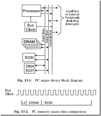
The PC ‘‘core’’ circuitry consists of the microprocessor, memory, the interrupt controller and a DMA controller, as shown in Fig. 13-1. This set of hardware can run any program or interface with hardware attached to this ‘‘local bus’’. While you may think of processor memory in terms of the megabytes that were advertised when you bought the PC, there are actually three different types of memory that are accessed.
The term ‘‘local memory’’ is kind of a loosely defined term that I use to describe memory on the PC’s motherboard and not on external cards or subsystems. There are a number of different kinds of memory used on the motherboard, each with a different set of characteristic features. The first type, ‘‘ROM’’ (‘‘Read Only Memory’’) is fairly slow and can only be read; it contains the PC start up (‘‘boot’’) code. Next, there is what I will call
‘‘main memory’’, which is measured in tens or hundreds of megabytes (and was prominently advertised when you bought your PC) and is moderately fast.
The PC’s processor itself has ‘‘cache memory’’ which runs at the processor’s speed and, ideally, all execution takes place from this area as this will help speed up the operation of the PC. Figure 13-2 shows the number of clock cycles for the different cases of the PC’s processor reading from cache memory (at full local bus clock speed), main memory (which has 50 ns access time DRAMs) and ROM (150 ns access time). The importance of being able to run entire applications from cache memory should be obvious to you.
‘‘DMA’’ stands for ‘‘Direct Memory Access’’ and consists of a hardware device that can be programmed to create addressing and control signals to move data between devices within the system without involving the processor. DMA is most typically used in the PC for moving data to and from the disk drives.
Interrupts are hardware events, passed to the ‘‘8237 interrupt controller’’ chip that requests the PC’s processor to stop what it is currently doing and respond to the external request. This request does not have to be responded to immediately and it is up to the programmer’s discretion to decide how to respond to the request.
All PC systems have multiple busses for system expansion and improved communications. Before going too much further, I should list the characteristics of what a computer bus is. A computer bus is defined as having:
1. A method for the controlling microprocessor to provide addresses bus hardware for both memory and I/O access.
2. The ability of the cards to request interrupt and DMA processing by the controlling microprocessor.
3. The ability to enhance the operation of the PC.
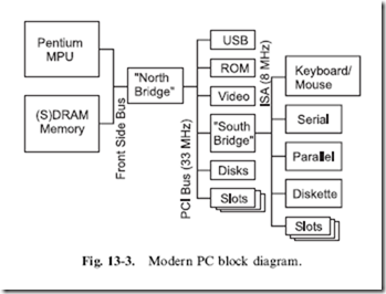
In a modern PC, there are usually three primary busses, each one delineated by the access speed they are capable of running at and the devices normally attached to them (see Fig. 13-3). The three busses have evolved over time to provide data rates consistent for the needs of the different devices. You might consider that there is a problem with cause and effect, but the busses and devices attached to them have sorted themselves out over the years.
The ‘‘Front Side Bus’’ (usually referred to by its acronym ‘‘FSB’’) runs at a very high speed specific to the processor. This is used by the processor to access DRAM memory directly as well as provide an interface to the system peripherals.
The ‘‘PCI’’ (‘‘Personal Computer Interface’’) Bus. This bus is not only a staple of all modern PCs but is also available on many other system architectures as well. This allows PCI bus cards to be used across a number of
different systems and eliminates the need for designers and manufacturers to replicate their products for different platforms. PCI is somewhat of a ‘‘hybrid’’ bus, with some internal features of the PC (notably video and hard file controllers) using the PCI busses built into the copper traces on the motherboard as well as providing access to adapter cards in ‘‘slots’’. PCI is notoriously difficult to create expansion cards for. Along with the fairly high data rate speed (33 and 66 MHz), there are data transfer protocols which generally require an ASIC to decode and process bus requests.
The last bus interfaces the ‘‘legacy’’ interfaces of the PC together and is known as the ‘‘Industry Standard Architecture’’ (‘‘ISA’’) bus. This bus typically has a data transfer speed of 125 ns – the same as the original PC/AT.
When you are interfacing digital electronic devices to your PC, chances are the interface will be connected to this bus.
The Parallel (Printer) Port
When hardware is to be interfaced with the PC, often the first method chosen is the ‘‘Parallel’’ (Printer) port. If I was being introduced to the PC for the first time, I would probably look at this method first as well, but as I have learned more about the PC, using the parallel port would actually be one of the last methods that I would look at. The parallel port is really the most difficult interface in the PC to use because it is really device (printer) specific, has a limited number of I/O pins and is very difficult to time operations with accuracy. The only reason why I would see applications using a parallel port for interfacing is because, electronically, it does not need a level translator and can connect directly to TTL/CMOS logic.
In the 1970s, the Centronics Corporation developed a 25 pin ‘‘D-Shell’’ connector standard for wiring a computer to their printers. The early printer interfaces in the PC, after sending a byte, would wait for a handshaking line to indicate that the printer was ready for the next character before sending the next one. As you could imagine, this method was very slow and took up all the PC’s cycles in printing a file.
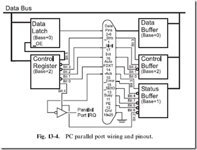
This ‘‘pinout’’ very quickly became a standard in the computer industry. This connector consisted of an eight-pin data output port with strobe, four control lines passed to the printer and five status lines from the printer, as shown in Fig. 13-4. By the time the PC was being developed, this interface was the de facto industry standard and was chosen by IBM to help make the PC an ‘‘Industry’’ standard. When the printer port for the PC was being
developed, little thought was given to enhancing the port beyond the then current standard level of functionality.
To improve the functionality of the printer port, IBM, when designing the PC/AT, changed the eight data bit output only circuitry to allow data bits to be output as well as read back. This was accomplished by using pulled up open collector outputs that were passed from the ‘‘Data Latch’’ of Fig. 13-4, to the 25 pin D-Shell connector and on to the ‘‘Data Buffer’’, which could read the eight bits and see if anything was changed.
When a read of the eight data bits takes place, the eight output bits should all be ‘‘High’’ to allow the parallel port’s pull ups and the open collector outputs of the peripheral device to change the state of the pins. The bi-directional data capability in the PC/AT’s parallel port allowed hardware to interface to the PC to be very easily designed. Further enhancing the ease in which devices could be designed to work with the parallel port was the standard timing provided by the PC/AT’s ISA bus and BIOS.
Surprisingly, given this background, the biggest problem today with interfacing to the parallel port is timing signals properly. Depending on the different PCs that I have experimented with, I have seen parallel I/O port read and write timings from about 700 ns to less than 100 ns. When you design your interface to the IBM PC, you can either ignore the actual timings of the parallel port and execute signals that are many milliseconds long, ‘‘tune’’ the code to the specific PC you are working with or add a time delay function, like a 555 wired as a monostable that the PC can poll from the printer port to properly time its I/O operations.
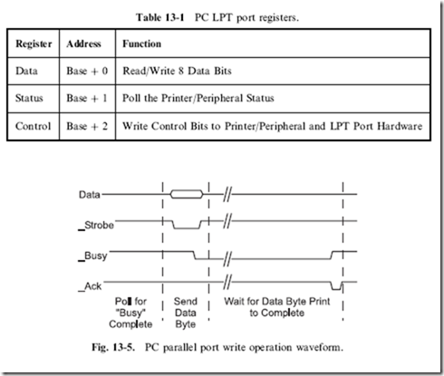
There are three registers that you will have to access from your PC program to control the parallel port. The ‘‘Control Register’’, provides an operating control to the external device as well as to the internal interrupt function of the parallel port. The ‘‘Status Buffer’’ is read to poll the status bits from the printer. The last register, called ‘‘Data’’, allows eight bits to be written or read back from the parallel port. Starting at a parallel port (known as ‘‘LPT’’ in the PC), the registers are addressed as shown in Table 13-1 relative to a ‘‘Base’’ address which is at 0x0378 and 0x0278 for ‘‘LPT1’’ and ‘‘LPT2’’, respectively.
When the parallel port passes data to a printer, the I/O pins create the basic waveform shown in Fig. 13-5. It is important to note that the Printer BIOS routines will not send a new character to the printer until it is no longer ‘‘Busy’’. When ‘‘Busy’’ is no longer active, the ‘‘Ack’’ line is pulsed active, which can be used to request an interrupt to indicate to data output code that
the printer is ready to accept another character. The timing of the circuit for printer applications is quite simple, with 0.5 ms minimum delays needed between edges on the waveforms in Fig. 13-5.
Video Output
The first computer CRT display was the ‘‘vector’’ display in which the ‘‘X-Y’’ deflection plates moved the electron beam to a desired location on the screen and then drew a line to the next location. This was repeated until the entire image was drawn on the screen (at which time the process started over). This was popular in early computers because only a modest amount of processing power and video output hardware was needed to draw simple graphics. Because of the way the vector displays operated, a complex image was often darker than and could ‘‘flash’’ more than a ‘‘raster’’ (TV-like) display because a simple image would require fewer vector ‘‘strokes’’ and could be refreshed more often. Vector displays enjoyed some popularity in early computer video displays (including video games), but really haven’t been used at all for over 10 years.
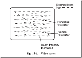
Today, a more popular method of outputting data from a computer is to use a ‘‘raster’’ display, in which an electron beam is drawn across the cathode ray tube in a regular, left to right, up and down, pattern. When some detail of the image is to be drawn on the screen, the intensity of the beam is increased when the beam passes a particular location on the screen, which causes the phosphors to glow more brightly, as shown in Fig. 13-6. If you have an old
black and white TV (or monochrome computer monitor), chances are you can increase the ‘‘brightness’’/‘‘contrast’’ controls on a dark signal to see the different features I’ve shown above.
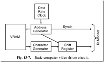
All raster computer output hardware consists of a shift register fed by data from a ‘‘Video RAM’’ (‘‘VRAM’’). In Fig. 13-7, the data to be output is read from the VRAM and then passed to a character generator, which converts the data from the Video RAM into a series of dots appropriate for the character. This series of dots is then shifted out to the hardware that drives the raster on the video monitor. If graphical data is output, then the ‘‘Character Generator’’ is not needed in the circuit and the output from the VRAM is passed directly to the shift register. The shift register may also be connected to a ‘‘DAC’’ (‘‘Digital Analog Converter’’), which converts the digital data into a series of analog voltages that display different intensities of color on the display.
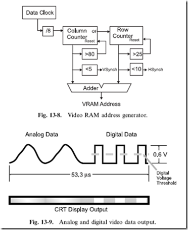
The addresses for each byte’s data to be transferred to the display are accomplished by using an ‘‘Address Generator’’, which controls the operation of the display (Fig. 13-8). The Address Generator divides the ‘‘data rate’’ (the number of ‘‘pixels’’ displayed per second on the screen) into character-sized ‘‘chunks’’ for shifting out, resets address counters when the end of the line is encountered and also outputs ‘‘Synch’’ information for the monitor to properly display data on the screen.
The circuit in Fig. 13-8 shows an example address generator for an 80 character by 25-row display. This circuit resets the counters when the end of the line and ‘‘field’’ (end of the display) is reached. At the start of the line and ‘‘field’’, horizontal and vertical synch information is sent to the monitor so the new field will line up with the previous one.
I have presented this information on standard video inputs to give you some background on how ‘‘NTSC’’ televisions work and what their input
signals look like. ‘‘NTSC’’ is the television ‘‘composite video’’ standard for North America and is an acronym for the ‘‘National Television Standards Council’’, the governing body put in place for television in the United States in the 1940s (today, television broadcasting technical standards are controlled by the Federal Communications Commission or FCC).
‘‘Composite NTSC’’ is the signal typically received by your TV set and
consists of both the data input streams along with the formatting information (called synchronization or synch pulses) that are used by the TV set to recognize where the incoming signal is to be placed on the screen. The incoming data, shown in Fig. 13-9 consists of voltage levels (from 0 to
0.6 volts) varying over time. This data is wiped across the CRT from left to right as a single line raster.
On the left-hand side of the incoming serial data shown in Fig. 13-9, I have drawn the data as a typical, analog video stream. The analog voltage levels are used to control the output level of the electron ‘‘gun’’ in the CRT: the higher the input voltage level, the brighter the output on the current raster of the CRT display, as shown at the bottom of the diagram. To the right of the analog data of Fig. 13-9, I have drawn some signals that jump from 0 volts to 0.6 volts and back again. This section of the raster is labeled as ‘‘Digital Data’’. I call this digital data because it is either all on or all off and it can be read as data by simply comparing whether the data is above or below the ‘‘threshold’’ marked on Fig. 13-9.
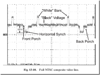
The start of each new line is specified by the inclusion of a ‘‘horizontal synch pulse’’ (‘‘hsynch’’), as shown in Fig. 13-10. This pulse is differentiated from the serial data by being at a voltage level less than the ‘‘black’’ level – this is where the term ‘‘blacker than black’’ comes from. Before and after the synch pulse, there are two slightly negative voltage regions called the ‘‘front porch’’ and ‘‘back porch’’, respectively. The front porch is 1.4 ms long, the back porch and horizontal synch pulse are 4.4 ms each. The entire line is 63.5 ms in length, and when you take away the 10.2 ms of horizontal synch information, you are left with 53.3 ms per line for the analog or digital data.
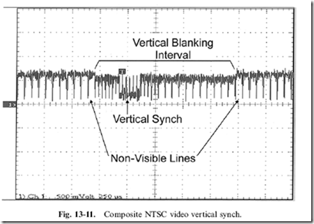
There are 262 or 263 lines of data sent to the TV, with the first 12 normally being at the -0.08 volt ‘‘porch’’ level and called the ‘‘vertical blanking interval’’. I say it is normally at the -0.08 volt porch level, except when ‘‘closed captioning’’ information is available. Closed captioning, as I’m sure
you are aware, is the text that comes on the screen to allow hearing impaired
people to watch TV. When closed captioning data is included in the vertical blanking interval, digital pulses, similar to the ones shown in Fig. 13-11 are built into each line and decoded by circuitry built into the TV.
The TV set does not have a counter built into it to indicate when the CRT’s gun should reset and go back to the top of the screen. Instead the incoming signal indicates when a vertical retrace must take place by its inclusion of a ‘‘vertical synchronization pulse’’ (‘‘vsynch’’). The oscilloscope picture (Fig. 13-11) shows what the vertical synch pulse looks like: it is actually a series of half-sized lines followed by a number of inverted half- sized lines.
So far, I have described NTSC video as having 262 or 263 lines, but if you look at the specifications for a TV set, you will see that it can accept 525 lines of NTSC data. A full NTSC screen consists of two ‘‘fields’’ of data: one 262 lines in size and the other 263 lines. The fields are offset by one half the width of a line – after the first field is displayed, the second fills in the spaces between the lines displayed by the first field. This is called ‘‘interlacing’’ the two fields together into a single ‘‘frame’’.
With the information contained within this section, you have enough information to create a monochrome video output circuit. I’ve done it a number of times with basic microcontrollers; as long as you keep your field width, vertical and horizontal synch pulses timed consistently, you will find that you can build your own composite video output display that you can send to an old TV. Even though with the information contained here, you should be able to design an NTSC composite video output perfectly, I still don’t recommend trying it out on the family’s good TV.
