INTEL 8086 : Introduction , 8086 Main Memory and 8086 Registers

clip_image001INTEL 8086

This chapter covers the Intel8086 in detail. Intel’s 32-bit microprocessors are based on the Intel 8086. Therefore, the 8086 provides an excellent educational tool for understanding Intel 32- and 64-bit microprocessors. Because the 8086 and its peripheral chips are inexpensive, the implementation costs of 8086-based systems are low. This makes the 8086 appropriate for thorough coverage in a first course on microprocessors. Thus, the 8086 is covered in detail in this chapter.

9.1 Introduction

The 8086 was Intel’s first 16-bit microprocessor. This means that the 8086 has a 16-bit ALU. The 8086 contains 20 address pins. Therefore, it has a main (directly addressable) memory of one megabyte (220 bytes).

The memory of an 8086-based microcomputer is organized as bytes. Each byte is uniquely addressed with 20-bit addresses of 00000 16,00001 16, ••• FFFFF 16• An 8086 word in memory consists of any two consecutive bytes; the low-addressed byte is the low byte of the word and the high-addressed byte contains the high byte as follows:

imageThe 16-bit word at the even address 02000 16 is A102 16• Next, consider a word stored at an address 30151 16 as follows:

imageThe 16-bit word stored at the odd address 30151 16 is 462E 16.

The 8086 always reads a 16-bit word from memory. This means that a word instruction

accessing a word starting at an even address can perform its function with one memory read. A word instruction starting at an odd address, however, must perform two memory accesses to two consecutive memory even addresses, discarding the unwanted bytes of each. For byte read starting at odd address N, the byte at the previous even address N- I is also accessed but discarded. Similarly, for byte read starting at even address N, the byte with odd address N + 1 is also accessed but discarded.

For the 8086, register names followed by the letters X, H, or L in an instruction for data transfer between register and memory specify whether the transfer is 16-bit or 8- bit. For example, consider MOV AX, (START]. If the 20-bit address START is an even number such as 02212 16, then this instruction loads the low (AL) and high (AH) bytes of

the 8086 16-bit register AX with the contents of memory locations 02212 16 and 02213 16, respectively, in a single access. Now, if START is an odd number such as 0221316, then the MOV AX, [ START ] instruction loads AL and AH with the contents of memory locations 02213 16 and 02214 16, respectively, in two accesses. The 8086 also accesses memory

locations 02212 16 and 02215 16 but ignores their contents.

Next,considerMOV AL, [START]. IfSTARTisanevennumbersuchas30156 16, then this instruction accesses both addresses, 30156 16 and 30157 16, but loads AL with the contents of 30156 16 and ignores the contents of 30157 16• However, if START is an odd number such as 30157 16, then MOV AL, [START] loads AL with the contents of 3015716• In this case the 8086 also reads the contents of30156 16 but discards it.

The 8086 is packaged in a 40-pin chip. A single +5 V power supply is required.

The clock input signal is generated by the 8284 clock generator/driver chip. Instruction execution times vary between 2 and 30 clock cycles.

There are four versions of the 8086. They are 8086, 8086-1, 8086-2, and 8086-4. There is no difference between the four versions other than the maximum allowed clock speeds. The 8086 can be operated from a maximum clock frequency of 5 MHz. The maximum clock frequencies of the 8086-1, 8086-2 and 8086-4 are 10 MHz, 8 MHz and 4 MHz, respectively.

The 8086 family consists of two types of 16-bit microprocessors, the 8086 and 8088. The main difference is how the processors communicate with the outside world. The 8088 has an 8-bit external data path to memory and 110; the 8086 has a 16-bit external data path. This means that the 8088 will have to do two READ operations to read a 16-bit word from memory. Similarly, two write operations are required to write a 16-bit word into memory. In most other respects, the processors are identical. Note that the 8088 accesses memory in bytes. No alterations are needed to run software written for one microprocessor on the other. Because of similarities, only the 8086 will be considered here. The 8088 was used in designing IBM’s first personal computer.

An 8086 can be configured as a small uniprocessor (minimum mode when the MN/MX pin is tied to HIGH) or as a multiprocessor system (maximum mode when the MN/MX pin is tied to LOW). In a given system, the MN/MX pin is permanently tied to either HIGH or LOW. Some of the 8086 pins have dual functions depending on the selection of the MN/MX pin level.

In the minimum mode (MN/MX pin HIGH), these pins transfer control signals directly to memory and I/0 devices; in the maximum mode (MN/MX pin LOW), these same pins have different functions that facilitate multiprocessor systems. In the maximum mode, the control functions normally present in minimum mode are assumed by a support chip, the 8288 bus controller.

Due to technological advances, Intel introduced the high-performance 80186 and 80188, which are enhanced versions of the 8086 and 8088, respectively. The 8-MHz 80186/80188 provides two times greater throughput than the standard 5-MHz 8086/8088. Both have integrated several new peripheral functional units, such as a DMA controller, a 16-bit timer unit, and an interrupt controller unit, into a single chip. Just like the 8086 and 8088, the 80186 has a 16-bit data bus and the 80188 has an 8-bit data bus; otherwise, the architecture and instruction set of the 80186 and 80188 are identical. The 80186/80188 has an on-chip clock generator so that only an external crystal is required to generate the clock. The 80186/80188 can operate at either a 6- or an 8-MHz internal clock frequency. The crystal frequency is divided by 2 internally. In other words, external crystals of 12or 16 MHz must be connected to generate the 6- or 8-MHz internal clock frequency. The 80186/80188 is fabricated in a 68-pin package. Both processors have on-chip priority interrupt controller circuits to provide five interrupt pins. Like the 8086/8088, the 80186/80188 can directly address one megabyte of memory. The 80186/80188 is provided with 10 new instructions beyond the 8086/8088 instruction set. Examples of these instructions include INS and OUTS for inputting and outputting a string byte or string word.

The 80286, on the other hand, has added memory protection and management capabilities to the basic 8086 architecture. An 8-MHz 80286 provides up to 6 times greater throughput than the 5-MHz 8086. The 80286 is fabricated in a 68-pin package. The 80286 can be operated at a clock frequency of 4, 6, or 8 MHz. An external 82284 clock generator chip is required to generate the clock. The 82284 divides the external clock by 2 to generate the internal clock. The 80286 can be operated in two modes, real address and protected virtual address. Real address mode emulates a very high-performance 8086. In this mode, the 80286 can directly address one megabyte of memory. In virtual address mode, the 80286 can directly address 16 megabytes of memory. Virtual address mode provides (in addition to the real address mode capabilities) virtual memory management as well as task management and protection. The programmer can select one of these modes by loading appropriate data in the 16-bit machine status word (MSW) register by using the load instruction (LMSW).

The 80286 was used as the microprocessor of the IBM PC/AT personal computer.

An enhanced version of the 80286 is the 32-bit 80386 microprocessor. The 80386 was used as the microprocessor in the IBM 386PC. The 80486 is another 32-bit microprocessor. It is based on the Intel 80386 and includes on-chip floating-point circuitry. IBM’s 486 PC contains the 80486 chip. Other 32-bit and 64-bit Intel microprocessors include Pentium, Pentium Pro, Pentium II, Celeron, Pentium III, Pentium 4 and Merced.

Although the 8086 seems to be obsolete, it is expected to be around for some time from second sources. Therefore, a detailed coverage of the 8086 is included. A summary of the 32- and 64-bit microprocessors is then provided.

9.2 8086 Main Memory

The 8086 uses a segmented memory. There are some advantages to working with the segmented memory. First, after initializing the 16-bit segment registers, the 8086 has to deal with only 16-bit effective addresses. That is, the 8086 has to manipulate and store 16-bit address components. Second, because of memory segmentation, the 8086 can be effectively used in time-shared systems. For example, in a time-shared system, several users may share one 8086. Suppose that the 8086 works with one user’s program for, say, 5 milliseconds. After spending 5 milliseconds with one of the other users, the 8086 returns to execute the first user’s program. Each time the 8086 switches from one user’s program to the next, it must execute a new section of code and new sections of data. Segmentation makes it easy to switch from one user program to another.

The 8086’s main memory can be divided into 16 segments of 64K bytes each (16 x 64 KB = 1 MB). A segment may contain codes or data. The 8086 uses 16-bit registers to address segments. For example, in order to address codes, the code segment register must be initialized in some manner (to be discussed later): A 16-bit 8086 register called the "instruction pointer" (IP), which is similar to the program counter of a typical microprocessor, linearly addresses each location in a code segment. Because the size of the IP is 16 bits, the segment size is 64K bytes (216 . Similarly, a 16-bit data segment register must be initialized to hold the segment value of a data segment. The contents of certain 16-bit registers are designed to hold a 16-bit address in a 64-Kbyte data segment. One of these address registers can be used to linearly address each location once the data segment is initialized by an instruction. Finally, in order to access the stack segment, the 8086 16-bit stack segment (SS) register must be initialized; the 64-Kbyte stack is addressed linearly by a 16-bit stack pointer register. Note that the stack memory must be a read/write (RAM) memory. Whenever the programmer reads from or writes to the 8086 memory or stack, two components of a memory address must be considered: a segment value and, an address or an offset or a displacement value. The 8086 assembly language program works with these two components while accessing memory. These two 16-bit components (the contents of a 16-bit segment register and a 16-bit offset or IP) form a logical address. The programmer writes programs using these logical addresses in assembly language programming.

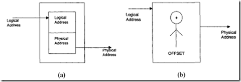
The 8086 includes on-chip hardware to map or translate these two 16-bit  components of a memory address into a 20-bit address called a "physical address" by shifting the contents of a segment register four times to left and then adding the contents of IP or offset. Note that the 8086 contains 20 address pins, so the physical address size is 20 bits wide.

Consider, for example, a logical address with the 16-bit code segment register contents of 2050 16 and the 16-bit 8086 instruction pointer containing a value of 0004w Suppose that the programmer writes an 8086 assembly language program using this logical address. The programmer assembles this program and obtains the object or machine code. When the 8086 executes this program and encounters the logical address, it will generate the 20-bit physical address as follows: If 16-bit contents of IP = 000416, 16-bit contents of code segment = 205016, 16-bit contents of code segment value after shifting logically 4 times to the left = 20500 16, then the 20-bit physical address generated by the 8086 on its 20-pin address is 20504 16 • Note that the 8086 assigns the low address to the low byte of a 16-bit register and the high address to the high byte of the 16-bit register for 16-bit transfers between the 8086 and main memory. This is called Little-endian byte ordering.

9.3 8086 Registers

As mentioned in Chapter 6, the 8086 is divided internally into two independent units: the bus interface unit (BIU) and the execution unit (EU). The BIU reads (fetches) instructions, reads operands, and writes results. The EU executes instructions already fetched by the BIU. The 8086 prefetches up to 6 instruction bytes from external memory into a FIFO (first-in-first-out) memory in the BIU and queues them in order to speed up instruction execution. The BIU contains a dedicated adder to produce the 20-bit address. The bus control logic of the BIU generates all the bus control signals, such as the READ and WRITE signals, for memory and 1/0. The BIU also has four 16-bit segment registers: the code segment (CS), data segment (DS), stack segment (SS), and extra segment (ES) registers.

All program instructions must be located in main memory, pointed to by the 16- bit CS register with a 16-bit offset contained in the 16-bit instruction pointer (IP). Note that immediate data are considered as part of the code segment. The SS register points to the current stack. The 20-bit physical stack address is calculated from the SS and SP (stack pointer) for stack instructions such as PUSH and POP. The programmer can create a programmer’s stack with the BP (base pointer) instead of the SP for accessing the stack using the based addressing mode. In this case, the 20-bit physical stack address is calculated from the BP and SS. The DS register points to the current data segment; operands for most instructions are fetched from this segment. The I6-bit contents of a register such as the SI (source index) or DI (destination index) or a I6-bit displacement are used as offsets for computing the 20-bit physical address.

The ES register points to the extra segment in which data (in excess of 64 KB pointed to by the DS) is stored. String instructions always use the ES and DI to determine the 20-bit physical address for the destination.

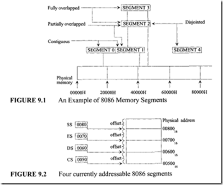
The segments can be contiguous, partially overlapped, fully overlapped, or disjointed. An example ofhow five segments (SEGMENT 0 through SEGMENT 4), may be stored in physical memory is shown in Figure 9.1. In this example, SEGMENTs 0 and I are contiguous (adjacent), SEGMENTs I and 2 are partially overlapped, SEGMENTs 2 and 3 are fully overlapped, and SEGMENTs 2 and 4 are disjointed.

Every segment must start on I6-byte memory boundaries. Typical examples of values of segments should then be selected based on physical addresses starting at 00000 16, 00010 16,00020 16, 00030 16, ••• , FFFF0 16• A physical memory location may be mapped into (contained in) one or more logical segments. Many applications can be written to simply initialize the segment registers and then forget them.

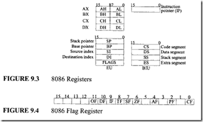
A segment can be pointed to by more than one segment register. For example, the DS and ES may point to the same segment in memory if a string located in that segment is used as a source segment in one string instruction and a destination segment in another string instruction. Note that, for string instructions, a destination segment must be pointed to by the ES. One example of four currently addressable segments is shown in Figure 9.2.

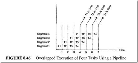
The EU decodes and executes instructions. It has a 16-bit ALU for performing arithmetic and logic operations. The EU has nine 16-bit registers: AX, BX, CX, DX, SP,
imageBP, SI, and DI, and the flag register. The 16-bit general registers AX, BX, ex, and DX can be used as two 8-bit registers (AH, AL; BH, BL; eH, eL; DH, DL). For example, the 16- bit register DX can be considered as two 8-bit registers DH (high byte ofDX) and DL (low byte of DX). The general-purpose registers AX, BX, ex, and DX perform the following functions:

  • The AX register is 16 bit wide whereas AH and AL are 8 bit wide. The use of AX and AL registers is assumed by some instructions. The I/0 (IN or OUT) instructions always use the AX or AL for inputting/outputting 16- or 8-bit data to or from an I/0 port. Multiplication and division instructions also use the AX orAL.
  • The BX register is called the "base register." This is the only general-purpose register whose contents can be used for addressing 8086 memory. All memory references utilizing this register content for addressing use the DS as the default segment register.
  • The ex register is known as the counter register because some instructions, such as SHIFT, ROTATE, and LOOP, use the contents of eX as a counter, For example, the instruction LOOP START will automatically decrement eX by 1 without affecting flags and will check to see if (ex) = 0. If it is zero, the 8086 executes the next instruction; otherwise, the 8086 branches to the label START.
  • The DX register, or data register, is used to hold the high 16-bit result (data) (LOW 16-bit data is contained in AX) after 16 x 16 multiplication or the high 16-bit dividend (data) before a 32 + 16 division and the 16-bit remainder after the division (16-bit quotient is contained in AX).
  • The two pointer registers, SP (stack pointer) and BP (base pointer), are used to access data in the stack segment. The SP is used as an offset from the current SS during execution of instructions that involve the stack segment in external memory. The SP contents are automatically updated (incremented or decremented) due to execution of a POP or PUSH instruction. The BP contains an offset address in the current SS. This offset is used by instructions utilizing the based addressing mode.
  • The two index registers, SI (source index) and DI (destination index), are used in indexed addressing. Note that instructions that process data strings use the SI and DI index registers together with the DS and ES, respectively, in order to distinguish between the source and destination addresses.
  • The flag register in the EU holds the status flags, typically after an ALU operation. The
imageEU sets or resets these flags to reflect the results of arithmetic and logic operations.

Figure 9.3 depicts the 8086 registers. It shows the nine 16-bit registers in the EU. As described earlier, each one of the AX, BX, CX, and DX registers can be used as two 8-bit registers or as one 16-bit register. The other registers can be accessed as 16- bit registers. Also shown are the four 16-bit segment registers and the 16-bit IP in the BIU. The IP is similar to the program counter. The CS register points to the current code segment from which instructions are fetched. The effective address is derived from the CS and IP. The SS register points to the current stack. The effective address is obtained from the SS and SP. The DS register points to the current data segment. The ES register points to the current extra segment where data is usually stored.

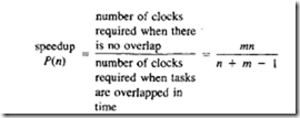
Figure 9.4 shows the 8086 flag register. The 8086 has six one-bit status flags. Let us now explain these flags.

  • AF (auxiliary carry flag) is set if there is a carry due to addition of the low nibble into the high nibble or a borrow due to the subtraction of the low nibble from the high nibble of a number. This flag is used by BCD arithmetic instructions; otherwise, AF is zero.
  • CF (carry flag) is set if there is a carry from addition or a borrow from subtraction.
  •  OF (overflow flag) is set if there is an arithmetic overflow (i.e., if the size of the result exceeds the capacity of the destination location). An interrupt on overflow instruction is available to generate an interrupt in this situation; otherwise, it is zero.
  •  SF (sign flag) is set if the most significant bit of the result is one; otherwise, it is zero.
  •  PF (parity flag) is set if the result has even parity; PF is zero for odd parity of the result.
  • ZF (zero flag) is set if the result is zero; ZF is zero for a nonzero result.

The 8086 has three control bits in the flag register that can be set or cleared by the programmer:

1. Setting DF (direction flag) causes string instructions to auto-decrement; clearing DF causes string instructions to auto-increment.

2. Setting IF (interrupt flag) causes the 8086 to recognize external maskable

interrupts; clearing IF disables these interrupts.

3. Setting TF (trap flag) puts the 8086 in the single-step mode. In this mode, the 8086 generates an internal interrupt after execution of each instruction. The user can write a service routine at the interrupt address vector to display the desired registers and memory locations. The user can thus debug a program.
 

Pipeline Processing , Basic Concepts , Arithmetic Pipelines and Instruction Pipelines

8.4.2 Pipeline Processing

The purpose of this section is to provide a brief overview of pipelining.

Basic Concepts

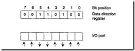
Assume a task T is carried out by performing four activities: AI, A2, A3, and A4, in that order. Hardware Hi is designed to perform the activity Ai. Hi is referred to as a segment, and it essentially contains combinational circuit elements. Consider the arrangement shown in Figure 8.45.

In this configuration, a latch is placed between two segments so the result computed

by one segment can serve as input to the following segment during the next clock period. The execution of four tasks Tl, T2, T3, and T4 using the hardware of Figure 8.45 is described using a space-time chart shown in Figure 8.46.

Initially, task Tl is handled by segment I. After the first clock, segment 2 is busy with Tl

while segment 1 is busy with T2. Continuing in this manner, the task Tl is completed at the end of the fourth clock. However, following this point, one task is shipped out per clock. This is the essence of the pipeline concept. A pipeline gains efficiency for the same reason as an assembly line does: Several activities are performed but not on the same material. Suppose ti and L denote the propagation delays of segment i and the latch, respectively. Then the pipeline clock period T can be expressed as follows:

T = max (Tl, T2, … Tn) + L

The segment with the maximum delay is known as the bottleneck, and it decides the pipeline clock period T. The reciprocal ofT is referred to as the pipeline frequency.

Consider the execution of m tasks using an n-segment pipeline. In this case, the

image

first task will be completed after n clocks (because there are n segments) and the remaining m-1 tasks are shipped out at the rate of one task per pipeline clock.

Therefore, n + (m – 1) clock periods are required to complete m tasks using an n-s egment pipeline. If all m tasks are executed without any overlap, mn clock periods are needed because each task has to pass through all n segments. Thus speed gained by an n segment pipeline can be shown as follows:

image

P(n) approaches n when m approaches infinity. This implies that when a large number of tasks are carried out using ann-segment pipeline, ann-fold increase in speed can be expected.

The previous result shows that the pipeline completes m tasks in the m + n – 1 clock periods. Therefore, its throughput can be defined as follows:

image

For a large value of m, U(n) approaches 1/T, which is the pipeline frequency. Thus the throughput of an ideal pipeline is equal to the reciprocal of its clock period. The efficiency of an n-segment pipeline is defined as the ratio of the actual speedup to the maximum speedup realized.

image

This illustrates that when m is very large, E(n) approaches 1 as expected.

In many modem computers, the pipeline concept is used in carrying out two tasks: arithmetic operations and instruction execution.

Arithmetic Pipelines

The pipeline concept can be used to build high-speed multipliers. Consider the multi­ plication P = M * Q, where M and Q are 8-bit numbers. The 16-bit product P can be expressed as:

image

where, S; = Mq;2; and each S; represents a 16-bit partial product. Each partial product is the shifted multiplicand. All 8 partial products can be added using several carry-save adders.

This concept can be extended to design an n x n pipelined multiplier. Here n partial products must be summed with 2n bits per partial product. So, as n increases, the hardware cost associated with a fully combinational multiplier increases in an exponential fashion. To reduce the hardware cost, large multipliers are designed.

The pipeline concept is widely used in designing floating-point arithmetic units. Consider the process of adding two floating point numbers A= 0.9234 * I 04 and B = 0.48 * 102 • First, notice that the exponents of A and Bare unequal. Therefore, the smaller number should be modified so that its exponent is equal to the exponent of the greater number.

For this example, modify B to 0.0048 * 104• This modification step is known as exponent alignment. Here the decimal point of the significand 0.48 is shifted to the right to obtain the desired result. After the exponent alignment, the significands 0.9234 and 0.0048 are added to obtain the final solution of0.9282 * 104

For a second example, consider the operation A- B, where A= 0.9234 * 104 and B = 0.9230 * 104• In this case, no exponent alignment is necessary because the exponent of A equals to the exponent of B. Therefore, the significand of B is subtracted from the significand of A to obtain 0.9234- 0.9230 = 0.0004. However, 0.0004 * 104 cannot be the final answer because the significand, 0.0004, is not normalized. A floating-point number with base b is said to be normalized if the magnitude of its significand satisfies the following inequality: 1/b lsignificandl < 1.

In this example, since b = 10, a normalized floating-point number must satisfy the condition:

0.1 lsignificandl < I

(Note that normalized floating-point numbers are always considered because for each real­ world number there exists one and only one floating-point representation. This uniqueness property allows processors to make correct decisions while performing compare operations).

The final answer is modified to 0.4 * 101 • This modification step is known as postnormalization, and here the significand is shifted to the left to obtain the correct result.

In summary, addition or subtraction of two floating-point numbers calls for four activities:

I. Exponent comparison

2. Exponent alignment

3. Significand addition or subtraction

4. Postnormalization

image

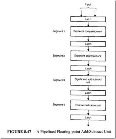
Based on this result, a four-segment floating-point adder/subtracter pipeline can be built, as shown in Figure 8.47.

It is important to realize that each segment in this pipeline is primarily composed of combinational components such as multiplexers. The shifter used in this system is the barrel shifter discussed earlier. Modem microprocessors such as Motorola MC 68040 include a 3-stage floating-point pipeline consisting of operand conversion, execute, and result normalization.

Instruction Pipelines

Modem microprocessors such as Motorola MC 68020 contain a 3-stage instruction pipeline. Recall that an instruction cycle typically involves the following activities:

I. Instruction fetch

2. Instruction decode

3. Operand fetch

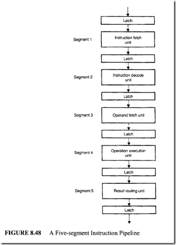
4. Operation execution 5. Result routing.

This process can be effectively carried out by using the pipeline shown in Figure 8.48. As mentioned earlier, in such a pipelined scheme the first instruction requires five clocks to complete its execution. However, the remaining instructions are completed at a rate of one per pipeline clock. Such a situation prevails as long as all the segments are busy.

In practice, the presence of branch instructions and conflicts in memory accesses poses a great problem to the efficient operation of an instruction pipeline.

image


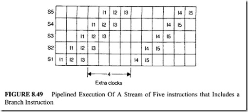
imageFor example, consider the execution of a stream of five instructions: I1, 12, 13, 14, and IS in which I3 is a conditional branch instruction. This stream is processed by the instruction pipeline (Figure 8.48) as depicted in Figure 8.49.

When a conditional branch instruction is fetched, the next instruction cannot be

fetched because the exact target is not known until the conditional branch instruction has been executed. The next fetch can occur once the branch is resolved. Four additional clocks are required due to 13.

Suppose a stream of s instructions is to be executed using an n-segment pipeline. If c is the probability for an instruction to be a conditional branch instruction, there will be s c conditional branch instructions in a stream of s instructions. Since each branch instruction requires n – I additional clocks, the total number of clocks required to process a stream of s instructions is

image

For no conditional branch instructions (c = 0), 5 instructions per instruction cycle are executed. This is the best result produced by a five-segment pipeline. If 25% of the

image

image

per instruction cycle can be executed. This shows how pipeline efficiency is significantly decreased even with a small percentage of branch instructions.

·In many contemporary systems, branch instructions are handled using a strategy called Target Prefetch. When a conditional branch instruction is recognized, the immediate successor of the branch instructions and the target of the branch are prefetched. The latter is saved in a buffer until the branch is executed. If the branch condition is successful, one pipeline is still busy because the branch target is in the buffer.

Another approach to handle branch instructions is the use of the delayed branch concept. In this case, the branch does not take place until after the following instruction. To illustrate

image

image

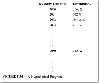
this, consider the instruction sequence shown in Figure 8.50.

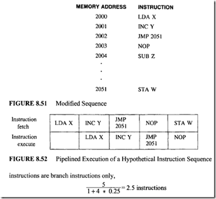
Suppose the compiler inserts a NOP instruction and changes the branch instruction to JMP 2051. The program semantics remain unchanged. This is shown in Figure 8.51.

This modified sequence depicted in Figure 8.51 will be executed by a two-segment pipeline, as shown in Figure 8.52:

  • Instruction fetch
  • Instruction execute

Because of the delayed branch concept, the pipeline still functions correctly without damage.

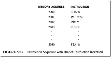
The efficiency of this pipeline can be further improved if the compiler produces a new sequence as shown in Figure 8.53.

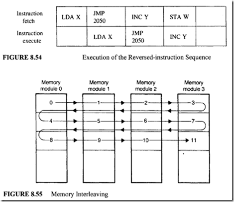
In this case, the compiler has reversed the instruction sequence. The JMP instruction is placed in the location 2001, and the INC instruction is moved to memory location 2002. This reversed sequence is executed by the same 2-segment pipeline, as shown in Figure 8.54.

It is important to understand that due to the delayed branch rule, the INC Y instruction is fetched before the execution of JMP 2050 instruction; therefore, there is no change in the order of instruction execution. This implies that the program will still produce the same result. Since the NOP instruction was eliminated, the program is executed more efficiently.

The concept of delayed branch is one of the key characteristics of RISC as it makes concurrency visible to a programmer.

As does the presence of branch instructions, memory-access conflicts cause damage to pipeline performance. For example, if the instructions in the operand fetch and result-saving units refer to the same memory address, these operations cannot be overlapped.

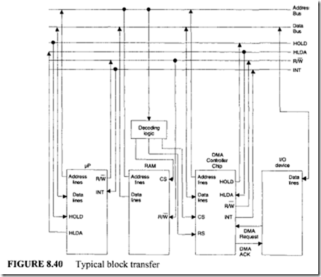
To reduce such memory conflicts, a new approach called memory interleaving is often employed. For this case, the memory addresses are distributed among a set of memory modules, as shown in Figure 8.55.

In this arrangement, memory is distributed among many modules. Since consecutive addresses are placed into different modules, the CPU can access several words in one memory access.


Direct Memory Access (DMA) , Summary of I/O , Fundamentals of Parallel Processin and General Classifications of Computer Architectures

8.2.3 Direct Memory Access (DMA)

Direct memory access (DMA) is a technique that transfers data between a microcomputer’s memory and an I/O device without involving the microprocessor. DMA is widely used in transferring large blocks of data between a peripheral device such as a hard disk and the microcomputer’s memory. The DMA technique uses a DMA controller chip for the data­ transfer operations. The DMA controller chip implements various components such as a counter containing the length of data to be transferred in hardware in order to speed up data transfer. The main functions of a typical DMA controller are summarized as follows:

  • The I/O devices request DMA operation via the DMA request line of the controller chip. The controller chip activates the microprocessor HOLD pin, requesting the microprocessor to release the bus.
  • The processor sends HLDA (hold acknowledge) back to the DMA controller, indicating that the bus is disabled. The DMA controller places the current value of its internal registers, such as the address register and counter, on the system bus and sends a DMA acknowledge to the peripheral device. The DMA controller completes the DMA transfer.

There are three basic types of DMA: block transfer, cycle stealing, and interleaved DMA. For block-transfer DMA, the DMA controller chip takes over the bus from the microcomputer to transfer data between the microcomputer memory and I/O device. The microprocessor has no access to the bus until the transfer is completed. During this time, the microprocessor can perform internal operations that do not need the bus. This method is popular with microprocessors. Using this technique, blocks of data can be transferred.

Data transfer between the microcomputer memory and an I/O device occurs on a word-by-word basis with cycle stealing. Typically, the microprocessor is generated by ANDing an INHIBIT signal with the system clock. The system clock has the same frequency as the microprocessor clock. The DMA controller controls the INHIBIT line. During normal operation, the INHIBIT line is HIGH, providing the microprocessor clock. When DMA operation is desired, the controller makes the INHIBIT line LOW for one clock cycle. The microprocessor is then stopped completely for one cycle. Data transfer

between the memory and I/O takes place during this cycle. This method is called "cycle stealing" because the DMA controller takes away or steals a cycle without microprocessor recognition. Data transfer takes place over a period of time.

With interleaved DMA, the DMA controller chip takes over the system bus when the microprocessor is not using it. For example, the microprocessor does not use the bus while incrementing the program counter or performing an ALU operation. The DMA controller chip identifies these cycles and allows transfer of data between the memory and I/O device. Data transfer takes place over a period of time for this method.

Because block-transfer DMA is common with microprocessors, a detailed

description is provided. Figure 8.40 shows a typical diagram of the block-transfer DMA. In the figure, the I/O device requests the DMA transfer via the DMA request line connected to the controller chip. The DMA controller chip then sends a HOLD signal to the microprocessor, and it then waits for the HOLD acknowledge (HLDA) signal from the microprocessor. On receipt of the HLDA, the controller chip sends a DMA ACK signal to the I/O device. The controller takes over the bus and controls data transfer between the RAM and I/O device. On completion of the data transfer, the controller interrupts the microprocessor by the INT line and returns the bus to the microprocessor by disabling the HOLD and DMA ACK signals.

The DMA controller chip usually has at least three registers normally selected

by the controller’s register select (RS) line: an address register, a terminal count register, and a status register. Both the address and terminal counter registers are initialized by the microprocessor. The address register contains the starting address of the data to be transferred, and the terminal counter register contains the desired block to be transferred. The status register contains information such as completion ofDMA transfer. Note that the

image

imageDMA controller implements logic associated with data transfer in hardware to speed up the DMA operation.

8.3 Summary of I/O

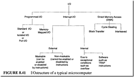
Figure 8.41 summarizes various 110 devices associated with a typical microprocessor.

8.4 Fundamentals of Parallel Processin :

The term "parallel processing" means improving the performance of a computer system by carrying out several tasks simultaneously. A high volume of computation is often required in many application areas, including real-time signal processing. A conventional single computer contains three functional elements: CPU, memory, and I/O. In such a uniprocessor system, a reasonable degree of parallelism was achieved in the following manner:

l. The IBM 370/168 and CDC 6600 computers included a dedicated I/O processor.

This additional unit was capable of performing all I/O operations by employing the DMA technique discussed earlier. In these systems, parallelism was achieved by keeping the CPU and I/O processor busy as much as possible with program execution and I/O operations respectively.

2. In the CDC 6600 CPU, there were 24 registers and 10 execution units. Each execution unit was designed for a specific operation such as addition, multiplication, and shifting. Since all units were independent of each other, several operations were performed simultaneously.

3. In many uniprocessor systems such as IBM 360, parallelism was achieved by using high-speed hardware elements such as carry-look-ahead adders and carry-save adders.

4. In several conventional computers, parallelism is incorporated at the instruction­ execution level. Recall that an instruction cycle typically includes activities such as op code fetch, instruction decode, operand fetch, operand execution, and result saving. All these operations can be carried out by overlapping the instruction fetch phase with the instruction execution phase. This is known as instruction pipelining. This pipelining concept is implemented in the state-of-the-art microprocessors such as Intel’s Pentium series.

5. In many uniprocessor systems, high throughput is achieved by employing high speed memories such as cache and associative memories. The use of virtual memory concepts such as paging and segmentation also allows one to achieve high processing rates because they reduce speed imbalance between a fast CPU and a slow periphal device such as a hard disk. These concepts are also implemented in today’s microprocessors to achieve high performance.

6. It is a common practice to achieve parallelism by employing software methods such as multiprogramming and time sharing in uniprocessors. In both techniques, the CPU is multiplexed among several jobs. This results in concurrent processing, which improves the overall system throughput.

8.4.1 General Classifications of Computer Architectures

Over the last two decades, parallel processing has drawn the attention of many research workers, and several high-speed architectures have been proposed. To present these results in a concise manner, different architectures must be classified in well defined groups.

All computers may be categorized into different groups using one of three classification methods:

1. Flynn

2.Feng

3. Handler

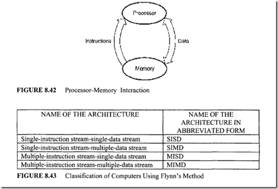
The two principal elements of a computer are the processor and the memory. A processor manipulates data stored in the memory as dictated by the instruction. Instructions are stored in the memory unit and always flow from memory to processor. Data movement

image

is bidirectional, meaning data may be read from or written into the memory. Figure 8.42 shows the processor-memory interaction.

The number of instructions read and data items manipulated simultaneously by the processor form the basis for Flynn’s classification. Figure 8.43 shows the four types of computer architectures that are defined using Flynn’s method. The SISD computers are capable of manipulating a single data item by executing one instruction at a time. The SISD classification covers the conventional uniprocessor systems such as the VAX-11, IBM 370, Intel 8085, and Motorola 6809. The processor unit of a SISD machine may have one or many functional units. For example, the VAX-11/780 is a SISD machine with a single functional unit. CDC 6600 and IBM 370/168 computers are typical examples of SISD systems with multiple functional units. In a SISD machine, instructions are executed in a strictly sequential fashion. The SIMD system allows a single instruction to manipulate several data elements. These machines are also called vector machines or array processors. Examples of this type of computer are the ILLIAC-IV and Burroughs Scientific Processor (BSP).

The ILLIAC- IV was an experimental parallel computer proposed by the University of Illinois and built by the Burroughs Corporation. In this system, there are 64 processing elements. Each processing element has its own small local memory unit. The operation of all the processing elements is under the control of a central control unit (CCU). Typically, the CCU reads an instruction from the common memory and broadcasts the same to all processing units so the processing units can all operate on their own data at the same time. This configuration is very useful for carrying out a high volume of computations that are encountered in application areas such as finite-element analysis, logic simulation, and spectral analysis. Modem microprocessors such as Intel Pentium II use the SIMD architecture.

By definition, MISD refers to a computer in which several instructions manipulate the same data stream concurrently. The notion of pipelining is very close to the MISD definition.

A set of instructions constitute a program, and a program operates on several data elements. MIMD organization refers to a computer that is capable of processing several programs simultaneously. MIMD systems include all multiprocessing systems. Based on the degree of processor interaction, multiprocessor systems may be further divided into two groups: loosely coupled and tightly coupled. A tightly coupled system has high interaction between processors. Multiprocessor systems with low interprocessor communications are referred to as loosely coupled systems.

In Feng’s approach, computers are classified according to the number of bits processed within a unit time. However, Handler’s classification scheme categorizes computers on the basis of the amount of parallelism found at the following levels:

  • CPU
  • ALU
  • Bit

A thorough discussion of these schemes is beyond the scope of this book. Since contemporary microprocessors such as Intel Pentium II use SIMD architechture, a basic coverage of SIMD is provided next. The SIMD computers are also called array processors. A synchronous array processor may be defined as a computer in which a set of identical processing elements act under the control of a master controller (MC). A command given by the MC is simultaneously executed by all processing elements, and a SIMD system is formed. Since all processors execute the same instruction, this organization offers a great

image

attraction for vector processing applications such as matrix manipulation.

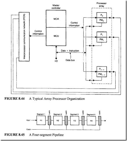
A conceptual organization of a typical array processor is shown in Figure 8.44. The Master Controller (MC) controls the operation of the processor array. This array consists ofN identical processing elements (P0 through Pn- 1). Each processing element P; is assumed to have its own memory, PMi, to store its data. The MC of Figure 8.44 contains two major components:

  • The master control unit (MCU)
  • The master control memory (MCM)

The MCU is the CPU of the master controller and includes an ALU and a set of registers. The purpose of the MCM is to hold the instructions and common data.

Each instruction of a program is executed under the supervision of the MCU in a sequential fashion. The MCU fetches the next instruction, and the execution of this instruction will take place in one of the following ways:

  • If the instruction fetched is a scalar or a branch instruction, it is executed by the MC itself.
  • If the instruction fetched is a vector instruction, such as vector add or vector multiply, then the MCU broadcasts the same instruction to each Pi, of the processor array, allowing all P;’s to execute this instruction simultaneously.

Assume the required data is already within the processing element’s private memory. Before execution of a vector instruction, the system ensures that appropriate data values are routed to each processing element’s private memory. Such an operation can be performed in two ways:

  • All data values can be transferred to the private memories from an external source via the system data bus.
  • The MCU can transfer the data values to the private memories via the control bus.

In an array processor like the one shown in Figure 8.44, it may be necessary to disable some processing elements during a vector operation. This is accomplished by including a mask register, M, in the MCU. The mask register contains a bit, m;, for each processing element, p;. A particular processing element, p;, will respond to a vector instruction broadcast by the MCU only when its mask bit, m;, is set to 1; otherwise, the processing element. P;, will not respond to the vector instruction and is said to be disabled.

In an array processor, it may be necessary to exchange data between processing elements. Such an exchange of data between processing elements takes place through the path provided by the interprocessor communication network (IPCN). Data exchanges refers to exchanges between scratchpad registers of the processing elements and exchanges between private memories of the processing elements.


Input/Output , Programmed I/O , Interrupt I/O , Interrupt Types , Interrupt Address Vector , Saving the Microprocessor Registers and Interrupt Priorities

8.2 Input/Output

One communicates with a microcomputer system via the I/O devices interfaced to it. The user can enter programs and data using the keyboard on a terminal and execute the programs to obtain results. Therefore, the I/O devices connected to a microcomputer system provide an efficient means of communication between the microcomputer and the outside world. These I/O devices are commonly called "peripherals" and include keyboards, CRT displays, printers, and disks.

The characteristics of the I/O devices are normally different from those of the microcomputer. For example, the speed of operation of the peripherals is usually slower than that of the microcomputer, and the word length of the microcomputer may be different from the data format of the peripheral devices. To make the characteristics of the I/O devices compatible with those of the microcomputer, interface hardware circuitry between the microcomputer and I/O devices is necessary. Interfaces provide all input and output transfers between the microcomputer and peripherals by using an I/O bus. An I/O bus carries three types of signals: device address, data, and command.

The microprocessor uses the I/O bus when it executes an I/O instruction. A typical I/O instruction has three fields. When the computer executes an I/O instruction, the control unit decodes the op-code field and identifies it as an I/O instruction. The CPU then places the device address and command from respective fields of the I/O instruction on the I/O bus. The interfaces for various devices connected to the I/O bus decode this address, and

an appropriate interface is selected. The identified interface decodes the command lines and determines the function to be performed. Typical functions include receiving data from an input device into the microprocessor or sending data to an output device from the microprocessor. In a typical microcomputer system, the user gets involved with two types of I/O devices: physical I/O and virtual I/O. When the computer has no operating system, the user must work directly with physical I/O devices and perform detailed I/O design.

There are three ways of transferring data between the microcomputer and physical I/O device:

I. Programmed I/O

2. Interrupt I/O

3. Direct memory access (DMA)

The microcomputer executes a program to communicate with an external device via a register called the "I/O port" for programmed I/O. An external device requests the microcomputer to transfer data by activating a signal on the microcomputer’s interrupt line during interrupt I/O. In response, the microcomputer executes a program called the interrupt-service routine to carry out the function desired by the external device. Data transfer between the microcomputer’s memory and an external device occurs without microprocessor involvement with direct memory access.

In a microcomputer with an operating system, the user works with virtual I/O devices. The user does not have to be familiar with the characteristics of the physical I/O devices. Instead, the user performs data transfers between the microcomputer and the physical I/O devices indirectly by calling the I/O routines provided by the operating system using virtual I/O instructions.

Basically, an operating system serves as an interface between the user programs and actual hardware. The operating system facilitates the creation of many logical or virtual I/O devices, and allows a user program to communicate directly with these logical devices. For example, a user program may write its output to a virtual printer. In reality, a virtual printer may refer to a block of disk space. When the user program terminates, the operating system may assign one of the available physical printers to this virtual printer and monitor the entire printing operation. This concept is known as "spooling" and improves the system throughput by isolating the fast processor from direct contact with a slow printing device. A user program is totally unaware of the logical-to-physical device-mapping process. There is no need to modify a user program if a logical device is assigned to some other available physical device. This approach offers greater flexibility over the conventional hardware­ oriented techniques associated with physical I/O.

8.2.1 Programmed I/O

A microcomputer communicates with an external device via one or more registers called "I/O ports" using programmed I/O. I/O ports are usually of two types. For one type, each bit in the port can be individually configured as either input or output. For the other type, all bits in the port can be set up as all parallel input or output bits. Each port can be configured as an input or output port by another register called the "command" or "data-direction register." The port contains the actual input or output data. The data-direction register is an output register and can be used to configure the bits in the port as inputs or outputs.

Each bit in the port can be set up as an input or output, normally by writing a 0 or a 1 in the corresponding bit of the data-direction register. As an example, if an 8-bit data­ direction register contains 34H, then the corresponding port is defined as follows:

image

In this example, because 34H (0011 0100) is sent as an output into the data­ direction register, bits 0, 1, 3, 6, and 7 of the port are set up as inputs, and bits 2, 4, and 5 of the port are defined as outputs. The microcomputer can then send output to external devices, such as LEDs, connected to bits 2, 4, and 5 through a proper interface. Similarly, the microcomputer can input the status of external devices, such as switches, through bits 0, I, 3, 6, and 7. To input data from the input switches, the microcomputer assumed here inputs the complete byte, including the bits to which LEDs are connected. While receiving input data from an I/O port, however, the microcomputer places a value, probably 0, at the bits configured as outputs and the program must interpret them as "don’t cares." At the same time, the microcomputer’s outputs to bits configured as inputs are disabled.

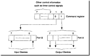
For parallel I/O, there is only one data-direction register, usually known as the "command register" for all ports. A particular bit in the command register configures all bits in the port as either inputs or outputs. Consider two I/O ports in an I/O chip along with one command register. Assume that a 0 or a 1 in a particular bit position defines all bits of ports A or B as inputs or outputs. An example is depicted in the following:

image

Some I/O ports are called "handshake ports." Data transfer occurs via these ports through exchanging of control signals between the microcomputer and an external device.

I/O ports are addressed using either standard I/O or memory-mapped I/Oclip_image004techniques. The "standard I/O" (also called "isolated I/O" by Intel) uses an output pin such as MilO pin on the Intel 8086 microprocessor chip_ The processor outputs a HIGH on this pin to indicate to memory and the I/O chips that a memory operation is taking place. A LOW output from the processor to this pin indicates an I/O operation. Execution of IN or OUT instruction makes the M/IO LOW, whereas memory-oriented instructions, such as MOVE, drive the M/IO to HIGH. In standard l/0, the processor uses the M/IO pin to distinguish between I/O and memory. For typical processors, an 8-bit address is commonly used for each I/O port. With an 8-bit 110 port address, these processors are capable of addressing 256 ports. In addition, some processors can also use 16-bit I/O ports_ However, in a typical application, four or five I/O ports may usually be required. Some of the address bits of the microprocessor are normally decoded to obtain the I/O port addresses_ With

"memory-mapped I/O", the processor, on the other hand, does not differentiate between I/O and memory, and therefore, does not use the M/10 control pin. The processor uses a portion of the memory addresses to represent I/O ports. The I/O ports are mapped as part of the processor’s main memory addresses which may not physically exist, but are used by the microprocessor’s memory-oriented instructions such as MOVE to generate the necessary control signals to perform I/O. Motorola microprocessors do not have the control pin such as M/IO pin and use only "memory-mapped 110" while Intel microprocessors can use both types.

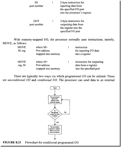
When standard I/O is used, typical processors normally use 2-byte IN or OUT instruction as follows:

image

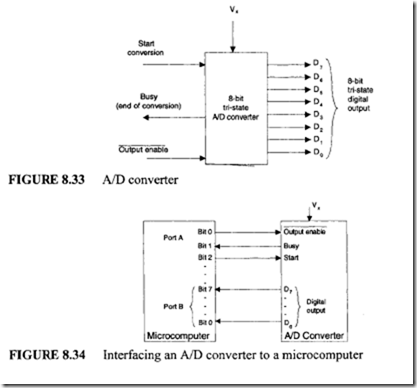
device at any time using unconditional l/0. The external device must always be ready for data transfer. A typical example is when the processor outputs a 7-bit code through an I/O port to drive a seven-segment display connected to this port. In conditional I/O, the processor outputs data to an external device via handshaking. This means that data transfer occurs via exchanging of control signals between the processor and an external device. The processor inputs the status of the external device to determine whether the device is ready for data transfer. Data transfer takes place when the device is ready. The flow chart in Figure 8.32 illustrates the concept of conditional programmed l/O.

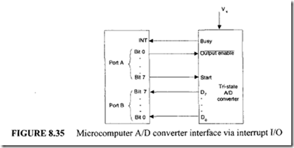
The concept of conditional l/O will now be demonstrated by means of data transfer between a processor and an analog-to-digital (A/D) converter. Consider, for example, the AID converter shown in Figure 8.33. This AID converter transforms an analog voltage Vx into an 8-bit binary output at pins D7-D0• A pulse at the START conversion pin initiates the conversion. This drives the BUSY signal LOW. The signal stays LOW during the conversion process. The BUSY signal goes to HIGH as soon as the conversion ends. Because the AID converter’s output is tristated, a LOW on the OUTPUT ENABLE transfers the converter’s outputs. A HIGH on the OUTPUT ENABLE drives the converter’s outputs to a high impedance state.

The concept of conditional I/O can be demonstrated by interfacing the AID converter to a typical processor. Figure 8.34 shows such an interfacing example. The user writes a program to carry out the conversion process. When this program is executed, the processor sends a pulse to the START pin of the converter via bit 2 of port A. The processor then checks the BUSY signal by inputting bit 1 of port A to determine if the conversion is completed. If the BUSY signal is HIGH (indicating the end of conversion), the processor sends a LOW to the OUTPUT ENABLE pin of the AID converter. The processor then inputs the converter’s D0-D7 outputs via port B. If the conversion is not completed, the

imageprocessor waits in a loop checking for the BUSY signal to go to HIGH.

8.2.2 Interrupt I/O

A disadvantage of conditional programmed I/O is that the microcomputer needs to check the status bit (BUSY signal for the AID converter) by waiting in a loop. This type of I/O transfer is dependent on the speed of the external device. For a slow device, this waiting may slow down the microcomputer’s capability of processing other data. The interrupt I/O technique is efficient in this type of situation.

Interrupt I/O is a device-initiated I/O transfer. The external device is connected

to a pin called the "interrupt (INT) pin" on the processor chip. When the device needs an I/O transfer with the microcomputer, it activates the interrupt pin of the processor chip. The microcomputer usually completes the current instruction and saves the contents of the current program counter and the status register in the stack.

The microcomputer then automatically loads an address into the program counter

to branch to a subroutine-like program called the "interrupt-service routine." This program is written by the user. The external device wants the microcomputer to execute this program to transfer data. The last instruction of the service routine is a RETURN, which is typically similar in concept to the RETURN instruction used at the end of a subroutine. The RETURN from interrupt instruction normally loads the program counter and the status register with the information saved in the stack before going to the service routine . Then, the microcomputer continues executing the main program. An example of interrupt I/O is shown in Figure 8.35.

Assume the microcomputer is MC68000 based and executing the following program:

imageThe extensions .Band.W represent byte and word operations. Note that the symbols$ and #indicate hexadecimal number and immediate mode respectively. The preceding program is arbitrarily written. The program logic can be explained using the MC68000 instruction set. Ports DDRA and DDRB are assumed to be the data-direction registers for ports A and B, respectively. The first four MOVE instructions configure bits 0 and 7 of port A as outputs and port Bas the input port, and then send a trailing START pulse (HIGH and then LOW) to the AID converter along with a HIGH to the OUTPUT ENABLE. This HIGH OUTPUT ENABLE is required to disable the AID’s output. The microcomputer continues with execution of the CLR. w DO instruction. Suppose that the BUSY signal becomes HIGH, indicating the end of conversion during execution of the CLR. W DO instruction. This drives the INT signal to HIGH, interrupting the microcomputer. The microcomputer completes execution of the current instruction, CLR. W DO. Itthen saves the current contents of the program counter (address BEGIN) and status register automatically and executes a subroutine-like program called the service routine. This program is usually written by the user. The microcomputer manufacturer normally specifies the starting address of the

service routine, or it may be provided by the user via external hardware. Assume this address is $4000, where the user writes a service routine to input the AID converter’s output as follows:

image

In this service routine, the microcomputer inputs the AID converter’s output. The return instruction RTE, at the end of the service routine, pops address BEGIN and the previous status register contents from the stack and loads the program counter and status register with them. The microcomputer executes the MOVE. W Dl, 02 instruction at address BEGIN and continues with the main program. The basic characteristics of interrupt I/O have been discussed so far. The main features of interrupt 110 provided with a typical microcomputer are discussed next.

Interrupt Types

There are typically three types of interrupts: external interrupts, traps or internal interrupts, and software interrupts. External interrupts are initiated through the microcomputer’s interrupt pins by external devices such as A/D converters. External interrupts can further be divided into two types: maskable and nonmaskable. Nonmaskable interrupt can not be enabled or disabled by instructions while microprocessor’s instruction set contains instructions to enable or disable maskable interrupt. For example, Intel 8086 can disable or enable maskable interrupt by executing instructions such as CLI (Clear interrupt flag in the Status register to 0) or STI (Set interrupt flag in the Status register to 1) . The 8086 recognizes the maskable interrupt after execution of the STI while ignores it upon execution of the CLI. Note that the 8086 has an interrupt-flag bit in the Status register. The nonmaskable interrupt has a higher priority than the maskable interrupt. If both maskable and nonmaskable interrupts are activated at the same time, the processor will service the nonmaskable interrupt first. The nonmaskable interrupt is typically used as a power failure interrupt.. Processors normally use +5 V DC, which is transformed from 110 V AC. If the power falls below 90 V AC, the DC voltage of +5 V cannot be maintained. However, it will take a few milliseconds before the AC power drops below 90 V AC. In these few milliseconds, the power-failure-sensing circuitry can interrupt the processor. The interrupt­ service routine can be written to store critical data in nonvolatile memory such as battery­ backed CMOS RAM, and the interrupted program can continue without any loss of data when the power returns.

image

Some processors such as the 8086 are provided with a maskable handshake interrupt. This interrupt is usually implemented by using two pins -INTR and INTA. When the INTR pin is activated by an external device, the processor completes the current instruction, saves at least the current program counter onto the stack, and generates an interrupt acknowledge (INTA). In response to the INTA, the external device provides an 8-bit number, using external hardware on the data bus of the microcomputer. This number is then read and used by the microcomputer to branch to the desired service routine.

Internal interrupts, or traps, are activated internally by exceptional conditions such as overflow, division by zero, or execution of an illegal op-code. Traps are handled in the same way as external interrupts. The user writes a service routine to take corrective measures and provide an indication to inform the user that an exceptional condition has occurred. Many processors include software interrupts, or system calls. When one of these instructions is executed, the processor is interrupted and serviced similarly to external or internal interrupts. Software interrupt instructions are normally used to call the operating system. These instructions are shorter than subroutine calls, and no calling program is needed to know the operating system’s address in memory. Software interrupt instructions allow the user to switch from user to supervisor mode. For some processors, a software interrupt is the only way to call the operating system, because a subroutine call to an address in the operating system is not allowed.

Interrupt Address Vector

The technique used to find the starting address of the service routine (commonly known as the interrupt address vector) varies from one processor to another. With some processors, the manufacturers define the fixed starting address for each interrupt. Other manufacturers use an indirect approach by defining fixed locations where the interrupt address vector is stored.

Saving the Microprocessor Registers

When a processor is interrupted, it saves at least the program counter on the stack so that the processor can return to the main program after executing the service routine. Typical processors save one or two registers, such as the program counter and status register, before going to the service routine. The user should know the specific registers the processor saves prior to executing the service routine. This will allow the user to use the appropriate return instruction at the end of the service routine to restore the original conditions upon return to the main program.

Interrupt Priorities

A processor is typically provided with one or more interrupt pins on the chip. Therefore, a special mechanism is necessary to handle interrupts from several devices that share one of these interrupt lines. There are two ways of servicing multiple interrupts: polled and daisy chain techniques.

i) Polled Interrupts

Polled interrupts are handled by software and are therefore are slower than daisy chaining. The processor responds to an interrupt by executing one general-service routine for all devices. The priorities of devices are determined by the order in which the routine polls each device. The processor checks the status of each device in the general-service routine, starting with the highest-priority device, to service an interrupt. Once the processor determines the source of the interrupt, it branches to the service routine for the device.

image

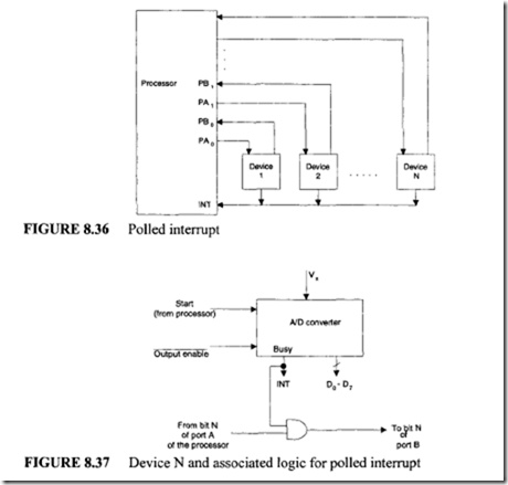
Figure 8.36 shows a typical configuration of the polled-interrupt system.

In Figure 8.36, several external devices (device 1, device 2, …, device N) are connected to a single interrupt line of the processor via an OR gate (not shown in the figure). When one or more devices activate the INT line HIGH, the processor pushes the program counter and possibly some other registers onto the stack. It then branches to an address defined by the manufacturer of the processor. The user can write a program at this address to poll each device, starting with the highest-priority device, to find the source of the interrupt. Suppose the devices in Figure 8.36 are AID converters. Each converter, along with the associated logic for polling, is shown in Figure 8.37.

Assume that in Figure 8.36 two AID converters (device 1 and device 2) are provided with the START pulse by the processor at nearly the same time. Suppose the user assigns device 2 the higher priority. The user then sets up this priority mechanism in the general-service routine. For example, when the BUSY signals from device 1 and/or 2 become HIGH, indicating the end of conversion, the processor is interrupted. In response, the processor pushes at least the program counter onto the stack and loads the PC with the interrupt address vector defined by the manufacturer.

The general interrupt-service routine written at this address determines the source of the interrupt as follows: A 1 is sent to PAl for device 2 because this device has higher priority. If this device has generated an interrupt, the output (PB 1) of the AND gate in Figure 8.37 becomes HIGH, indicating to the processor that device 2 generated the interrupt. If the output of the AND gate is 0, the processor sends a HIGH to PAO and checks the output

image

(PBO) for HIGH. Once the source of the interrupt is determined, the processor can be programmed to jump to the service routine for that device. The service routine enables the AID converter and inputs the converter’s outputs to the processor.

Polled interrupts are slow, and for a large number of devices, the time required to poll each device may exceed the time to service the device. In such a case, a faster mechanism, such as the daisy chain approach, can be used.

ii) Daisy Chain Interrupts

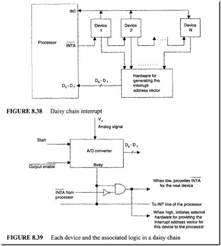
Devices are connected in a daisy chain fashion, as shown in Figure 8.38, to set up priority systems. Suppose one or more devices interrupt the processor. In response, the processor pushes at least the PC and generates an interrupt acknowledge (INTA) signal to the highest-priority device (device 1 in this case). If this device has generated the interrupt, it will accept the INTA; otherwise, it will pass the INTA onto the next device until the INTA is accepted.

Once accepted, the device provides a means for the processor to find the interrupt- address vector by using external hardware. Assume the devices in Figure 8.38 are AID converters. Figure 8.39 provides a schematic for each device and the associated logic.

Suppose the processor in Figure 8.39 sends a pulse to start the conversions of the AID converters of devices I and 2 at nearly the same time. When the BUSY signal goes to HIGH, the processor is interrupted through the INT line. The processor pushes the program counter and possibly some other registers. It then generates a LOW at the interrupt-acknowledge INTA for the highest-priority device (device 1 in Figure 8.38). Device 1 has the highest priority-it is the first device in the daisy chain configuration to receive INTA. If AID converter 1 has generated the BUSY HIGH, the output of the AND gate becomes HIGH. This signal can be used to enable external hardware to provide the interrupt-address vector on the processor’s data lines. The processor then branches to the service routine. This program enables the converter and inputs the AID output to the processor via Port B. If ND converter #1 does not generate the BUSY HIGH, however, the output of the AND gate in Figure 8.39 becomes LOW (an input to device 2’s logic) and the same sequence of operations takes place. In the daisy chain, each device has the same logic with the exception of the last device, which must accept the INTA Note that the outputs of all the devices are connected to the INT line via an OR gate (not shown in Figure 8.38)


Memory, I/O, and Parallel Processing : following example.

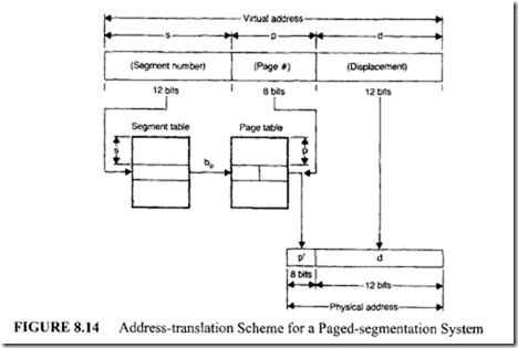
Example 8.2

Assume the following values for the system of Figure 8.14:

  • Length of the virtual address field =32 bits
  • Length of the segment number field = 12 bits
  • Length of the page number field = 8 bits
  • Length of the displacement field = 12 bits

Now, determine the value of the physical address using the following information:

  • Value of the virtual address field=000FA0BA 16
  • Contents of the segment table address (000) 16 = OFF16
  • Contents of the page table address (IF916) = AC 16

Solution

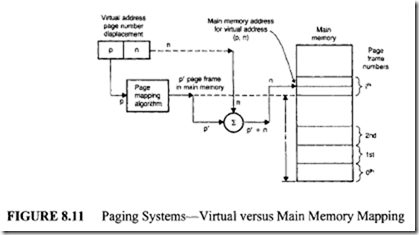
From the given virtual address, the segment table address is 00016 (three high-order hexadecimal digits of the virtual address). It is given that the contents of this segment-able address is OFF 16• Therefore, by adding the page number p (fourth and fifth hexadecimal digits of the virtual address) with OFF 16,the base address of the page table can be determined as:

0FF 16 + FA 16 = 1F916

Since the contents of the page table address 1F916 is AC 16, the physical address can be obtained by adding the displacement (low-order three hexadecimal digits of the virtual address) with AC 16 as follows:

AC000 16 + 000BA 16 = AC0BA 16

In this addition, the displacement value 0BA is sign-extended to obtain a 20-bit number that can be directly added to the base value p’. The same final answer can be obtained if p’

imageand dare first concatenated. Thus, the value of the physical address is ACOBA 16• The virtual space of some computers use both paging and segmentation, and it is called a linear segmented virtual memory system. In this system, the main memory is accessed three times to retrieve data (one for accessing the page table; one for accessing the segment table; and one for accessing the data itself).

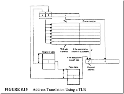
Accessing the main memory is a time-consuming operation. To speed up the retrieval operation, a small associative memory ( implemented as an on-chip hardware in modem microprocessors) called the translation lookaside buffer (TLB) is used. The TLB stores the translation information for the 8 or 16 most recent virtual addresses. The organization of a address translation scheme that includes a TLB is shown in Figure 8.15.

In this scheme, assume the TLB is capable of holding the translation information about the 8 most recent virtual addresses.

The pair (s, p) of the virtual address is known as a tag, and each entry in the TLB is of the form:

imageWhen a user program generates a virtual address, the (s, p) pair is associatively compared with all tags held in the TLB for a match. Ifthere is a match, the physical address is formed by retrieving the base address of the frame p’ from the TLB and concatenating this with the displacement d. However, in the event of a TLB miss, the physical address is generated after accessing the segment and page tables, and this information will also be loaded in the TLB. This ensures that translation information pertaining to a future reference is confined to the TLB. To illustrate the effectiveness of the TLB, the following numerical example is provided.

Example 8.3

The following measurements are obtained from a computer system that uses a linear segmented memory system with a TLB:

  • Number of entries in the TLB = 16
  • Time taken to conduct an associative search in the TLB = 160 ns
  • Main memory access time = 1 μS

Determine the average access time assuming a TLB hit ratio of 0.75.

Solution

In the event of a TLB hit, the time needed to retrieve the data is:

imageThis example shows that the use of a small TLB significantly improves the efficiency of the retrieval operation (by 33%). There are two main reasons for this improvement. First, the TLB is designed using the associated memory. Second, the TLB hit ratio may be attributed to the locality of reference. Simulation studies indicate that it is possible to achieve a hit ratio in the range of 0.8 to 0.9 by having a TLB with 8 to 16 entries.

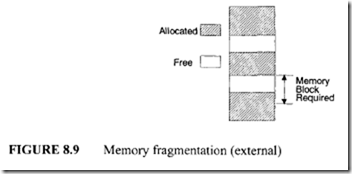
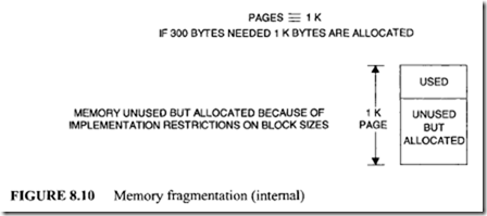
In a computer based on a linear segmented virtual memory system, the performance parameters such as storage use are significantly influenced by the page size p. For instance, when p is very large, excessive internal fragmentation will occur. If p is small, the size of the page table becomes large. This results in poor use of valuable memory space. The selection of the page size p is often a compromise. Different computer systems use different page sizes. In the following, important memory-management strategies are described. There are three major strategies associated with the management:

  • Fetch strategies
  • Placement strategies
  • Replacement strategies

All these strategies are governed by a set of policies conceived intuitively. Then they are validated using rigorous mathematical methods or by conducting a series of simulation experiments. A policy is implemented using some mechanism such as hardware, software, or firmware.

Fetch strategies deal with when to move the next page to main memory. Recall that when a page needed by a program is not in the main memory, a page fault occurs. In the event of a page fault, the page-fault handler will read the required page from the secondary memory and enter its new physical memory location in the page table, and the instruction execution continues as though nothing has happened.

In a virtual memory system, it is possible to run a program without having any page in the primary memory. In this case, when the first instruction is attempted, there is a page fault. As a consequence, the required page is brought into the main memory, where the instruction execution process is repeated again. Similarly, the next instruction may also cause a page fault. This situation is handled exactly in the same manner as described before. This strategy is referred to as demand paging because a page is brought in only when it is needed. This idea is useful in a multiprogramming environment because several programs can be kept in the main memory and executed concurrently.

However, this concept does not give best results if the page fault occurs repeatedly. For instance, after a page fault, the page- fault handler has to spend a considerable amount of time to bring the required page from the secondary memory. Typically, in a demand paging system, the effective access time tav is the sum of the main memory access time t and μ, where J1 is the time taken to service a page fault. Example 8.4 illustrates the concept.

Example 8.4

(a) Assuming that the probability of a page fault occurring is p, derive an expression for tav in terms oft, μ , and p.

(b)  Suppose that t = 500 ns and μ= 30 ms, calculate the effective access time tav if it is given that on the average, one out of 200 references results in a page fault.

Solution

(a) If a page fault does not occur, then the desired data can be accessed within a time t. (From the hypothesis the probability for a page fault not to occur is 1 –p). If the page fault occurs, then μ time units are required to access the data. The effective access time is

lav = ( 1 – P)t +

(b) Since it is given that one out of every 200 references generates a page fault, p = 1/200. Using the result derived in part (a):

lav = ((1- 0.005) X 0.5 + 0.005 X 30,000) μ S

= (0.995 X 0.5 + 150) μ S = [0.4975 + 150) μ S

= 150.4975 μ S

These parameters have a significant impact on the performance of a time-sharing system.

As an alternative approach, anticipatory fetching can be adapted. This conclusion is based on the fact that in a short period of time addresses referenced by a program are

image

clip_image005

clustered around a particular region of the address space. This property is known as locality of reference.

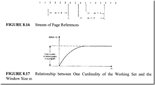
The working set of a program W(m, t) is defined as the set of m most recently needed pages by the program at some instant of time t. The parameter m is called the window of the working set. For example, consider the stream of references shown in Figure 8.16:

From this figure, determine that:

image

In general, the cardinality of the set W(O, t) is zero, and the cardinality of the set W(oo, t) is equal to the total number of distinct pages in the program. Since m + 1 most-recent page references include m most-recent page references:

#[W(m + 1, t)] #[W(m, t)]

In this equation, the symbol# is used to indicate the cardinality of the set W(m, t). When m is varied from 0 to=, #W(m, t) increases exponentially. The relationship between m and #W(m, t) is shown in Figure 8.17.

In practice, the working set of program varies slowly with respect to time. Therefore, the working set of a program can be predicted ahead of time. For example, in a multiprogramming system, when the execution of a suspended program is resumed, its present working set can be reasonably estimated based on the value of its working set at the time it was suspended. If this estimated working set is loaded, page faults are less likely to occur. This anticipatory fetching further improves the system performance because the working set of a program can be loaded while another program is being executed by the CPU. However, the accuracy of a working set model depends on the value of m. Larger values of m result in more-accurate predictions. Typical values of m lie in the range of 5000 to 10,000.

To keep track of the working set of a program, the operating system has to perform time-consuming housekeeping operations. This activity is pure overhead, and thus the system performance may be degraded.

Placement strategies are significant with segmentation systems, and they are concerned with where to place an incoming program or data in the main memory. The following are the three widely used placement strategies:

  • First-fit technique
  • Best-fit technique
  • Worst-fit technique

The first-fit technique places the program in the first available free block or hole that is adequate to store it. The best-fit technique stores the program in the smallest free hole of all the available holes able to store it. The worst-fit technique stores the program in the largest free hole. The first-fit technique is easy to implement and does not have to scan the entire space to place a program. The best-fit technique appears to be efficient because it finds an optimal hole size. However, it has the following drawbacks:
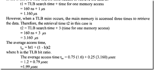
  • It is very difficult to implement.
  • It may have to scan the entire free space to find the smallest free hole that can hold the incoming program. Therefore, it may be time-consuming.
  • It has the tendency continuously to divide the holes into smaller sizes. These smaller holes may eventually become useless.

Worst-fit strategy is sometimes used when the design goal is to avoid creating small holes. In general, the operating system maintains a list known as the available space list (ASL) to indicate the free memory space. Typically, each entry in this list includes the following information:

  • Starting address of the free block
  • Size of the free block

After each allocation or release, the operating system updates the ASL. In the following example, the mechanics of the various placement strategies presented earlier are explained.

Example 8.5

The available space list of a computer memory system is specified as follows:

imageSolution

a) First-fit method. Consider the first request with a block size of25. Examination of the block sizes of the available space list reveals that this request can be satisfied by allocating from the first available block. The block size (50) is the first of the available space list and is adequate to hold the request (25 blocks). Therefore, the first request with 25 blocks will be allocated from the available space list starting at address 100 with a block size of 50. Request 1 will be allocated starting at an address of I 00 ending at an address 100 + 24 = 124 (25 locations including 100). Therefore, the first block of the available space list will start at 125 with a block size of 25. The starting address and block size of each request can be calculated similarly.

b) Best-fit method. Consider request 1. Examination of the available block size reveals that this request can be satisfied by allocating from the first smallest available block capable of holding it. Request 1 will be allocated starting at address 100 and ending at 124. Therefore, the available space list will start at 125 with a block size of25.

c) Worst-fit method. Consider request I. Examination of the available block sizes reveals that this request can be satisfied by allocating from the third block (largest) starting at 450. After this allocation the starting address of the available list will be 500 instead of 450 with a block size of600- 25 = 575. Various results for all the other requests are shown in Figure 8.18.

In a multiprogramming system, programs of different sizes may reside in the main memory. As these programs are completed, the allocated memory space becomes free. It may happen that these unused free spaces, or holes, become available between two allocated blocks, or partitions. Some of these holes may not be large enough to satisfY the memory request of a program waiting to run. Thus valuable memory space may be wasted. One way to get around this problem is to combine adjacent free holes to make the hole size larger and usable by other jobs. This technique is known as coalescing of holes.

It is possible that the memory request made by a program may be larger than

image

any free hole but smaller than the combined total of all available holes. If the free holes are combined into one single hole, the request can be satisfied. This technique is known as memory compaction. For example, the status of a computer memory before and after memory compaction is shown in Figures 8.19 and 8.20, respectively.

Placement strategies such as first-fit and best-fit are usually implemented as software procedures. These procedures are included in the operating system’s software. The advent ofhigh-levellanguages such as Pascal and C greatly simplify the programming effort because they support abstract data objects such as pointers. The available space list discussed in this section can easily be implemented using pointers.

The memory compaction task is perfonned by a special software routine of the operating system called a garbage collector. Nonnally, an operating system runs the garbage collector routine at regular intervals.

In a paged virtual memory system, when no frames are vacant, it is necessary

image

to replace a current main memory page to provide room for a newly fetched page. The page for replacement is selected using some replacement policy. An operating system implements the chosen replacement policy. In general, a replacement policy is considered efficient if it guarantees a high hit ratio. The hit ratio h is defined as the ratio of the number of page references that did not cause a page fault to the total number of page references.

The simplest of all page replacement policies is the FIFO policy. This algorithm selects the oldest page (or the page that arrived first) in the main memory for replacement. The hit ratio h for this algorithm can be analytically determined using some arbitrary stream of page references as illustrated in the following example.

Example 8.6

Consider the following stream of page requests.

2, 3, 2, 4, 6, 2, 5, 6, 1, 4, 6

Determine the hit ratio h for this stream using the FIFO replacement policy. Assume the main memory can hold 3 page frames and initially all of them are vacant.

Solution

The hit ratio computation for this situation is illustrated in Figure 8.21.

From Figure 8.21, it can be seen that the first two page references cause page faults. However, there is a hit with the third reference because the required page (page 2) is already in the main memory. After the first four references, all main memory frames are completely used. In the fifth reference, page 6 is required. Since this page is not in the main memory, a page fault occurs. Therefore, page 6 is fetched from the secondary memory. Since there are no vacant frames in the main memory, the oldest of the current main memory pages is selected for replacement. Page 6 is loaded in this position. All other data tabulated in this figure are obtained in the same manner. Since 9 out of 11 references generate a page fault, the hit ratio is 2/11.

The primary advantage of the FIFO algorithm is its simplicity. This algorithm can be implemented by using a FIFO queue. FIFO policy gives the best result when page references are made in a strictly sequential order. However, this algorithm fails if a program loop needs a variable introduced at the beginning. Another difficulty with the FIFO algorithm is it may give anomalous results.

Intuitively, one may feel that an increase in the number of page frames will also increase the hit ratio. However, with FIFO, it is possible that when the page frames are increased, there is a drop in the hit ratio. Consider the following stream of requests:

1,2,3,4,5, 1,2,5, 1,2,3,4,5,6,5

Assume the main memory has 4 page frames; then using the FIFO policy there is a hit ratio of 4/15. However, if the entire computation is repeated using 5 page frames, there

image

is a hit ratio of 3/15. This computation is left as an exercise.

Another replacement algorithm of theoretical interest is the optimal replacement policy. When there is a need to replace a page, choose that page which may not be needed again for the longest period of time in the future.

The following numerical example explains this concept.

Example 8.7

Using the optimal replacement policy, calculate the hit ratio for the stream of page references specified in Example 8.6. Assume the main memory has three frames and initially all of them are vacant.

Solution

The hit ratio computation for this problem is shown in Figure 8.22.

From Figure 8.22, it can be seen that the first two page references generate page faults. There is a hit with the sixth page reference, because the required page (page 2) is found in the main memory. Consider the fifth page reference. In this case, page 6 is required. Since this page is not in the main memory, it is fetched from the secondary memory. Now, there are no vacant page frames. This means that one of the current pages in the main memory has to be selected for replacement. Choose page 3 for replacement because this page is not used for the longest period of time. Page 6 is loaded into this position. Following the same procedure, other entries of this figure can be determined. Since 6 out of 11 page references generate a page fault, the hit ratio is 5/11.

The decision made by the optimal replacement policy is optimal because it makes a decision based on the future evolution. It has been proven that this technique does not give any anomalous results when the number of page frames is increased. However, it is not possible to implement this technique because it is impossible to predict the page references well ahead of time. Despite this disadvantage, this procedure is used as a standard to determine the efficiency of a new replacement algorithm. Since the optimal replacement policy is practically unfeasible, some method that approximates the behavior of this policy is desirable. One such approximation is the least recently used (LRU) policy.

According to the LRU policy, the page that is selected for replacement is that page that has not been referenced for the longest period of time. Example 8.8 illustrates this.

Example 8.8

Solve Example 8.7 using the LRU policy.

Solution

The hit ratio computation for this problem is shown in Figure 8.23.

In the figure we again notice that the first two references generate a page fault,

image

whereas the third reference is a hit because the required page is already in the main memory. Now, consider what happens when the fifth reference is made. This reference requires page 6, which is not in the memory.

Also, we need to replace one of the current pages in the main memory because

all frames are filled. According to the LRU policy, among pages 2, 3, and 4, page 3 is the page that is least recently referenced. Thus we replace this page with page 6. Following the same reasoning the other entries of Figure 8.23 can be determined. Note that 7 out of 11 references generate a page fault; therefore, the hit ratio is 4111. From the results of the example, we observe that the performance of the LRU policy is very close to that of the optimal replacement policy. Also, the LRU obtains a better result than the FIFO because it tries to retain the pages that are used recently.

Now, let us summarize some important features of the LRU algorithm.

  • In principle, the LRU algorithm is similar to the optimal replacement policy except that it looks backward on the time axis. Note that the optimal replacement policy works forward on the time axis.
  • If the request stream is first reversed and then the LRU policy is applied to it, the result obtained is equivalent to the one that is obtained by the direct application of the optimal replacement policy to the original request stream.
  • It has been proven that the LRU algorithm does not exhibit Belady’s anamoly. This is because the LRU algorithm is a stack algorithm. A page-replacement algorithm is said to be a stack algorithm if the following condition holds:

P1,(i) C P1(i + 1)

In the preceding relation the quantity Pt(i) refers to the set of pages in the main memory whose total capacity is i frames at some time t. This relation is called the inclusion property. One can easily demonstrate that FIFO replacement policy is not a stack algorithm. This task is left as an exercise.

  • The LRU policy can be easily implemented using a stack. Typically, the page numbers of the request stream are stored in this stack. Suppose that p is the page number being referenced. If p is not in the stack, then p is pushed into the stack. However, if p is in the stack, p is removed from the stack and placed on the top of the stack. The top of the stack always holds the most recently referenced page number, and the bottom of the stack always holds the least-recent page number. To see this clearly, consider Figure 8.24, in which a stream of page references and the corresponding stack instants are shown. The principal advantage of this approach is that there is no need to search for the page to be replaced because it is always the bottom most element of the stack. This approach can be implemented using either software or microcodes. However, this method takes more time when a page number is moved from the middle of the stack.
  • Alternatively, the LRU policy can be implemented by adding an age register to each entry of the page table and a virtual clock to the CPU. The virtual clock is organized so that it is incremented after each memory reference. When a page is referenced, its

image

age register is loaded with the contents of the virtual clock. The age register of a page holds the time at which that page was most recently referenced. The least-recent page is that page whose age register value is minimum. This approach requires an operating system to perform time-consuming housekeeping operations. Thus the performance of the system may be degraded.

  • To implement these methods, the computer system must provide adequate hardware support. Incrementing the virtual clock using software takes more time. Thus the operating speed of the entire system is reduced. The LRU policy can not be implemented in systems that do not provide enough hardware support. To get around this problem, some replacement policy is employed that will approximate the LRU policy.
  • The LRU policy can be approximated by adding an extra bit called an activity bit to each entry of the page table. Initially all activity bits are cleared to 0. When a page is referenced, its activity bit is set to I. Thus this bit tells whether or not the page is used. Any page whose activity bit is 0 may be a candidate for replacement. However, the activity bit cannot determine how many times a page has been referenced.
  • More information can be obtained by adding a register to each page table entry. To illustrate this concept, assume a 16-bit register has been added to each entry of the page table. Assume that the operating system is allowed to shift the contents of all the registers l bit to the right at regular intervals. With one right shift, the most-significant bit position becomes vacant. If it is assumed that the activity bit is used to fill this vacant position, some meaningful conclusions can be derived. For example, if the content of a page register is 0000 16,then it can be concluded that this page was not in use during the last 16 time-interval periods. Similarly, a value FFFF 16 for page register indicates that the page should have been referenced at least once in the last 16 time­ interval periods. If the content of a page register is FF00 16 and the content of another one is OOF0 16, the former was used more recently.
  • If the content of a page register is interpreted as an integer number, then the least-recent page has a minimum page register value and can be replaced. If two page registers hold the minimum value, then either of the pages can be evicted, or one of them can be chosen on a FIFO basis.
  • The larger the size of the page register, the more time is spent by the operating system in the update operations. When the size of the page register is 0, the history of the system can only be obtained via the activity bits. If the proposed replacement procedure is applied on the activity bits alone, the result is known as the second­ chance replacement policy.
  • Another bit called a dirty bit may be appended to each entry of the page table. This bit is initially cleared to 0 and set to 1 when a page is modified. This bit can be used in two different ways:
  • The idea of a dirty bit reduces the swapping overhead because when the dirty bit of a page to be replaced is zero, there is no need to copy this page into the secondary memory, and it can be overwritten by an incoming page. A dirty bit can be used in conjunction with any replacement algorithm.
  • A priority scheme can be set up for replacement using the values of the dirty and activity bits, as described next.

image 

Using the priority levels just described, the following replacement policy can be formulated: When it is necessary to replace a page, choose that page whose priority level is minimum. In the event of a tie, select the victim on a FIFO basis.

In some systems, the LRU policy is approximated using the least frequently used (LFU) and most frequently used (MFU) algorithms. A thorough discussion of these procedures is beyond the scope of this book.

  • One of the major goals in a replacement policy is to minimize the page-fault rate. A program is said to be in a thrashing state if it generates excessive numbers of page faults. Replacement policy may not have a complete control on thrashing. For example, suppose a program generates the following stream of page references:

1,2,3,4, 1,2,3,4, 1,2,3,4, …

If it runs on a system with three frames it will definitely enter into thrashing state even if the optimal replacement policy is implemented.

  • There is a close relationship between the degree of multiprogramming and thrashing. In general, the degree of multiprogramming is increased to improve the CPU use. However, in this case more thrashing occurs. Therefore, to reduce thrashing, the degree of multiprogramming is reduced. Now the CPU utilization drops. CPU utilization and thrashing are conflicting performance issues.
 

Cache Memory Organization

Cache Memory Organization

The performance of a microcomputer system can be significantly improved by introducing a small, expensive, but fast memory between the microprocessor and main memory. This memory is called "cache memory" and this idea was first introduced in the IBM 360/85 computer. Later on, this concept was also implemented in minicomputers such as the PDP-11/70. With the advent of VLSI technology, the cache memory technique is gaining acceptance in the microprocessor world. Studies have shown that typical programs spend most of their execution times in loops. This means that the addresses generated by a microprocessor have a tendency to cluster around a small region in the main memory, a phenomenon known as "locality of reference." Typical 32-bit microprocessors can execute the same instructions in a loop from the on-chip cache rather than reading them repeatedly from the external main memory. Thus, the performance is greatly improved. For example, an on-chip cache memory is implemented in Intel’s 32-bit microprocessor, the 80486/Pentium, and Motorola’s 32-bit microprocessor, the MC 68030/68040. The 80386 does not have an on-chip cache, but external cache memory can be interfaced to it.

The block diagram representation of a microprocessor system that employs a cache memory is shown in Figure 8.25. Usually, a cache memory is very small in size and

image

its access time is less than that of the main memory by a factor of 5. Typically, the access times of the cache and main memories are 100 and 500 ns, respectively_ If a reference is found in the cache, we call it a "cache hit," and the information pertaining to the microprocessor reference is transferred to the microprocessor from the cache. However, if the reference is not found in the cache, we call it a "cache miss." When there is a cache miss, the main memory is accessed by the microprocessor and, the instructions and/or data are then transferred to the microprocessor from the main memory. At the same time, a block containing the desired information needed by the microprocessor is transferred from the main memory to cache. The block normally contains 4 to 16 words, and this block is placed in the cache using the standard replacement policies such as FIFO or LRU. This block transfer is done with a hope that all future references made by the microprocessor will be confined to the fast cache.

The relationship between the cache and main memory blocks is established using mapping techniques. Three widely used mapping techniques are Direct mapping, Fully associative mapping, and Set-associative mapping. In order to explain these three mapping techniques, the memory organization of Figure 8_26 will be used. The main memory is capable of storing 4K words of 16 bits each. The cache memory, on the other hand, can store 256 words of 16 bits each. An identical copy of every word stored in cache exists in main memory. The microprocessor first accesses the cache. If there is a hit, the microprocessor accepts the 16-bit word from the cache. In case of a miss, the microprocessor reads the desired 16-bit word from the main memory and this 16-bit word is then written to the cache. A cache memory may contain instructions only (Instruction cache) or data only (Data cache) or both instructions and data (Unified cache).

Direct mapping uses a RAM for the cache. The microprocessor’s 12-bit address is divided into two fields, an index field and a tag field. Because the cache address is 8 bits wide (28 = 256), the low-order 8 bits of the microprocessor’s address form the index field, and the remaining 4 bits constitute the tag field. This is illustrated in Figure 8.26.

In general, if the main memory address field ism bits wide and the cache memory address is n bits wide, the index field will then require n bits and the tag field will be (m n) bits wide. The n-bit address will access the cache. Each word in the cache will include the data word and its associated tag. When the microprocessor generates an address for main memory, the index field is used as the address to access the cache. The tag field of

image

the main memory is compared with the tag field in the word read from cache. A hit occurs if the tags match. This means that the desired data word is in cache. A miss occurs if there is no match, and the required word is read from main memory. It is written in the cache along with the tag. One of the main drawbacks of direct mapping is that numerous misses may occur if two or more words with addresses having the same index but with different tags are accessed several times. This situation should be avoided or can be minimized by having such words far apart in the address lines. Let us now illustrate the concept of direct mapping for a data cache by means of a numerical example of Figure 8.27. All numbers are in hexadecimal.

The content of index address 00 of cache is tag= 0 and data= 013F. Suppose that the microprocessor wants to access the memory address 100. The index address 00 is used to access the cache. The memory address tag I is compared with the cache tag of 0. This does not produce a match. Therefore, the main memory is accessed and the data 2714 is transferred into the microprocessor. The cache word at index address 00 is then replaced with a tag of 1 and data of2714.

The fastest and the most expensive cache memory utilizes an associative memory. This method is known as "fully associative mapping." Each element in associative memory contains a main memory address and its content (data). When the microprocessor generates a main memory address, it is compared associatively (simultaneously) with all addresses in the associative memory. If there is a match, the corresponding data word is read from the associative cache memory and sent to the microprocessor. If a miss occurs, the main memory is accessed and the address along with its corresponding data are written to the associative cache memory. If the cache is full, certain policies such as FIFO are used as replacement algorithms for the cache. The associative cache is expensive but provides fast operation. The concept of an associative cache is illustrated by means of a numerical example in Figure 8.28. Assume all numbers are in hexadecimal.

The associative memory stores both the memory address and its contents (data).

The figure shows four words stored in the associative cache. Each word in the cache is the 12-bit address along with its 16-bit contents (data). When the microprocessor wants to access memory, the 12-bit address is placed in an address register and the associative cache memory is searched for a matching address. Suppose that the content of the microprocessor address register is 445. Because there is a match, the microprocessor reads the corresponding data OFA1 into an internal data register.

Set-associative mapping is a combination of direct and associative mapping. Each cache word stores two or more main memory words using the same index address. Each main memory word consists of a tag and its data word. An index with two or more tags and data words forms a set. When the microprocessor generates a memory request, the index of the main memory address is used as the cache address. The tag field of the main memory address is then compared associatively (simultaneously) with all tags stored under the index. If a match occurs, the desired data word is read. If a match does not occur, the

image

data word, along with its tag, is read from main memory and also written into the cache.

The hit ratio improves as the set size increases because more words with the same index but different tags can be stored in the cache. The concept of set-associative mapping can be illustrated by the numerical example shown in figure 8.29. Assume that all numbers are in hexadecimal.

Each cache word can store two or more memory words under the same index address. Each data item is stored with its tag. The size of a set is defined by the number of tag and data items in a cache word. A set size of two is used in this example. Each index address contains two data words and their associated tags.Each tag includes 4 bits, and each data word contains 16 bits. Therefore, the word length= 2 x (4 + 16) = 40 bits. An index address of 8 bits can represent 256 words. Hence, the size of the cache memory is 256 x 40. It can store 512 main memory words because each cache word includes two data words.

The hex numbers shown in Figure 8.29 are obtained from the main memory contents shown in Figure 8.27. The words stored at addresses 000 and 200 of main memory of figure 8.27 are stored in cache memory (shown in Figure 8.29) at index address 00. Similarly, the words at addresses 101 and 201 are stored at index address 01. When the microprocessor wants to access a memory word, the index value of the address is used to access the cache. The tag field of the microprocessor address is then compared with both tags in the cache associatively (simultaneously) for a cache hit. If there is a match, appropriate data is read into the microprocessor. The hit ratio will improve as the set size increases because more words with the same index but different tags can be stored in the cache. However, this may increase the cost of comparison logic.

There are two ways of writing into cache: the write-back and write-through methods. In the write-back method, whenever the microprocessor writes something into a cache word, a "dirty" bit is assigned to the cache word. When a dirty word is to be replaced with a new word, the dirty word is first copied into the main memory before it is overwritten by the incoming new word. The advantage of this method is that it avoids unnecessary writing into main memory.

In the write-through method, whenever the microprocessor alters a cache address, the same alteration is made in the main memory copy of the altered cache address. This policy can be easily implemented and also ensures that the contents of the main memory are always valid. This feature is desirable in a multiprocesssor system, in which the main memory is shared by several processors. However, this approach may lead to several unnecessary writes to main memory.

One of the important aspects of cache memory organization is to devise a method that ensures proper utilization of the cache. Usually, the tag directory contains an extra bit for each entry, called a "valid" bit. When the power is turned on, the valid bit corresponding to each cache block entry of the tag directory is reset to zero. This is done in order to indicate that the cache block holds invalid data. When a block of data is first transferred from the main memory to a cache block, the valid bit corresponding to this cache block is set to 1. In this arrangement, whenever the valid bit is zero, it implies that a new incoming block can overwrite the existing cache block. Thus, there is no need to copy the contents of the cache block being replaced into the main memory.

The performance of a system that employs a cache can be formally analyzed as follows: If tc, h, and t., specify the cache-access time, hit ratio, and the main memory access time, respectively; then the average access time can be determined as shown in the equation below:

imageThe hit ratio h always lies in the closed interval 0 and 1, and it specifies the relative number of successful references to the cache. In the above equation, when there is a cache hit, the main memory will not be accessed; and in the event of a cache miss, both main memory and cache will be accessed. Suppose the ratio of main memory access time to cache access time is y, then an expression for the efficiency of a system that employs a cache can be derived as follows:


image

This result indicates that by employing a cache, efficiency is improved by 62.5%. Assume the unit of mapping is a block; then the relationship between the main and cache memory blocks can be established by using a specific mapping technique.

In fully associative mapping, a main memory block i can be mapped to any cache blockj, where 0:%; i:%; M -1 and 0:%; j:%; N- 1 Note that the main memory has M blocks and the cache is divided into N blocks. To determine which block of main memory is stored into the cache, a tag is required for each block. Hence, Tag ( j ) = address of the main memory block stored in the cache block j.

Suppose M = 2m and N = 2n; then m and n bits are required to specify the addresses of a main and cache memory block, respectively. Also, block size = 2w, where w bits are required to specify a word in a block.

For Associative mapping : m bits of the main memory are used as a tag; and N tags are needed since there are N cache blocks.

Main memory address= (Tag+ w)bits.

For Direct mappin2: High order (m-n) bits are used as a tag.

Main memory address= (Tag+ n + w)bits

For Set-associative mappin2:

Tag field= (m- n + s) bits, where Blocks/set= 2′ Cache set number = (n – s) bits Main memory address = (Tag size + cache set number+ w ) bits.

Example 8.10

The parameters of a computer memory system are specified as follows:

  • Main memory size = 8K blocks
  • Cache memory size =512 blocks
  • Block size = 8 words

Determine the sizes of the tag field along with the main memory address using each of the following methods:

(a) Fully associative mapping

(b) Direct mapping

(c) Set associative mapping with 16 blocks/set

Solution

With the given data, compute the following:

  • M = 8K = 8192 = 2 13, and thus m = 13.
  • N = 512 = 29 , and thus n = 9.
  • Block size= 8 words= 23 words, and thus we require 3 bits to specify a word within a block.

Using this information, we can determine the main and cache memory address formats as shown next:

image

image

Examole 8.11

The access time of a cache memory is 50 ns and that of the main memory is 500 ns. It is estimated that 80% of the main memory requests are for read and the remaining are for write. The hit ratio for read access only is 0.9 and a write-through policy is used.

(a) Determine the average access time considering only the read cycles.

(b) What is the average time if the write requests are also taken into consideration

Solution

image

The growth in I C technology has allowed manufacturers to fabricate a cache on the CPU chip. The on-chip cache of Motorola’s 32-bit microprocessor, the MC68020, is discussed next.

The MC68020 on-chip cache is a direct mapped instruction cache. Only instructions are cached; data items are not. This cache is a collection of 64 entries, where each cache entry consists of a 26-bit tag field and 32-bit instruction data. The tag field

image

includes the following components:

  • High-order 24 bits of the memory address.
  • The most-significant bit FC2 of the function code. In the MC68020 processor, the 3-bit function code combination FC2 FC 1 FCO is used to identify the status of the processor and the address space (discussed in Chapter 10) of the bus cycle. For example, FC2 = 1 means the processor operates in the supervisory or privileged mode. Otherwise, it operates in the user mode. Similarly, when FC 1 FCO = 0 I, the bus cycle is made to access data. When FC 1 FCO = 10, the bus cycle is made to access code.
  • Valid bit.

A block diagram of the MC68020 on-chip cache is shown in Figure 8.30.

If an instruction fetch occurs when the cache is enabled, the cache is first checked to determine if the word requested is in the cache. This is achieved by first using 6 bits of the memory address (A7-A2) to select one of the 64 entries of the cache. Next, address bits A31-A8 and function bit FC2 are compared to the corresponding values of the selected cache entry. If there is a match and the valid bit is set, a cache hit is occurs.

In this case, the address bit AI is used to select the proper instruction word stored in the cache and the cycle ends. If there is no match or the valid bit is cleared, and a cache miss occurs. In this case, the instruction is fetched from external memory. This new instruction is automatically written into the cache and the valid bit is set. Since the processor always pre fetches instructions from the external memory in the form of long words, both instruction data words of the cache will be updated regardless of which word caused the miss.

image

The MC68020 on-chip instruction cache obtains a significant increase in performance by reducing the number of fetches required to external memory. Typically, this cache reduces the instruction execution time in two ways. First, it provides a two­ clock-cycle access time for an instruction that hits in the cache (see Figure 8.31); second, if the access hits in the cache, it allows simultaneous instruction and data access to occur. Of these two benefits, simultaneous access is more significant, since it allows 100% reduction in the time required to access the instruction rather than the 33% reduction afforded by going from three to two clocks.

Finally, microprocessors such as Intel Pentium II support two-levels of cache. These are L1 (Levell) and L2 ( Level2) cache memories. The Ll cache (Smaller in size) is contained inside the processor chip while the L2 cache ( Larger in size) is interfaced external to the microprocessor. The Ll cache normally provides separate instruction and data caches. The processor can directly access the L1 cache while the L2 cache normally supplies instructions and data to the L I cache. The L2 cache is usually accessed by the microprocessor only if L1 misses occur. This two-level cache memory enhances the performance of the microprocessor.


Virtual Memory and Memory Management concepts

8.1.3 Virtual Memory and Memory Management concepts

Due to the massive amount of information that must be saved in most systems, the mass storage device is often a disk. If each access is to a disk (even a hard disk), then system throughput will be reduced to unacceptable levels.

An obvious solution is to use a large and fast locally accessed semiconductor memory. Unfortunately the storage cost per bit for this solution is very high. A combination

image

of both off-board disk (secondary memory) and on-board semiconductor main memory must be designed into a system. This requires a mechanism to manage the two-way flow of infonnation between the primary (semiconductor) and secondary (disk) media. This mechanism must be able to transfer blocks of data efficiently, keep track of block usage, and replace them in a nonarbitrary way. The main memory system must, therefore, be able to dynamically allocate memory space.

An operating system must have resource protection from corruption or abuse by users. Users must be able to protect areas of code from each other while maintaining the ability to communicate and share other areas of code. All these requirements indicate the need for a device, located between the microprocessor and memory, to control accesses, perfonn address mappings, and act as an interface between the logical (Programmer’s memory) and the physical (Microprocessor’s directly addressable memory) address spaces. Because this device must manage the memory use configuration, it is appropriately called the "memory management unit (MMU)." Typical 32-bit processors such as the Motorola 68030/68040 and the Intel 80486/Pentium include on-chip MMUs. The MMU reduces the burden of the memory management function of the operating system.

The basic functions provided by the MMU are address translation and protection.

The MMU translates logical program addresses to physical memory address. Note that in assembly language programming, addresses are referred to by symbolic names. These addresses in a program are called logical addresses because they indicate the logical positions of instructions and data. The MMU translates these logical addresses to physical addresses provided by the memory chips. The MMU can perfonn address translation in one of two ways:

1. By using the substitution technique as shown in Figure 8.8(a)

2. By adding an offset to each logical address to obtain the corresponding physical address as shown in Figure 8.8(b) Address translation using the substitution technique is faster than the offset method. However, the offset method has the advantage of mapping a logical address to any physical address as detennined by the offset value.

Memory is usually divided into small manageable units. The tenns "page" and "segment" are frequently used to describe these units. Paging divides the memory into equal-sized pages; segmentation divides the memory into variable-sized segments. It is relatively easier to implement the address translation table if the logical and main memory spaces are divided into pages.

There are three ways to map logical addresses to physical addresses: paging,

image

FIGURE8.8

(a) Address translation using the substitution technique;

(b) Address translation by the offset technique

segmentation, and combined paging/segmentation. In a paged system, a user has access to a larger address space than physical memory provides. The virtual memory system is managed by both hardware and software. The hardware included in the memory management unit handles address translation. The memory management software in the operating system performs all functions including page replacement policies to provide efficient memory utilization. The memory management software performs functions such as removal of the desired page from main memory to accommodate a new page, transferring a new page from secondary to main memory at the right instant of time, and placing the page at the right location in memory.

If the main memory is full during transfer from secondary to main memory, it is necessary to remove a page from main memory to accommodate the new page. Two popular page replacement policies are first-in-first-out (FIFO) and least recently used (LRU). The FIFO policy removes the page from main memory that has been resident in memory for the longest amount of time. The FIFO replacement policy is easy to implement, but one of its main disadvantages is that it is likely to replace heavily used pages. Note that heavily used pages are resident in main memory for the longest amount of time. Sometimes this replacement policy might be a poor choice. For example, in a time-shared system, several users normally share a copy of the text editor in order to type and correct programs. The FIFO policy on such a system might replace a heavily used editor page to make room for a new page. This editor page might be recalled to main memory immediately. The FIFO, in this case, would be a poor choice. The LRU policy, on the other hand, replaces the page that has not been used for the longest amount of time.

In the segmentation method, the MMU utilizes the segment selector to obtain a descriptor from a table in memory containing several descriptors. A descriptor contains the physical base address for a segment, the segment’s privilege level, and some control bits. When the MMU obtains a logical address from the microprocessor, it first determines whether the segment is already in the physical memory. If it is, the MMU adds an offset component to the segment base component of the address obtained from the segment descriptor table to provide the physical address. The MMU then generates the physical address on the address bus for selecting the memory. On the other hand, if the MMU does not find the logical address in physical memory, it interrupts the microprocessor. The microprocessor executes a service routine to bring the desired program from a secondary memory such as disk to the physical memory. The MMU determines the physical address using the segment offset and descriptor as described earlier and then generates the physical address on the address bus for memory. A segment will usually consist of an integral number of pages, each, say, 256 bytes long. With different-sized segments being swapped in and out, areas of valuable primary memory can become unusable. Memory is unusable for segmentation when it is sandwiched between already allocated segments and if it is not

image

large enough to hold the latest segment that needs to be loaded. This is called "external fragmentation" and is handled by MMUs using special techniques. An example of external fragmentation is given in Figure 8.9. The advantages of segmented memory management are that few descriptors are required for large programs or data spaces and that internal fragmentation (to be discussed later) is minimized. The disadvantages include external fragmentation, the need for involved algorithms for placing data, possible restrictions on the starting address, and the need for longer data swap times to support virtual memory.

Address translation using descriptor tables offers a protection feature. A segment or a page can be protected from access by a program section of a lower privilege level. For example, the selector component of each logical address includes one or two bits indicating the privilege level of the program requesting access to a segment. Each segment descriptor also includes one or two bits providing the privilege level of that segment. When an executing program tries to access a segment, the MMU can compare the selector privilege level with the descriptor privilege level. If the segment selector has the same or higher privilege level, then the MMU permits the access. If the privilege level of the selector is lower than that of the descriptor, the MMU can interrupt the microprocessor, informing it of a privilege-level violation. Therefore, the indirect technique of generating a physical address provides a mechanism of protecting critical program sections in the operating system. Because paging divides the memory into equal-sized pages, it avoids the major problem of segmentation–external fragmentation. Because the pages are of the same size, when a new page is requested and an old one swapped out, the new one will always fit into the vacated space. However, a problem common to both techniques remains-internal fragmentation.

Internal fragmentation is a condition where memory is unused but allocated due to memory block size implementation restrictions. This occurs when a module needs, say, 300 bytes and page is lK bytes, as shown in Figure 8.10 In the paged-segmentation method, each segment contains a number of pages. The logical address is divided into three components: segment, page, and word. The segment component defines a segment number, the page component defines the page within the segment, and the word component provides the particular word within the page. A page component of n bits can provide up to 2" pages. A segment can be assigned with one or more pages up to maximum of 2" pages; therefore, a segment size depends on the number of pages assigned to it.

A protection mechanism can be assigned to either a physical address or a logical address. Physical memory protection can be accomplished by using one or more protection bits with each block to define the access type permitted on the block. This means that

image

each time a page is transferred from one block to another, the block protection bits must be updated. A more efficient approach is to provide a protection feature in logical address space by including protection bits in descriptors of the segment table in the MMU.

Virtual memory is the most fundamental concept implemented by a system that performs

memory-management functions such as space allocation, program relocation, code sharing and protection. The key idea behind this concept is to allow a user program to address more locations than those available in a physical memory. An address generated by a user program is called a virtual address. The set of virtual addresses constitutes the virtual address space. Similarly, the main memory of a computer contains a fixed number of addressable locations and a set of these locations forms the physical address space. The basic hardware for virtual memory is implemented in modern microprocessors as an on­ chip feature. These contemporary processors support both cache and virtual memories. The virtual addresses are typically converted to physical addresses and then applied to cache.

In the early days, when a programmer used to write a large program that could not fit into the main memory, it was necessary to divide the program into small portions so each one could fit into the primary memory. These small portions are called overlays. A programmer has to design overlays so that they are independent of each other. Under these circumstances, one can successively bring each overlay into the main memory and execute them in a sequence.

Although this idea appears to be simple, it increases the program-development time considerably.

However, in a system that uses a virtual memory, the size of the virtual address space is usually much larger than the available physical address space. In such a system, a programmer does not have to worry about overlay design, and thus a program can be written assuming a huge address space is available. In a virtual memory system, the programming effort can be greatly simplified. However, in reality, the actual number of physical addresses available is considerably less than the number of virtual addresses provided by the system. There should be some mechanism for dividing a large program into small overlays automatically. A virtual memory system is one that mechanizes the process of overlay generation by performing a series of mapping operations.

A virtual memory system may be configured in one of the following ways:

  • Paging systems
  • Segmentation systems

In a paging system, the virtual address space is divided into equal-size blocks called pages. Similarly, the physical memory is also divided into equal-size blocks called frames. The size of a page is the same as the size of a frame. The size of a page may be 512, 1024 or 2048 words.

In a paging system, each virtual address may be regarded as an ordered pair (p, n), where pis the page number and n is the word number within the page p. Sometimes the quantity n is referred to as the displacement, or offset. A user program may be regarded as a sequence of pages, and a complete copy of the program is always held in a backup store such as a disk. A page p of the user program can be placed in any available page frame p’ of the main memory. A program may access a page if the page is in the main memory. In a paging scheme, pages are brought from secondary memory and are stored in main memory in a dynamic manner. All virtual addresses generated by a user program must be translated into physical memory addresses. This process is known as dynamic address translation and is shown in Figure 8.11.

When a running program accesses a virtual memory location v = (p, n), the

image

mapping algorithm finds that the virtual page p is mapped to the physical frame p’. The physical address is then determined by appending p’ ton.

This dynamic address translator can be implemented using a page table. In most systems, this table is maintained in the main memory.lt wiii have one entry for each virtual page of the virtual address space. This is illustrated in the following example.

Example 8.1

Design a mapping scheme with the following specifications:

  • Virtual address space= 32K words
  • Main memory size = 8K words
  • Page size = 2K words
  • Secondary memory address = 24 bits

Solution

32K words can be divided into 16 virtual pages with 2K words per page, as

follows:·


image


image

Since there are 32K addresses in the virtual space, 15 bits are required for the virtual address. Because there are 16 virtual pages, the page map table contains 16 entries. The 4 most-significant bits of the virtual address are used as an index to the page map table, and the remaining 11 bits of the virtual address are used as the displacement to locate a word within the page frame. Each entry of the page table is 32 bits long. This can be obtained as follows:

1 bit for determining whether the page table is in main memory or not (residence bit).

2 bits for main memory page frame number.

24 bits for secondary memory address

5  bits for future use. (Unused)

32 bits total

The complete layout of the page table is shown in Figure 8.12. Assume the virtual address generated is 0111 000 0010 1101. From this, compute the following:

Virtual page number = 710

Displacement = 43 10

From the page-map table entry corresponding to the address 0Ill, the page can be found in the main memory (since the page resident bit is 1).

The required virtual page is mapped to main memory page frame number 2. Therefore, the actual physical word is the 43rd word in the second page frame of the main memory.

So far, a page referenced by a program is assumed always to be found in the main memory. In practice, this is not necessarily true. When a page needed by a program is not assigned to the main memory, a page fault occurrs. A page fault is indicated by an interrupt, and when this interrupt occurs, control is transferred to a service routine of the operating system called the page-fault handler. The sequence of activities performed by the page­ fault handler are summarized as follows:

  • The secondary memory address of the required page pis located from the page table.
  • Page p from the secondary memory is transferred into one of the available main memory frames by performing a block-move operation.
  • The page table is updated by entering the frame number where page p is loaded and by setting the residence bit to 1 and the change bit to 0.

When a page-fault handler completes its task, control is transferred to the user program, and the main memory is accessed again for the required data or instruction. All

image

these activities are kept hidden from a user. Pages are transferred to main memory only at specified times. The policy that governs this decision is known as the fetch policy. Similarly, when a page is to be transferred from the secondary memory to main memory, all frames may be full. In such a situation, one of the frames has to be removed from the main memory to provide room for an incoming page. The frame to be removed is selected using a replacement policy. The performance of a virtual memory system is dependent upon the fetch and replacement strategies. These issues are discussed later.

The paging concept covered so far is viewed as a one-dimensional technique because the virtual addresses generated by a program may linearly increase from 0 to some maximum value M. There are many situations where it is desirable to have a multidimensional virtual address space. This is the key idea behind segmentation systems.

Each logical entity such as a stack, an array, or a subroutine has a separate virtual address space in segmentation systems. Each virtual address space is called a segment, and each segment can grow from zero to some maximum value. Since each segment refers to a separate virtual address space, it can grow or shrink independently without affecting other segments.

In a segmentation system, the details about segments are held in a table called a segment table. Each entry in the segment table is called a segment descriptor, and it typically includes the following information:

  • Segment base address b (starting address of the segment in the main memory)
  • Segment length l (size of a segment)

image

  • Segment presence bit
  • Protection bits

From the structure of a segment descriptor, it is possible to create two or more segments whose sizes are different from one another. In a sense, a segmentation system becomes a paging system if all segments are of equal length. Because of this similarity, there is a close relationship between the paging and segmentation systems from the viewpoint of address translation.

A virtual address, V, in a segmentation system is regarded as an ordered pair (s, d), where s is the segment number and d is the displacement within segments. The address translator for a segmentation system can be implemented using a segment table, and its organization is shown in Figure 8.13.

The details of the address translation process is briefly discussed next.

Let V be the virtual address generated by the user program. First, the segment number field, s, of the virtual address Vis used as an index to the segment table. The base address and length of this segment are b, and!,, respectively. Then, the displacement d of the virtual address V is compared with the length of the segment l, to make sure that the required address lies within the segment. If d is less than or equal to !,then the comparator output Z will be high. When d s !, ,the physical address is formed by adding b, and d. From this physical address, data is retrieved and transferred to the CPU. However, when d > !,
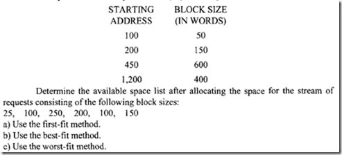
, the required address lies out of the segment range, and thus an address out of range trap will be generated. A trap is a nonmaskable interrupt with highest priority.

In a segmentation system, a segment needed by a program may not reside in main memory. This situation is indicated by a bit called a valid bit. A valid bit serves the same purpose as that of a page resident bit, and thus it is regarded as a component of the segment descriptor. When the valid bit is reset to 0, it may be concluded that the required segment is not in main memory.

This means that its secondary memory address must be included in the segment descriptor. Recall that each segment represents a logical entity. This implies that we can protect segments with different protection protocols based on the logical contents of the segment. The following are the common protection protocols used in a segmentation system:

  • Read only
  • Execute only
  • Read and execute only
  • Unlimited access
  • No access

Thus it follows that these protection protocols have to be encoded into some protection codes and these codes have to be included in a segment descriptor.

In a segmented memory system, when a virtual address is translated into a physical address, one of the following traps may be generated:

  • Segment fault trap is generated when the required segment is not in the main memory.
  • Address violation trap occurs when d >/,.
  • Protection violation trap is generated when there is a protection violation.

When a segment fault occurs, control will be transferred to the operating system. In response, the operating system has to perform the following activities:

  • First, it finds the secondary memory address of the required segment from its segment descriptor.
  • Next, it transfers the required segment from the secondary to primary memory. Finally, it updates the segment descriptor to indicate that the required segment is in the main memory.

After performing the preceding activities, the operating system transfers control to the user program and the data or instruction retrieval or write operation is repeated.

A comparison of the paging and segmentation systems is provided next. The primary idea behind a paging system is to provide a huge virtual space to a programmer, allowing a programmer to be relieved from performing tedious memory-management tasks such as overlay design. The main goal of a segmentation system is to provide several virtual address spaces, so the programmer can efficiently manage different logical entities such as a program, data, or a stack.

The operation of a paging system can be kept hidden at the user level. However,a programmer is aware of the existence of a segmented memory system.

To run a program in a paging system, only its current page is needed in the main memory. Several programs can be held in the main memory and can be multiplexed. The paging concept improves the performance of a multiprogramming system. In contrast, a segmented memory system can be operated only if the entire program segment is held in the main memory.

In a paging system, a programmer cannot efficiently handle typical data structures

such as stacks or symbol tables because their sizes vary in a dynamic fashion during program execution. Typically, large pages for a symbol table or small pages for a stack cannot be created. In a segmentation system, a programmer can treat these two structures as two logical entities and define the two segments with different sizes.

The concept of segmentation encourages people to share programs efficiently. For example, assume a copy of a matrix multiplication subroutine is held in the main memory. Two or more users can use this routine if their segment tables contain copies of

the segment descriptor corresponding to this routine. In a paging system, this task cannot be accomplished efficiently because the system operation is hidden from the user. This result also implies that in a segmentation system, the user can apply protection features to each segment in any desired manner. However, a paging system does not provide such a versatile protection feature.

Since page size is a fixed parameter in a paging system, a new page can always be

loaded in the space used by a page being swapped out. However, in a segmentation system with uneven segment sizes, there is no guarantee that an incoming segment can fit into the free space created by a segment being swapped out.

In a dynamic situation, several programs may request more space, whereas some

other programs may be in the process of releasing the spaces used by them. When this happens in a segmented memory system, there is a possibility that uneven-sized free spaces may be sparsely distributed in the physical address space. These free spaces are so irregular in size that they cannot normally be used to satisfy any new request. This is called an external fragmentation, and an operating system has to merge all free spaces to form a single large useful segment by moving all active segments to one end of the memory. This activity is known as memory compaction. This is a time-consuming operation and is a pure overhead. Since pages are of equal size, no external fragmentation can occur in a paging system.

In a segmented memory system, a programmer defines a segment, and all segments are completely filled.

The page size is decided by the operating system, and the last page of a program may not be filled completely when a program is stored in a sequence of pages. The space not filled in the last page cannot be used for any other program. This difficulty is known as internal fragmentation-a potential disadvantage of a paging system.
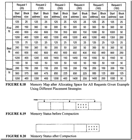
In summary, the paging concept simplifies the memory-management tasks to be performed by an operating system and therefore, can be handled efficiently by an operating system. The segmentation approach is desirable to programmers when both protection and

image

sharing of logical entities among a group of programmers are required.

To take advantage of both paging and segmentation, some systems use a different approach, in which these concepts are merged. In this technique, a segment is viewed as a collection of pages. The number of pages per segment may vary. However, the number of words per page still remains fixed. In this situation, a virtual address V is an ordered triple (s, p, d), where s is the segment number and p and dare the page number and the displacement within a page, respectively.

The following tables are used to translate a virtual address into a physical address:

Page table: This table holds pointers to the physical frames.

Segment table: Each entry in the segment table contains the base address of the page table that holds the details about the pages that belong to the given segment.

The address-translation scheme of such a paged-segmentation system is shown in Figure 8.14:

  • First, the segment number s of the virtual address is used as an index to the segment table, which leads to the base address bP of the page table.
  • Then, the page number p of the virtual address is used as an index to the page table, and the base address of the frame number p’ (to which the page p is mapped) can be found.
  • Finally, the physical memory address is computed by adding the displacement d of the virtual address to the base address p’ obtained before.

To illustrate this concept, the following numerical example is provided.


Memory, I/O, and parallel processing : memory organization , introduction and main memory array design

8.1 Memory Organization

8.1.1 Introduction

A memory unit is an integral part of any microcomputer system, and its primary purpose is to hold instructions and data. The major design goal of a memory unit is to allow it to operate at a speed close to that of the processor. However, the cost of a memory unit is so prohibitive that it is practically not feasible to design a large memory unit with one technology that guarantees a high speed. Therefore, in order to seek a trade-off between the cost and operating speed, a memory system is usually designed with different technologies such as solid state, magnetic, and optical.

In a broad sense, a microcomputer memory system can be divided into three

groups:

  • Processor memory
  • Primary or main memory
  • Secondary memory

Processor memory refers to a set of microprocessor registers. These registers are used to hold temporary results when a computation is in progress. Also, there is no speed disparity between these registers and the microprocessor because they are fabricated using the same technology. However, the cost involved in this approach limits a microcomputer architect to include only a few registers in the microprocessor. The design of typical registers is described in Chapters 5, 6 and 7.

Main memory is the storage area in which all programs are executed. The microprocessor can directly access only those items that are stored in main memory. Therefore, all programs must be within the main memory prior to execution. CMOS technology is normally used these days in main memory design. The size of the main memory is usually much larger than processor memory and its operating speed is slower than the processor registers. Main memory normally includes ROMs and RAMs. These are described in Chapter 6.

Electromechanical memory devices such as disks are extensively used as microcomputer’s secondary memory and allow storage of large programs at a low cost. These secondary memory devices access stored data serially. Hence, they are significantly slower than the main memory. Popular secondary memories include hard disk and floppy disk systems. Programs are stored on the disks in files. Note that the floppy disk is removable whereas the hard disk is not. Secondary memory stores programs in excess of the main memory. Secondary memory is also referred to as "auxiliary" or "virtual" memory. The microcomputer cannot directly execute programs stored in the secondary memory, so in order to execute these programs, the microcomputer must transfer them to its main memory by a program called the "operating system."

Programs in disk memories are stored in tracks. A track is a concentric ring of programs stored on the surface of a disk. Each track is further subdivided into several sectors. Each sector typically stores 512 or 1024 bytes of information. All secondary memories use magnetic media except the optical memory, which stores programs on a plastic disk. CD-ROM is an example of a popular optical memory used with microcomputer systems. The CD-ROM is used to store large programs such as a C++ compiler. Other state-of-the-art optical memories include CD-RAM, DVD-ROM and DVD-RAM. These optical memories are discussed in Chapter 1.

In the past, one of the most commonly used disk memory with microcomputer systems was the floppy disk. The floppy disk is a flat, round piece of plastic coated with magnetically sensitive oxide material. The floppy disk is provided with a protective jacket to prevent fingerprint or foreign matter from contaminating the disk’s surface. The 3Y2- inch floppy disk was very popular because of its smaller size and because it didn’t bend easily. All floppy disks are provided with an off-center index hole that allows the electronic system reading the disk to find the start of a track and the first sector.

The storage capacity of a hard disk varied from 10 megabytes (MB) in 1981 to hundreds of gigabytes (GB) these days. The 3 Y:z-inch floppy disk, on the other hand, can typically store 1.44 MB. Zip disks were an enhancement in removable disk technology providing storage capacity of I 00 MB to 750 MB in a single disk with access speed similar to the hard disk. Zip disk does not use a laser. Rather, it uses a magnetic-coated Myler inside, along with smaller read/write heads, and a rotational speed of 3000 rpm. The smaller heads allow the Zip drive to store programs using 2, 118 tracks per inch, compared to 135 tracks per inch on a floppy disk. Floppy disks are being replaced these days by USB (Universal Serial Bus) Flash memory. Note that USB is a standard connection for computer peripherals such as CD burners. Also, flash memory gets its name because the technology uses microchips that allow a section of memory cells called blocks to be erased in a single action called a "flash". USB flash memory offers much more storage capacity than floppy disks, and can typically store I 6 megabytes up to multiple gigabytes of information.

8.1.2 Main Memory Array Design

From the previous discussions, we notice that the main memory of a microcomputer is fabricated using solid-state technology. In a typical microcomputer application, a designer has to implement the required capacity by interconnecting several small memory chips. This concept is known as the "memory array design." In this section, we address this topic. We also show how to interface a memory system with a typical microprocessor.

Now let us discuss how to design ROM/RAM arrays. In particular, our discussion is focused on the design of memory arrays for a hypothetical microcomputer. The pertinent signals of a typical microprocessor necessary for main memory interfacing are shown in

imageFigure 8.1. In Figure 8.1, there are 16 address lines, A 15 through ‘ with A0 being the least significant bit. This means that this microprocessor can directly address a maximum of 2 16

= 65,536 or 64K bytes of memory locations. The control line M/IO goes to LOW if the microprocessor executes an I/0 instruction, and it is held HIGH if the processor executes a memory instruction. Similarly, the control line R/W goes to HIGH to indicate that the operation is READ and it goes to LOW for WRITE operation. Note that all 16 address lines and the two control lines described so far are unidirectional in nature; that is, information can always travel on these lines from the processor to external units. Also, in Figure 8.1 eight bidirectional data lines D7 through D0 (with D0 being the least significant bit) are shown. These lines are used to allow data transfer from the processor to external units and vice versa.

In a typical application, the total amount of main memory connected to a microprocessor consists of a combination of both ROMs and RAMs. However, in the following we will illustrate for simplicity how to design memory array using only the RAM chips.

The pin diagram of a typical lK x 8 RAM chip is shown in Figure 8.2. In this RAM chip there are 10 address lines, A9 through A0, so one can read or write 1024 (210 = 1024) different memory words. Also, in this chip there are 8 bidirectional data lines D7 through D0 so that information can travel back and forth between the microprocessor and the memory unit. The three control lines CS 1, CS2, and RIW are used to control the RAM unit according to the truth table shown in Figure 8.3. From this truth table it can be concluded that the RAM unit is enabled only when CS 1 = 0 and CS2 = 1. Under this condition, RIW = 0 and R!W = 1 imply write and read operations respectively.

To connect a microprocessor to ROM/RAM chips, three address-decoding techniques are usually used: linear decoding, full decoding, and memory decoding using

image

PLD. Let us first discuss how to interconnect a microprocessor with a 4K RAM chip array comprised of the four 1K RAM chips of Figure 8.2 using the linear decoding technique. Figure 8.4 uses the linear decoding to accomplish this.

In this approach, the address lines A9 through A0 of the microprocessor are connected to all RAM chips. Similarly, the control lines M/IO and RIW of the microprocessor are connected to the control lines CS2 and RIW respectively of each RAM chip. The high­ order address bits A 10 through A 13 directly act as chip selects.

In particular, the address lines A 10 and A 11 select the RAM chips I and II respectively. Similarly, the address lines A 12 and A 13 select the RAM chips III and IV respectively. A 15 and A 14 are don’t cares and are assumed to be 0. Figure 8.5 describes how

image

image

the addresses are distributed among the four 1K RAM chips. This method is known as "linear select decoding," and its primary advantage is that it does not require any decoding hardware. However, if two or more lines of A 10 through A 13 are low at the same time, more than one RAM chip are selected, and this causes a bus conflict. Because of this potential problem, the software must be written in such a way that it never reads into or writes from any address in which more than one of the bits A 13 through A 10 are low. Another disadvantage of this method is that it wastes a large amount of address space. For example,

image

whenever the address value is 8800 or 3800, the RAM chip I is selected. In other words, the address 3800 is the mirror reflection of the address 8800 (this situation is also called "memory foldback"). This technique is, therefore, limited to a small system. In particular, we can extend the system of Figure 8.4 up to a total capacity of 6K using A 14 and A 15 as chip selects for two more 1K RAM chips.

To resolve the problems with linear decoding, we use the full decoded memory

addressing. In this technique, we use a decoder. The same 4K memory system designed using this technique is shown in Figure 8.6. Note that the decoder in the figure is very similar to a practical decoder such as the 74LS138 with three chip enables. In Figure 8.6 the decoder output selects one of the four IK RAM chips depending on the values of A 12, A 11,and A 10• Note that the decoder output will be enabled only when E3 = E2 = 0 and El = I. Therefore, in the organization of Figure 8.6, when any one of the high-order bits A 15,A 14,

or A 13 is 1, the decoder will be disabled, and thus none of the RAM chips will be selected. In this arrangement, the memory addresses are assigned as shown in Figure 8.7.

This approach does not waste any address space since the unused decoder outputs (don’t cares) can be used for memory expansion. For example, the 3-to-8 decoder of Figure 8.6 can select eight lK RAM chips. Also, this method does not generate any bus conflict. This is because the selected decoder output ensures enabling of one memory chip at a time.

As mentioned before, a Programmable Logic Device (PLD) is similar to a ROM in concept except that it does not provide full decoding of the input lines. Instead, a PLD provides a partial sum of products that can be obtained via programming and saves a lot of space on the board. For example, a PAL chip contains a fused programmable AND array and a fixed OR array. Note that both AND and OR arrays are programmable in a PLA. The AND and OR gates are fabricated inside the PLD without interconnections. The specific functions desired are implemented during programming via software. For example, programming of the PAL provides connections of the AND gates to the inputs of the OR gates. Therefore, the PAL implements the sum of the products of the inputs. PLDs are used extensively these days with 32- and 64-bit microprocessors such as the Intel 80386/80486/Pentium and Motorola 68030/68040/PowerPC for performing the memory decode function. PLDs connect these microprocessors to memory, 1/0 devices, and other chips without the use of any additional logic gates or circuits.


QUESTIONS AND PROBLEMS

QUESTIONS AND PROBLEMS

7.1 It is desired to implement the following instructions using block code: ADD, SUB, XOR, MOVE, HALT. Draw a block diagram.

7.2 The instruction length and the size of an address field are 9 bits and 3 bits respectively. Is it possible to have

6 two-address instructions

15 one-address instructions

8 zero-address instructions

using expanding op-code technique? Justify your answer.

7.3 Using the instruction format of Problem 7.2, is it possible to have

7 two-address instructions

7 one-address instructions

8 zero-address instructions

using expanding opcode technique? Justify your answer.

7.4 Assume that it is desired to have 2 two-address, 7 one-address, and 25 zero­ address instructions in a computer instruction set. Using expanding op-code technique with a 2-bit op-code and 3-bit address field, is it possible to accomplish the above? If so, justify your answer and determine the instruction length.

7.5 Assume that using an instruction length of 9 bits and the address field size of 3 bits, 5 two-address and 10 one-address instructions have already been designed, using expanding op-code technique. Is it possible to have at least 48 zero-address instructions that can be added to the instruction set?

7.6 Design a combinational logic shifter with 4-bit input and 4-bit output as follows:

image7.7 Draw a logic diagram for a 4 x 4 barrel shifter.

7.8 Using a minimum number of full adders and multiplexers, design an incrementer/ decrementer circuit as follows: If S = 0, output y = x + I; otherwise, y = x – I. Assume x andy are 4-bit signed numbers and the result is 4 bits wide.

7.9 Design a combinational circuit to compute the absolute value of an 8-bit twos complement number. Use 8-bit binary adder and exclusive-OR gates. Draw a logic circuit.

7.10 Using a 4-bit CLA as the building block, design an 8-bit adder.

7.11  Design:

 (a)   a 16-bit adder whose worst-case add-time is 1Oil using a 4-bit CLA as a building block.

(b) the fastest 64-bit adder using a 4-bit CLA as the building block. Estimate the worst-case add-time of your design.

(c)   a combinational circuit to compute the functionf(x) = (3/8) * x where x is a 4-bit 2’s complement number.

7.12 Design an arithmetic logic unit to perform the following functions:

imageUse multiplexers, binary adders, and gates as needed. Assume that A and B are 4-bit numbers. Draw a logic circuit.

7.13 Design a combinational circuit that will perform the following operations:

imageAssume that A is a 4-bit number and B =image Draw a logic diagram.

7.14 Design a 4-bit ALU to perform the following operations:

image

Assume that A is a 4-bit number. Draw a logic diagram using a binary adder, multiplexers, and inverters as necessary.

7.15 Design a 4-bit arithmetic unit as follows:

image

Assume that A and B are 4-bit numbers .

7.16 Design an ALU to perform the following operations:

imageAssume that x andy are 4-bit numbers, and B= image. Draw a logic diagram.

7.17 Assume two 2’s complement signed numbers, M= 111111112 and Q= 111111002

Perform the signed multiplication using the algorithm described in Section 7.2.2.

7.18 What is the purpose of the control unit in a microprocessor?

7.19 Draw a logic diagram to implement the following register transfers:

(a) If the content of the 8-bit register R is odd, then

image(b) If the number in the 8-bit register R is negative, then x x- 1 else x <— x + 1. Assume x andy are 4 bits wide.

7.20 Discuss briefly the merits and demerits of single-bus, two-bus, and three-bus architectures inside a control unit.

7.21 What is the basic difference between hardwired control, microprogramming, and nanoprogramming? Name the technique used for designing the control units of the Intel 8086, Motorola 68000, and PowerPC.

7.22 Using the following components: 4-bit general-purpose register, 4-bit adder/subtractor, and tristate buffer, and assuming the inbus and outbus are

4 bits wide, design a control unit using hardwired control to perform the following operations. You may use counters, decoders, and PLAs as required.

image7.23 Repeat Problem 7.22 using microprogramming.

7.24 Discuss the basic differences between microprogramming and nano­ programming.

7.25 (a) A conventional microprogrammed control unit includes 1024 words by 85 bits. Each of 512 microinstructions are unique. Calculate the savings if any by having a nanomemory. Calculate the sizes of microcontrol memory and nanomemory.

(b) Consider the following 14 x 6 microprogram using a conventional control memory:

image

Implement this microprogram in a nanomemory. Justify the use of either a single­ control memory or a two-level memory for the program.
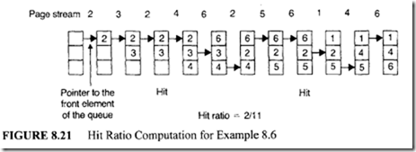
7.26 Discuss the basic differences between CISC and RISC.

7.27 Design and implement a combinational circuit that will work as follows:

image

7.28          i) Design a combinational circuit that will satisfy the following specification.

image

image

7.29 Design a 4-bit, 8-function arithmetic unit that will meet the following specifications:

image

7.31 Design and implement a 6 x 6 array multiplier.

7.32 Design an unsigned 8 x 4 non-additive multiplier using additive-multiplier­ module whose block diagram representation is as follows:

image

Assume that M, Q, and Y are unsigned integers.

7.33 Using four 256 x 8 ROMS and 4-bit parallel adders, design a 8 x 8 unsigned, nonadditive multiplier. Draw a logic diagram of your implementation.

7.34 Consider the registers and ALU shown in Figure P7.34:

image

(a) How will the A register be cleared? (Suggest at least two possible ways.) DIRECT CLEAR input is not available.

(b) Suggest a sequence of control words that exchanges the contents of A and B registers (exchange means A Band B A).

7.35 Consider the following algorithm:

image

Design a hardwired controller that will implement this algorithm.

7.36 It is desired to build an interface in order establish communication between a 32- bit host computer and a front end 8-bit microcomputer (See Figure P7.36). The operation of this system is described as follows:

Step 1: First the host processor puts a high signal on the line "want" (saying that it needs a 32-bit data) for one clock period.

Step 2: The interface recognizes this by polling the want line.

Step 3: The interface unit puts a high signal on the line "fetch" for one clock period (that is it instructs the microcomputer to fetch an 8-bit data).

Step 4: In response to this, the microcomputer samples the speech signal, converts it into an 8-bit digital data and informs the interface that the data is ready by placing a high signal on the "ready" line for one clock period.

Step 5: The interface recognizes this (by polling the ready line), and it reads the 8-bit data into its internal register.

Step 6: The interface unit repeats the steps 3 through 5 for three more times (so that it acquires 32-bit data from the microcomputer).

Step 7: The interface informs the host computer that the latter can read the 32-bit data by placing a high signal on the line "takeit" for one clock period.

Step 8: The interface unit maintains a valid 32-bit data on the 32-bit output bus until the host processor says that it is done (the host puts a high signal on the line "done" for one clock period). In this case, the interface proceeds to step 1 and looks for a high on the "want" line.

(a) Provide a Register Transfer Language description of the interface.

(b) Design the processing section of the interface.

{c) Draw a block diagram ofthe interface controller.

(d) Draw a state diagram of the interface controller.

image

7.37 Solve Problem 7.35 using the microprogrammed approach.

7.38 Design a microprogrammed system to add numbers stored in the register pair AB and CD. A, B, C, and D are 8-bit registers. The sum is to be saved in the register pair AB. Assume that only an 8-bit adder is available.

7.39 The goal of this problem is to design a microprogrammed 3rd order FIR (Finite impulse response) digital filter. In this system, there are 4 coefficients w0, w 1 , w2, and w3• The output Yk (at the kth clock period) is the discrete convolution product of the inputs (x ) and the filter coefficients. This is formally expressed as follows:

imageIn the above summation, xk represents the input at the kth clock period

whilexk-i represents input at (k- i)th sample period. For all practical purposes, we assume that our system is causal and so xi= 0 for i < 0. The processing hardware is shown in Figure P7.39. This unit includes 8 eight-bit registers (to hold data and coefficients), AID (Analog digital converter), MAC (multiplier accumulator), and a D/A (Digital analog converter). The processing sequence is shown below:

1 Initialize coefficient registers

2 Clear all data registers except xi

3 Start AID conversion (first make sc = I and then retract it to 0)

4 Wait for one control state (To make sure that the conversion is complete)

5 Read the digitized data into the register xk

6 Iteratively calculate filter output Yk (use MAC for this)

7 Pass Yk to D/A (Pass Accumulator’s output to DIA via Rounding ROM)

8 Move the data to reflect the time shift (x k- 3 = x k _ 2 , x k _ 2 = x k _ 1 , x k- 1 =x k)

9 Go to 3

(a) Specify the controller organization.

(b) Produce a well documented listing of the binary microprogram

image7.40 Your task is to design a microprogrammed controller for a simple robot with 4 sensors (see Fig. A). The sensor output will go high only if there is a wall or an obstruction within a certain distance. For example, ifF= 1, there is an obstruction or wall in the forward direction. In particular, your controller is supposed to communicate with a motor controller unit shown in Fig. B. The flow chart that describes the control algorithm is shown in Fig. C. The outputs such as MFTS, MRT, MLT, MUT, and STP, andd the status signals such as FMC, and TC will be high for one clock period. Assume that a power on reset causes the controller to go the WAIT STATE 0.

image

image

7.41 It is desired to add the following instructions to the instruction set shown in Figure 7.54.

image

7.42 Explain how the effect of an unconditional branch instruction of the following form is simulated:

JP <addr>

Use the instruction set shown in Figure 7.54.

7.43 Using the instruction set shown in Figure 7.54, write a program to add the contents of the memory locations 6416 through 6D 16 and save the result in the address 6E 16•

7.44 Show that it is possible to specify 675 microoperations using a 10 bit control function field.

7.45 A microprogram occupies 100 words and each word typically emits 70 control signals. The architect claims that by using a 2i x 70 nanomemory (for some i > 0), it is possible to save 4260 bits. If this were true, determine the number of distinct control states in the original microprogram (Note that here when we say a control state we refer only to the control function field).

Hint: You may have to employ a trial and error approach to solve this problem.


Design of a Microprogrammed CPU

7.4 Design of a Microprogrammed CPU

Next, the design of a microprogrammed processor is illustrated. The programming model of this processor is shown in Figure 7.52.

The CPU contains two registers:

1. An 8-bit register A                               2. A 2-bit flag register F

The flag register holds only zero (Z) and carry (C) flags. All programs and data are stored in the 256 x 8 RAM. The detailed hardware schematic of the data-flow part of this processor is shown in Figure 7.53.

From Figure 7.53, it can be seen that the hardware organization includes four more 8-bit registers, PC, IR, MAR, and BUFFER. These registers are transparent to a programmer. The 8-bit register BUFFER is used to hold the data that is retrieved from memory. In this system, only a restricted number of data paths are available. These paths are controlled by the control inputs C0 through C9, as defined in Table 7.1.

image

From Figure 7.54, notice that the proposed instruction set contains 11 instructions. The first 7 instructions are classified as memory reference instructions, since they all require a memory address (which is an 8-bit number in this case). The last 4 instructions do not require any memory address; they are called nonmemory reference instructions. Each memory reference instruction is assumed to occupy 2 consecutive bytes in the RAM. The first byte is reserved for the op-code, and the second byte indicates the 8-bit memory address. In contrast, a nonmemory reference instruction takes only one byte of storage. This instruction set supports only two addressing modes: implicit and direct. Both branch instructions are assumed to be absolute mode branch instructions. The op-code encoding for this instruction set is carried out in a logical manner, as explained in Figure 7.55.

The bit I3 of Figure 7.55 decides the instruction type. If I3 = 1, it is a memory reference

instruction (MRI), otherwise it is a nonmemory reference instruction (NMRI).

Within the memory reference category, instructions are classified into four groups, as follows:

imageThere are two instructions in the first three groups. Bit 10 is used to determine the desired instruction of a particular group. Iflo of group 0 equals zero, it is the load (LDA) instruction; otherwise it is the store (STA) instruction. Nevertheless, no such classification is required for group 3 and the nonmemory reference instructions.

As mentioned before, the instruction execution involves the following steps:

imageThe eight ALU operations performed by the CPU are defined by C10C11C12 as follows:

imageThe first step is known as the fetch cycle, and the rest are collectively known as the execution cycle. To decode the instruction, the hardware shown in Figure 7.56 is used.

With this hardware and the status flags (Z and C), a microprogram to implement

the instruction set can be written. The symbolic version of this microprogram is shown in

imageFigure 7.57.

The hardware organization of the microprogrammed control unit for this situation shown in Figure 7.58 directly follows the symbolic listing shown in Figure 7.57. No attempt has been made toward arriving at a minimal microprogram. Rather, the concept was presented. The task of translating the symbolic microprogram of Figure 7.57 into a binary microprogram is left as an exercise.
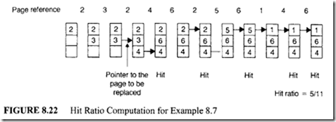
 

image

image

image

image

image

Example 7.1

If the following two instructions are to be added to the instruction set of Figure 7.54, write a symbolic microprogram for the CPU of section 7.3 that describes the execution of each instruction:

image

Nanomemory is another approach for reducing the size of the control memory. This technique contains a two-level memory: control memory and nanomemory. At the outset, are may feel that the two-level memory will increase the overall cost. In fact, it reduces the cost of the system by minimizing the memory size.

The concept of nanomemory is derived from a combination of horizontal and vertical instructions. However, this method provides trade-offs between them.

Motorola uses nanomemory to design the control units of their popular 16-bit and 32-bit microprocessors, including the 68000, 68020, 68030, and 68040. The nanomemory method provides significant savings in memory when a group of micro-operations occur several times in a microprogram. Consider the microprogram ofFigure 7.59, which contains A microinstructions B bits wide. The size of the control memory to store this microprogram is AB bits. Assume that the microprogram has n (n <A) unique microinstructions. These n microinstructions can be held in a separate memory called the "nanomemory" of size nB bits. Each of these n instructions occurs once in the nanomemory. Each microinstruction in the original microprogram is replaced with the address that specifies the location of the nanomemory in which the original B-bit-wide microinstructions are held.

Because the nanomemory has n addresses, only the upper integer of log2n bits is required to specify a nanomemory address. This is illustrated in Figure 7.60. The operation of microprocessor employing a nanomemory can be explained as follows: The microprocessor’s control unit reads an address from the microprogram. The content of this address in the nanomemory is the desired control word. The bits in the control word are used by the control unit to accomplish the desired operation. Note that a control unit employing nanomemory (two-level memory) is slower than the one using a conventional control memory (single memory). This is because the nanomemory requires two memory reads (one for the control memory and the other for the nanomemory). For a single conventional control memory, only one memory fetch is necessary. This reduction in control unit speed is offset by the cost of the memory when the same microinstructions occur many times in the microprogram.

Consider the 7 x 4-bit microprogram stored in the single control memory of Figure 7.61. This simplified example is chosen to illustrate the nanomemory concept even though this is not a practical example. In this program, 3 out of 7 microinstructions are unique.
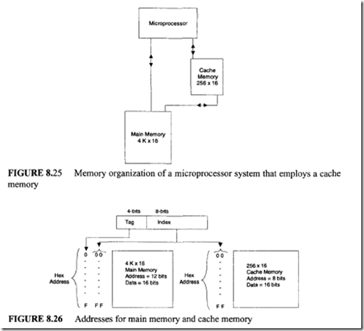
Therefore, the size of the microcontrol store is 7 x 2 bits and the size of the nanomemory is 3 x 4 bits. This is shown in Figure 7.62.

Memory requirements for the single control memory = 7 x 4 = 28 bits. Memory requirements for nanomemory = (7 x 2 + 3 x 4) bits = 26 bits. Therefore, the saving using nanomemory = 28 – 26 = 2 bits. For a simple example like this, 2 bits are saved.

The HMOS 68000 control unit nanomemory includes a 640 x 9-bit microcontrol store and a 280 x 70-bit nanocontrol store as shown in Figure 7.63. In Figure 7.63, out of640 microinstructions, 280 are unique. If the 68000 were implemented using a single control memory, the requirements would have been 640 x 70 bits. Therefore,

Memory savings = (640 x 70)- (640 x 9 + 280 x 70) bits

                     = 44,800- 25,360

                     = 19,440 bits

This is a tremendous memory savings for the 68000 control unit.