QUESTIONS AND PROBLEMS
7.1 It is desired to implement the following instructions using block code: ADD, SUB, XOR, MOVE, HALT. Draw a block diagram.
7.2 The instruction length and the size of an address field are 9 bits and 3 bits respectively. Is it possible to have
6 two-address instructions
15 one-address instructions
8 zero-address instructions
using expanding op-code technique? Justify your answer.
7.3 Using the instruction format of Problem 7.2, is it possible to have
7 two-address instructions
7 one-address instructions
8 zero-address instructions
using expanding opcode technique? Justify your answer.
7.4 Assume that it is desired to have 2 two-address, 7 one-address, and 25 zero address instructions in a computer instruction set. Using expanding op-code technique with a 2-bit op-code and 3-bit address field, is it possible to accomplish the above? If so, justify your answer and determine the instruction length.
7.5 Assume that using an instruction length of 9 bits and the address field size of 3 bits, 5 two-address and 10 one-address instructions have already been designed, using expanding op-code technique. Is it possible to have at least 48 zero-address instructions that can be added to the instruction set?
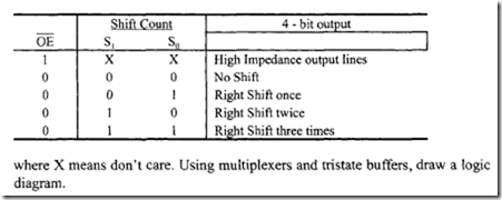
7.6 Design a combinational logic shifter with 4-bit input and 4-bit output as follows:
 7.7 Draw a logic diagram for a 4 x 4 barrel shifter.
7.8 Using a minimum number of full adders and multiplexers, design an incrementer/ decrementer circuit as follows: If S = 0, output y = x + I; otherwise, y = x – I. Assume x andy are 4-bit signed numbers and the result is 4 bits wide.
7.9 Design a combinational circuit to compute the absolute value of an 8-bit twos complement number. Use 8-bit binary adder and exclusive-OR gates. Draw a logic circuit.
7.10 Using a 4-bit CLA as the building block, design an 8-bit adder.
7.11 Design:
(a) a 16-bit adder whose worst-case add-time is 1Oil using a 4-bit CLA as a building block.
(b) the fastest 64-bit adder using a 4-bit CLA as the building block. Estimate the worst-case add-time of your design.
(c) a combinational circuit to compute the functionf(x) = (3/8) * x where x is a 4-bit 2’s complement number.
7.12 Design an arithmetic logic unit to perform the following functions:
 Use multiplexers, binary adders, and gates as needed. Assume that A and B are 4-bit numbers. Draw a logic circuit.
7.13 Design a combinational circuit that will perform the following operations:
 Assume that A is a 4-bit number and B =
![]() Draw a logic diagram.
Draw a logic diagram.
7.14 Design a 4-bit ALU to perform the following operations:
Assume that A is a 4-bit number. Draw a logic diagram using a binary adder, multiplexers, and inverters as necessary.
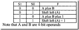
7.15 Design a 4-bit arithmetic unit as follows:
Assume that A and B are 4-bit numbers .
7.16 Design an ALU to perform the following operations:
 Assume that x andy are 4-bit numbers, and B=
 ![]() . Draw a logic diagram.
. Draw a logic diagram.
7.17 Assume two 2’s complement signed numbers, M= 111111112 and Q= 111111002 •
Perform the signed multiplication using the algorithm described in Section 7.2.2.
7.18 What is the purpose of the control unit in a microprocessor?
7.19 Draw a logic diagram to implement the following register transfers:
(a) If the content of the 8-bit register R is odd, then
 (b) If the number in the 8-bit register R is negative, then x –x- 1 else x <— x + 1. Assume x andy are 4 bits wide.
7.20 Discuss briefly the merits and demerits of single-bus, two-bus, and three-bus architectures inside a control unit.
7.21 What is the basic difference between hardwired control, microprogramming, and nanoprogramming? Name the technique used for designing the control units of the Intel 8086, Motorola 68000, and PowerPC.
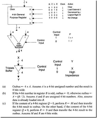
7.22 Using the following components: 4-bit general-purpose register, 4-bit adder/subtractor, and tristate buffer, and assuming the inbus and outbus are
4 bits wide, design a control unit using hardwired control to perform the following operations. You may use counters, decoders, and PLAs as required.
 7.23 Repeat Problem 7.22 using microprogramming.
7.24 Discuss the basic differences between microprogramming and nano programming.
7.25 (a) A conventional microprogrammed control unit includes 1024 words by 85 bits. Each of 512 microinstructions are unique. Calculate the savings if any by having a nanomemory. Calculate the sizes of microcontrol memory and nanomemory.
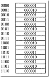
(b) Consider the following 14 x 6 microprogram using a conventional control memory:
Implement this microprogram in a nanomemory. Justify the use of either a single control memory or a two-level memory for the program.
7.26 Discuss the basic differences between CISC and RISC.
7.27 Design and implement a combinational circuit that will work as follows:
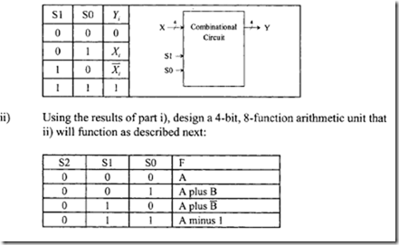
7.28 i) Design a combinational circuit that will satisfy the following specification.
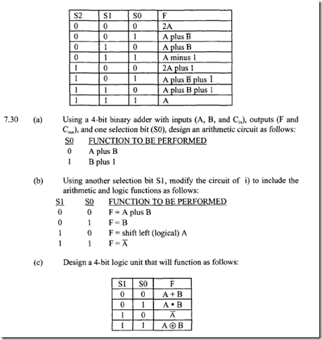
7.29 Design a 4-bit, 8-function arithmetic unit that will meet the following specifications:
7.31 Design and implement a 6 x 6 array multiplier.
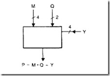
7.32 Design an unsigned 8 x 4 non-additive multiplier using additive-multiplier module whose block diagram representation is as follows:
Assume that M, Q, and Y are unsigned integers.
7.33 Using four 256 x 8 ROMS and 4-bit parallel adders, design a 8 x 8 unsigned, nonadditive multiplier. Draw a logic diagram of your implementation.
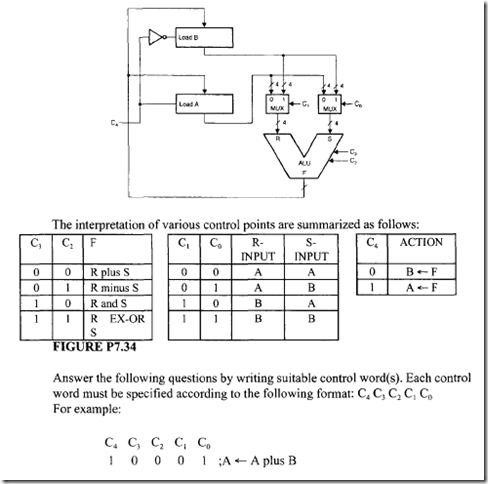
7.34 Consider the registers and ALU shown in Figure P7.34:
(a) How will the A register be cleared? (Suggest at least two possible ways.) DIRECT CLEAR input is not available.
(b) Suggest a sequence of control words that exchanges the contents of A and B registers (exchange means A Band B A).
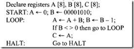
7.35 Consider the following algorithm:
Design a hardwired controller that will implement this algorithm.
7.36 It is desired to build an interface in order establish communication between a 32- bit host computer and a front end 8-bit microcomputer (See Figure P7.36). The operation of this system is described as follows:
Step 1: First the host processor puts a high signal on the line "want" (saying that it needs a 32-bit data) for one clock period.
Step 2: The interface recognizes this by polling the want line.
Step 3: The interface unit puts a high signal on the line "fetch" for one clock period (that is it instructs the microcomputer to fetch an 8-bit data).
Step 4: In response to this, the microcomputer samples the speech signal, converts it into an 8-bit digital data and informs the interface that the data is ready by placing a high signal on the "ready" line for one clock period.
Step 5: The interface recognizes this (by polling the ready line), and it reads the 8-bit data into its internal register.
Step 6: The interface unit repeats the steps 3 through 5 for three more times (so that it acquires 32-bit data from the microcomputer).
Step 7: The interface informs the host computer that the latter can read the 32-bit data by placing a high signal on the line "takeit" for one clock period.
Step 8: The interface unit maintains a valid 32-bit data on the 32-bit output bus until the host processor says that it is done (the host puts a high signal on the line "done" for one clock period). In this case, the interface proceeds to step 1 and looks for a high on the "want" line.
(a) Provide a Register Transfer Language description of the interface.
(b) Design the processing section of the interface.
{c) Draw a block diagram ofthe interface controller.
(d) Draw a state diagram of the interface controller.
7.37 Solve Problem 7.35 using the microprogrammed approach.
7.38 Design a microprogrammed system to add numbers stored in the register pair AB and CD. A, B, C, and D are 8-bit registers. The sum is to be saved in the register pair AB. Assume that only an 8-bit adder is available.
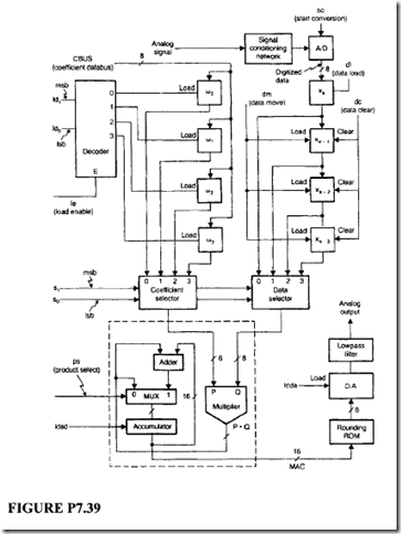
7.39 The goal of this problem is to design a microprogrammed 3rd order FIR (Finite impulse response) digital filter. In this system, there are 4 coefficients w0, w 1 , w2, and w3• The output Yk (at the kth clock period) is the discrete convolution product of the inputs (x ) and the filter coefficients. This is formally expressed as follows:
![]() In the above summation, xk represents the input at the kth clock period
In the above summation, xk represents the input at the kth clock period
whilexk-i represents input at (k- i)th sample period. For all practical purposes, we assume that our system is causal and so xi= 0 for i < 0. The processing hardware is shown in Figure P7.39. This unit includes 8 eight-bit registers (to hold data and coefficients), AID (Analog digital converter), MAC (multiplier accumulator), and a D/A (Digital analog converter). The processing sequence is shown below:
1 Initialize coefficient registers
2 Clear all data registers except xi
3 Start AID conversion (first make sc = I and then retract it to 0)
4 Wait for one control state (To make sure that the conversion is complete)
5 Read the digitized data into the register xk
6 Iteratively calculate filter output Yk (use MAC for this)
7 Pass Yk to D/A (Pass Accumulator’s output to DIA via Rounding ROM)
8 Move the data to reflect the time shift (x k- 3 = x k _ 2 , x k _ 2 = x k _ 1 , x k- 1 =x k)
9 Go to 3
(a) Specify the controller organization.
(b) Produce a well documented listing of the binary microprogram
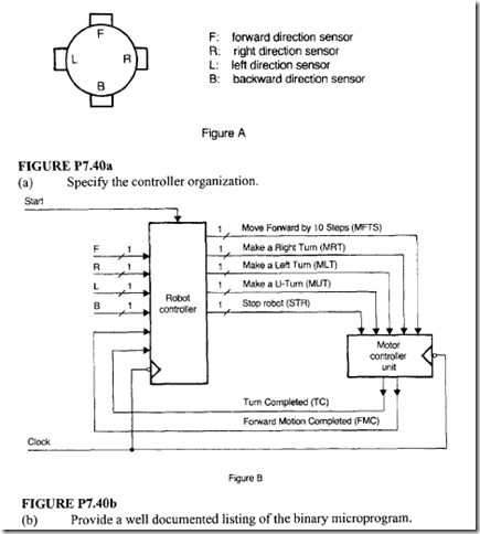
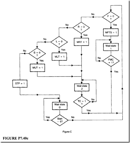
 7.40 Your task is to design a microprogrammed controller for a simple robot with 4 sensors (see Fig. A). The sensor output will go high only if there is a wall or an obstruction within a certain distance. For example, ifF= 1, there is an obstruction or wall in the forward direction. In particular, your controller is supposed to communicate with a motor controller unit shown in Fig. B. The flow chart that describes the control algorithm is shown in Fig. C. The outputs such as MFTS, MRT, MLT, MUT, and STP, andd the status signals such as FMC, and TC will be high for one clock period. Assume that a power on reset causes the controller to go the WAIT STATE 0.
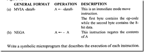
7.41 It is desired to add the following instructions to the instruction set shown in Figure 7.54.
7.42 Explain how the effect of an unconditional branch instruction of the following form is simulated:
JP <addr>
Use the instruction set shown in Figure 7.54.
7.43 Using the instruction set shown in Figure 7.54, write a program to add the contents of the memory locations 6416 through 6D 16 and save the result in the address 6E 16•
7.44 Show that it is possible to specify 675 microoperations using a 10 bit control function field.
7.45 A microprogram occupies 100 words and each word typically emits 70 control signals. The architect claims that by using a 2i x 70 nanomemory (for some i > 0), it is possible to save 4260 bits. If this were true, determine the number of distinct control states in the original microprogram (Note that here when we say a control state we refer only to the control function field).
Hint: You may have to employ a trial and error approach to solve this problem.


