7.4 Design of a Microprogrammed CPU
Next, the design of a microprogrammed processor is illustrated. The programming model of this processor is shown in Figure 7.52.
The CPU contains two registers:
1. An 8-bit register A 2. A 2-bit flag register F
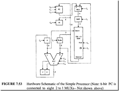
The flag register holds only zero (Z) and carry (C) flags. All programs and data are stored in the 256 x 8 RAM. The detailed hardware schematic of the data-flow part of this processor is shown in Figure 7.53.
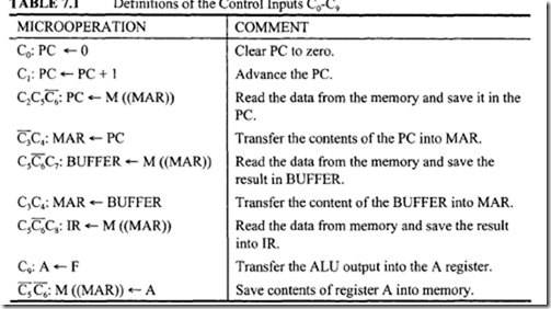
From Figure 7.53, it can be seen that the hardware organization includes four more 8-bit registers, PC, IR, MAR, and BUFFER. These registers are transparent to a programmer. The 8-bit register BUFFER is used to hold the data that is retrieved from memory. In this system, only a restricted number of data paths are available. These paths are controlled by the control inputs C0 through C9, as defined in Table 7.1.
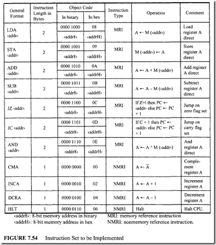
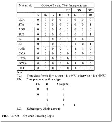
From Figure 7.54, notice that the proposed instruction set contains 11 instructions. The first 7 instructions are classified as memory reference instructions, since they all require a memory address (which is an 8-bit number in this case). The last 4 instructions do not require any memory address; they are called nonmemory reference instructions. Each memory reference instruction is assumed to occupy 2 consecutive bytes in the RAM. The first byte is reserved for the op-code, and the second byte indicates the 8-bit memory address. In contrast, a nonmemory reference instruction takes only one byte of storage. This instruction set supports only two addressing modes: implicit and direct. Both branch instructions are assumed to be absolute mode branch instructions. The op-code encoding for this instruction set is carried out in a logical manner, as explained in Figure 7.55.
The bit I3 of Figure 7.55 decides the instruction type. If I3 = 1, it is a memory reference
instruction (MRI), otherwise it is a nonmemory reference instruction (NMRI).
Within the memory reference category, instructions are classified into four groups, as follows:
 There are two instructions in the first three groups. Bit 10 is used to determine the desired instruction of a particular group. Iflo of group 0 equals zero, it is the load (LDA) instruction; otherwise it is the store (STA) instruction. Nevertheless, no such classification is required for group 3 and the nonmemory reference instructions.
As mentioned before, the instruction execution involves the following steps:
 The eight ALU operations performed by the CPU are defined by C10C11C12 as follows:
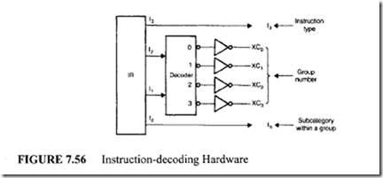
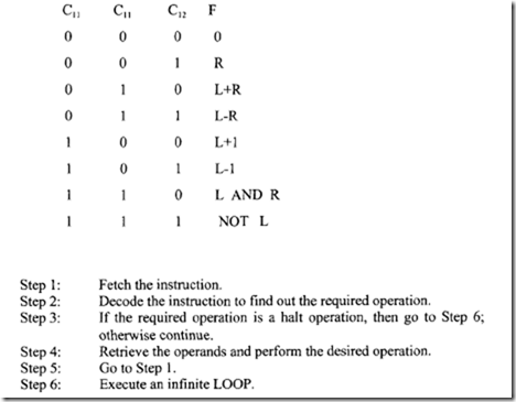 The first step is known as the fetch cycle, and the rest are collectively known as the execution cycle. To decode the instruction, the hardware shown in Figure 7.56 is used.
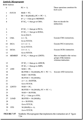
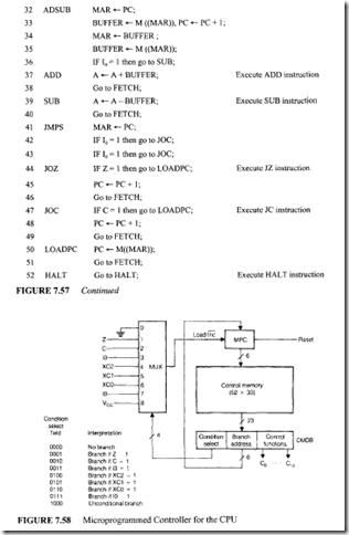
With this hardware and the status flags (Z and C), a microprogram to implement
the instruction set can be written. The symbolic version of this microprogram is shown in
The hardware organization of the microprogrammed control unit for this situation shown in Figure 7.58 directly follows the symbolic listing shown in Figure 7.57. No attempt has been made toward arriving at a minimal microprogram. Rather, the concept was presented. The task of translating the symbolic microprogram of Figure 7.57 into a binary microprogram is left as an exercise.
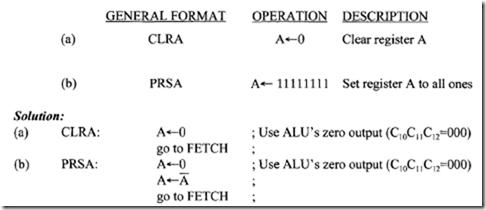
Example 7.1
If the following two instructions are to be added to the instruction set of Figure 7.54, write a symbolic microprogram for the CPU of section 7.3 that describes the execution of each instruction:
Nanomemory is another approach for reducing the size of the control memory. This technique contains a two-level memory: control memory and nanomemory. At the outset, are may feel that the two-level memory will increase the overall cost. In fact, it reduces the cost of the system by minimizing the memory size.
The concept of nanomemory is derived from a combination of horizontal and vertical instructions. However, this method provides trade-offs between them.
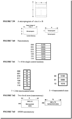
Motorola uses nanomemory to design the control units of their popular 16-bit and 32-bit microprocessors, including the 68000, 68020, 68030, and 68040. The nanomemory method provides significant savings in memory when a group of micro-operations occur several times in a microprogram. Consider the microprogram ofFigure 7.59, which contains A microinstructions B bits wide. The size of the control memory to store this microprogram is AB bits. Assume that the microprogram has n (n <A) unique microinstructions. These n microinstructions can be held in a separate memory called the "nanomemory" of size nB bits. Each of these n instructions occurs once in the nanomemory. Each microinstruction in the original microprogram is replaced with the address that specifies the location of the nanomemory in which the original B-bit-wide microinstructions are held.
Because the nanomemory has n addresses, only the upper integer of log2n bits is required to specify a nanomemory address. This is illustrated in Figure 7.60. The operation of microprocessor employing a nanomemory can be explained as follows: The microprocessor’s control unit reads an address from the microprogram. The content of this address in the nanomemory is the desired control word. The bits in the control word are used by the control unit to accomplish the desired operation. Note that a control unit employing nanomemory (two-level memory) is slower than the one using a conventional control memory (single memory). This is because the nanomemory requires two memory reads (one for the control memory and the other for the nanomemory). For a single conventional control memory, only one memory fetch is necessary. This reduction in control unit speed is offset by the cost of the memory when the same microinstructions occur many times in the microprogram.
Consider the 7 x 4-bit microprogram stored in the single control memory of Figure 7.61. This simplified example is chosen to illustrate the nanomemory concept even though this is not a practical example. In this program, 3 out of 7 microinstructions are unique.
Therefore, the size of the microcontrol store is 7 x 2 bits and the size of the nanomemory is 3 x 4 bits. This is shown in Figure 7.62.
Memory requirements for the single control memory = 7 x 4 = 28 bits. Memory requirements for nanomemory = (7 x 2 + 3 x 4) bits = 26 bits. Therefore, the saving using nanomemory = 28 – 26 = 2 bits. For a simple example like this, 2 bits are saved.
The HMOS 68000 control unit nanomemory includes a 640 x 9-bit microcontrol store and a 280 x 70-bit nanocontrol store as shown in Figure 7.63. In Figure 7.63, out of640 microinstructions, 280 are unique. If the 68000 were implemented using a single control memory, the requirements would have been 640 x 70 bits. Therefore,
Memory savings = (640 x 70)- (640 x 9 + 280 x 70) bits
= 44,800- 25,360
= 19,440 bits
This is a tremendous memory savings for the 68000 control unit.
