Cache Memory Organization
The performance of a microcomputer system can be significantly improved by introducing a small, expensive, but fast memory between the microprocessor and main memory. This memory is called "cache memory" and this idea was first introduced in the IBM 360/85 computer. Later on, this concept was also implemented in minicomputers such as the PDP-11/70. With the advent of VLSI technology, the cache memory technique is gaining acceptance in the microprocessor world. Studies have shown that typical programs spend most of their execution times in loops. This means that the addresses generated by a microprocessor have a tendency to cluster around a small region in the main memory, a phenomenon known as "locality of reference." Typical 32-bit microprocessors can execute the same instructions in a loop from the on-chip cache rather than reading them repeatedly from the external main memory. Thus, the performance is greatly improved. For example, an on-chip cache memory is implemented in Intel’s 32-bit microprocessor, the 80486/Pentium, and Motorola’s 32-bit microprocessor, the MC 68030/68040. The 80386 does not have an on-chip cache, but external cache memory can be interfaced to it.
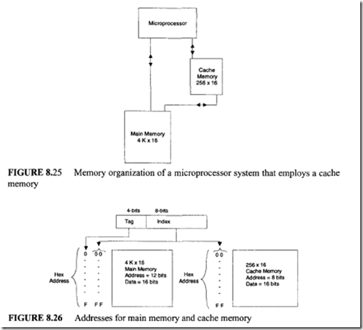
The block diagram representation of a microprocessor system that employs a cache memory is shown in Figure 8.25. Usually, a cache memory is very small in size and
its access time is less than that of the main memory by a factor of 5. Typically, the access times of the cache and main memories are 100 and 500 ns, respectively_ If a reference is found in the cache, we call it a "cache hit," and the information pertaining to the microprocessor reference is transferred to the microprocessor from the cache. However, if the reference is not found in the cache, we call it a "cache miss." When there is a cache miss, the main memory is accessed by the microprocessor and, the instructions and/or data are then transferred to the microprocessor from the main memory. At the same time, a block containing the desired information needed by the microprocessor is transferred from the main memory to cache. The block normally contains 4 to 16 words, and this block is placed in the cache using the standard replacement policies such as FIFO or LRU. This block transfer is done with a hope that all future references made by the microprocessor will be confined to the fast cache.
The relationship between the cache and main memory blocks is established using mapping techniques. Three widely used mapping techniques are Direct mapping, Fully associative mapping, and Set-associative mapping. In order to explain these three mapping techniques, the memory organization of Figure 8_26 will be used. The main memory is capable of storing 4K words of 16 bits each. The cache memory, on the other hand, can store 256 words of 16 bits each. An identical copy of every word stored in cache exists in main memory. The microprocessor first accesses the cache. If there is a hit, the microprocessor accepts the 16-bit word from the cache. In case of a miss, the microprocessor reads the desired 16-bit word from the main memory and this 16-bit word is then written to the cache. A cache memory may contain instructions only (Instruction cache) or data only (Data cache) or both instructions and data (Unified cache).
Direct mapping uses a RAM for the cache. The microprocessor’s 12-bit address is divided into two fields, an index field and a tag field. Because the cache address is 8 bits wide (28 = 256), the low-order 8 bits of the microprocessor’s address form the index field, and the remaining 4 bits constitute the tag field. This is illustrated in Figure 8.26.
In general, if the main memory address field ism bits wide and the cache memory address is n bits wide, the index field will then require n bits and the tag field will be (m – n) bits wide. The n-bit address will access the cache. Each word in the cache will include the data word and its associated tag. When the microprocessor generates an address for main memory, the index field is used as the address to access the cache. The tag field of
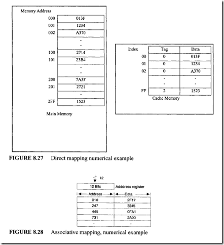
the main memory is compared with the tag field in the word read from cache. A hit occurs if the tags match. This means that the desired data word is in cache. A miss occurs if there is no match, and the required word is read from main memory. It is written in the cache along with the tag. One of the main drawbacks of direct mapping is that numerous misses may occur if two or more words with addresses having the same index but with different tags are accessed several times. This situation should be avoided or can be minimized by having such words far apart in the address lines. Let us now illustrate the concept of direct mapping for a data cache by means of a numerical example of Figure 8.27. All numbers are in hexadecimal.
The content of index address 00 of cache is tag= 0 and data= 013F. Suppose that the microprocessor wants to access the memory address 100. The index address 00 is used to access the cache. The memory address tag I is compared with the cache tag of 0. This does not produce a match. Therefore, the main memory is accessed and the data 2714 is transferred into the microprocessor. The cache word at index address 00 is then replaced with a tag of 1 and data of2714.
The fastest and the most expensive cache memory utilizes an associative memory. This method is known as "fully associative mapping." Each element in associative memory contains a main memory address and its content (data). When the microprocessor generates a main memory address, it is compared associatively (simultaneously) with all addresses in the associative memory. If there is a match, the corresponding data word is read from the associative cache memory and sent to the microprocessor. If a miss occurs, the main memory is accessed and the address along with its corresponding data are written to the associative cache memory. If the cache is full, certain policies such as FIFO are used as replacement algorithms for the cache. The associative cache is expensive but provides fast operation. The concept of an associative cache is illustrated by means of a numerical example in Figure 8.28. Assume all numbers are in hexadecimal.
The associative memory stores both the memory address and its contents (data).
The figure shows four words stored in the associative cache. Each word in the cache is the 12-bit address along with its 16-bit contents (data). When the microprocessor wants to access memory, the 12-bit address is placed in an address register and the associative cache memory is searched for a matching address. Suppose that the content of the microprocessor address register is 445. Because there is a match, the microprocessor reads the corresponding data OFA1 into an internal data register.
Set-associative mapping is a combination of direct and associative mapping. Each cache word stores two or more main memory words using the same index address. Each main memory word consists of a tag and its data word. An index with two or more tags and data words forms a set. When the microprocessor generates a memory request, the index of the main memory address is used as the cache address. The tag field of the main memory address is then compared associatively (simultaneously) with all tags stored under the index. If a match occurs, the desired data word is read. If a match does not occur, the
data word, along with its tag, is read from main memory and also written into the cache.
The hit ratio improves as the set size increases because more words with the same index but different tags can be stored in the cache. The concept of set-associative mapping can be illustrated by the numerical example shown in figure 8.29. Assume that all numbers are in hexadecimal.
Each cache word can store two or more memory words under the same index address. Each data item is stored with its tag. The size of a set is defined by the number of tag and data items in a cache word. A set size of two is used in this example. Each index address contains two data words and their associated tags.Each tag includes 4 bits, and each data word contains 16 bits. Therefore, the word length= 2 x (4 + 16) = 40 bits. An index address of 8 bits can represent 256 words. Hence, the size of the cache memory is 256 x 40. It can store 512 main memory words because each cache word includes two data words.
The hex numbers shown in Figure 8.29 are obtained from the main memory contents shown in Figure 8.27. The words stored at addresses 000 and 200 of main memory of figure 8.27 are stored in cache memory (shown in Figure 8.29) at index address 00. Similarly, the words at addresses 101 and 201 are stored at index address 01. When the microprocessor wants to access a memory word, the index value of the address is used to access the cache. The tag field of the microprocessor address is then compared with both tags in the cache associatively (simultaneously) for a cache hit. If there is a match, appropriate data is read into the microprocessor. The hit ratio will improve as the set size increases because more words with the same index but different tags can be stored in the cache. However, this may increase the cost of comparison logic.
There are two ways of writing into cache: the write-back and write-through methods. In the write-back method, whenever the microprocessor writes something into a cache word, a "dirty" bit is assigned to the cache word. When a dirty word is to be replaced with a new word, the dirty word is first copied into the main memory before it is overwritten by the incoming new word. The advantage of this method is that it avoids unnecessary writing into main memory.
In the write-through method, whenever the microprocessor alters a cache address, the same alteration is made in the main memory copy of the altered cache address. This policy can be easily implemented and also ensures that the contents of the main memory are always valid. This feature is desirable in a multiprocesssor system, in which the main memory is shared by several processors. However, this approach may lead to several unnecessary writes to main memory.
One of the important aspects of cache memory organization is to devise a method that ensures proper utilization of the cache. Usually, the tag directory contains an extra bit for each entry, called a "valid" bit. When the power is turned on, the valid bit corresponding to each cache block entry of the tag directory is reset to zero. This is done in order to indicate that the cache block holds invalid data. When a block of data is first transferred from the main memory to a cache block, the valid bit corresponding to this cache block is set to 1. In this arrangement, whenever the valid bit is zero, it implies that a new incoming block can overwrite the existing cache block. Thus, there is no need to copy the contents of the cache block being replaced into the main memory.
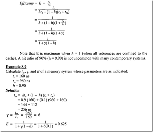
The performance of a system that employs a cache can be formally analyzed as follows: If tc, h, and t., specify the cache-access time, hit ratio, and the main memory access time, respectively; then the average access time can be determined as shown in the equation below:
![]() The hit ratio h always lies in the closed interval 0 and 1, and it specifies the relative number of successful references to the cache. In the above equation, when there is a cache hit, the main memory will not be accessed; and in the event of a cache miss, both main memory and cache will be accessed. Suppose the ratio of main memory access time to cache access time is y, then an expression for the efficiency of a system that employs a cache can be derived as follows:
The hit ratio h always lies in the closed interval 0 and 1, and it specifies the relative number of successful references to the cache. In the above equation, when there is a cache hit, the main memory will not be accessed; and in the event of a cache miss, both main memory and cache will be accessed. Suppose the ratio of main memory access time to cache access time is y, then an expression for the efficiency of a system that employs a cache can be derived as follows:
This result indicates that by employing a cache, efficiency is improved by 62.5%. Assume the unit of mapping is a block; then the relationship between the main and cache memory blocks can be established by using a specific mapping technique.
In fully associative mapping, a main memory block i can be mapped to any cache blockj, where 0:%; i:%; M -1 and 0:%; j:%; N- 1 Note that the main memory has M blocks and the cache is divided into N blocks. To determine which block of main memory is stored into the cache, a tag is required for each block. Hence, Tag ( j ) = address of the main memory block stored in the cache block j.
Suppose M = 2m and N = 2n; then m and n bits are required to specify the addresses of a main and cache memory block, respectively. Also, block size = 2w, where w bits are required to specify a word in a block.
For Associative mapping : m bits of the main memory are used as a tag; and N tags are needed since there are N cache blocks.
Main memory address= (Tag+ w)bits.
For Direct mappin2: High order (m-n) bits are used as a tag.
Main memory address= (Tag+ n + w)bits
For Set-associative mappin2:
Tag field= (m- n + s) bits, where Blocks/set= 2′ Cache set number = (n – s) bits Main memory address = (Tag size + cache set number+ w ) bits.
Example 8.10
The parameters of a computer memory system are specified as follows:
-
Main memory size = 8K blocks
-
Cache memory size =512 blocks
-
Block size = 8 words
Determine the sizes of the tag field along with the main memory address using each of the following methods:
(a) Fully associative mapping
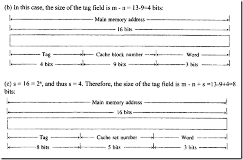
(b) Direct mapping
(c) Set associative mapping with 16 blocks/set
Solution
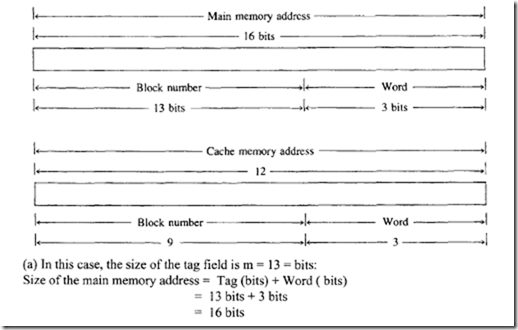
With the given data, compute the following:
-
M = 8K = 8192 = 2 13, and thus m = 13.
-
N = 512 = 29 , and thus n = 9.
-
Block size= 8 words= 23 words, and thus we require 3 bits to specify a word within a block.
Using this information, we can determine the main and cache memory address formats as shown next:
Examole 8.11
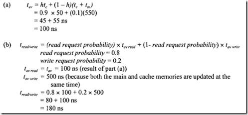
The access time of a cache memory is 50 ns and that of the main memory is 500 ns. It is estimated that 80% of the main memory requests are for read and the remaining are for write. The hit ratio for read access only is 0.9 and a write-through policy is used.
(a) Determine the average access time considering only the read cycles.
(b) What is the average time if the write requests are also taken into consideration
Solution
The growth in I C technology has allowed manufacturers to fabricate a cache on the CPU chip. The on-chip cache of Motorola’s 32-bit microprocessor, the MC68020, is discussed next.
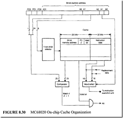
The MC68020 on-chip cache is a direct mapped instruction cache. Only instructions are cached; data items are not. This cache is a collection of 64 entries, where each cache entry consists of a 26-bit tag field and 32-bit instruction data. The tag field
includes the following components:
-
High-order 24 bits of the memory address.
-
The most-significant bit FC2 of the function code. In the MC68020 processor, the 3-bit function code combination FC2 FC 1 FCO is used to identify the status of the processor and the address space (discussed in Chapter 10) of the bus cycle. For example, FC2 = 1 means the processor operates in the supervisory or privileged mode. Otherwise, it operates in the user mode. Similarly, when FC 1 FCO = 0 I, the bus cycle is made to access data. When FC 1 FCO = 10, the bus cycle is made to access code.
-
Valid bit.
A block diagram of the MC68020 on-chip cache is shown in Figure 8.30.
If an instruction fetch occurs when the cache is enabled, the cache is first checked to determine if the word requested is in the cache. This is achieved by first using 6 bits of the memory address (A7-A2) to select one of the 64 entries of the cache. Next, address bits A31-A8 and function bit FC2 are compared to the corresponding values of the selected cache entry. If there is a match and the valid bit is set, a cache hit is occurs.
In this case, the address bit AI is used to select the proper instruction word stored in the cache and the cycle ends. If there is no match or the valid bit is cleared, and a cache miss occurs. In this case, the instruction is fetched from external memory. This new instruction is automatically written into the cache and the valid bit is set. Since the processor always pre fetches instructions from the external memory in the form of long words, both instruction data words of the cache will be updated regardless of which word caused the miss.
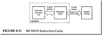
The MC68020 on-chip instruction cache obtains a significant increase in performance by reducing the number of fetches required to external memory. Typically, this cache reduces the instruction execution time in two ways. First, it provides a two clock-cycle access time for an instruction that hits in the cache (see Figure 8.31); second, if the access hits in the cache, it allows simultaneous instruction and data access to occur. Of these two benefits, simultaneous access is more significant, since it allows 100% reduction in the time required to access the instruction rather than the 33% reduction afforded by going from three to two clocks.
Finally, microprocessors such as Intel Pentium II support two-levels of cache. These are L1 (Levell) and L2 ( Level2) cache memories. The Ll cache (Smaller in size) is contained inside the processor chip while the L2 cache ( Larger in size) is interfaced external to the microprocessor. The Ll cache normally provides separate instruction and data caches. The processor can directly access the L1 cache while the L2 cache normally supplies instructions and data to the L I cache. The L2 cache is usually accessed by the microprocessor only if L1 misses occur. This two-level cache memory enhances the performance of the microprocessor.
