8155/8156: Programmable I/O Ports and Timer
1. In what way 8155 and 8156 differs?
Ans. The Chip Enable (CE) signal is active low for 8155, whereas it is active high for 8156.
2.What are the essential features of 8155.
Ans. The essential features of 8155 are
*8-bit 256 word RAM memory
*Two programmable 8-bit I/O port
* One programmable 6-bit IO port
*One programmable 14-bit binary Timer/Counter
* An internal address latch
*A control/status (C/S) register
* An internal decoder.
3. Functionally, how many sections are there in 8155?
Ans. Functionally, it has two sections—(a) a R/W memory and (b) programmable I/O and timer section.
4. Is it necessary to demultiplex the lower order bus AD7 –AD0 externally for 8155 to be connected to 8055?
Ans. No, it is not. This is because ALE, IO/ M , RD and WR signals of 8085 can be connected directly with 8155.
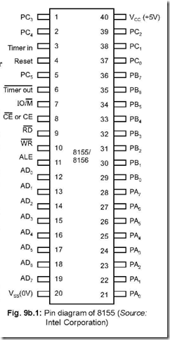
5. Draw the pin diagram of 8155.
Ans. The pin diagram of 8155 is shown in Fig. 9b.1.
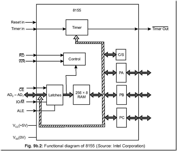
6. Draw the functional block diagram of 8155.
Ans. The functional block diagram of 8155 is shown in Fig. 9b.2 :
7. How the different ports, control/status register, timers are accessed? Write their addresses also.
Ans. The different combinations on the address lines A2, A1, A0 select one of the above, as shown:
|
A2 0 |
A1 0 |
A0 0 |
==>> |
Control/Status Register |
|
0 |
0 |
1 |
===>> |
Port A |
|
0 |
1 |
0 |
===>> |
Port B |
|
0 |
1 |
1 |
===>> |
Port C |
|
1 |
0 |
0 |
===>> |
LSB Timer |
|
1 |
0 |
1 |
===>> |
MSB Timer |
The other five (viz., A7 to A3) on the address lines are as: 0 0 1 0 0. Thus
|
A7 0 |
A6 0 |
A5 1 |
A4 0 |
A3 0 |
A2 0 |
A1 0 |
A0 0 |
===>> |
Address 20H |
— |
Register/Port/Timer Control/Status register |
|
0 |
0 |
1 |
0 |
0 |
0 |
0 |
1 |
===>> |
21H |
— |
Port A |
|
0 |
0 |
1 |
0 |
0 |
0 |
1 |
0 |
===>> |
22H |
— |
Port B |
|
0 |
0 |
1 |
0 |
0 |
0 |
1 |
1 |
===>> |
23H |
— |
Port C |
|
0 |
0 |
1 |
0 |
0 |
1 |
0 |
0 |
===>> |
24H |
— |
LSB timer |
|
0 |
0 |
1 |
0 |
0 |
1 |
0 |
1 |
===>> |
25H |
— |
MSB timer |
It is to be noted that the control/status register is having the same address 20H, but
the control register is accessed with WR = 0 and RD = 1. For status register access, WR
= 1 and RD = 0. The control register can never be read. For any future reference, the
control register content is stored in some accessible memory location.
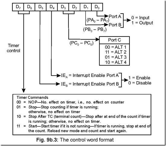
8. Draw the control word format and discuss the same in detail.
Ans. The control word loaded in the control register configures the different ports and the timer of 8155. The control word format is shown below:
The control register contains eight latches. The content of the lower 2 bits, viz., D1 – D0 configure ports A and B as input/output. Bits D3 and D2 configure bits PC0 – PC5 of port C (Port C is a 6-bit port while ports A and B both are of 8-bits) and can have four combinations—ALT1, ALT2, ALT3, ALT4 depending on the combinations of D3 and D2. Bits D5 and D4 are enable/disable pins for ports A and B respectively which enable/ disable the internal flip-flop of 8155. Bits D7 and D6 contain the timer commands.
As already mentioned, combinations of D3 – D2 bits give rise to ALT1 to ALT4 modes, which assigns port C bits in different configurations and shown below:
Table 9b.1: Port C pin assignment (Source: Intel Corporation)
|
Pin |
ALT1 |
ALT2 |
ALT3 |
ALT4 |
|
PC0 PC1 PC2 PC3 PC4 PC5 |
Input Port Input Port Input Port Input Port Input Port Input Port |
Output Port Output Port Output Port Output Port Output Port Output Port |
A INTR (Port AInterrupt) A BF (Port A Buffer Full) A STB(Port A Strobe) Output Port Output Port Output Port |
A INTR (Port A Interrupt) A BF (Port A Buffer Full) A STB(Port A Strobe) B INTR (Port B Interrupt) B BF (Port Buffer Full) B STB(Port B Strobe) |
ALT1 and ALT2 correspond to simple input/output of Port C respectively. In ALT3 mode, PC0 – PC2 bits are used as control signals for port A, while pins PC3 – PC5 act as output pins. In ALT4 mode, PC0 – PC2 bits are used as control signals for port A, while PC3 – PC5 bits are used as control signals for port B.
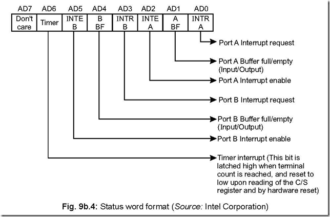
9. Draw the status word format and discuss the same. Ans. The status word format of 8155 is given below:
It has seven latches. Bit D7 is the ‘don’t care’ bit. Bit D6 contains the status of the timer. Bits D5 – D3 pertain to status of port B while bits D2 – D0 to that of Port A.
10. Discuss the timer section of 8155 and discuss its operating modes.
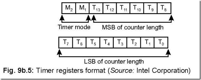
Ans. The timer section consists of two 8-bit registers. 14-bits of the two registers comprise to specify the count of the timer, which counts in a count-down manner. Contents of bits 6 and 7 of the most significant byte of the register decide the mode of operation of the counter. The following shows the timer register format. The timer section needs a ‘TIMER IN’ pulse, which is fed via pin 3 of 8155. A square wave or a pulse
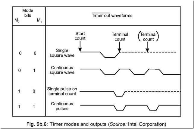
is obtained via pin 6 (TIMER OUT) when the terminal count (TC) is reached. The maximum and minimum values of the count down timer are 3FFH and 002H respectively. A single square wave or a continuous square wave or a single pulse
on TC or a pulse on each TC (i.e., continuous pulses) are obtained, depending on the mode setting bits M2 and M1.
The following figure shows the nature of the outputs for the different modes.
11. What happens when a high is applied on RESET ?
Ans. A high reset input resets the counter. To restart counting after resetting, a START command is required through the control register.
Thank you. This is so useful for me