Programming Techniques
1. Explain DAA instruction.
Ans. It stands for ‘decimal adjust accumulator’.
Execution of DAA instruction converts the content of the accumulator into two BCD
values. The system utilises the AC flag (not accessible by the programmer, but is used
internally for DAA operation) for this conversion by following the procedures stated below:
(a) If the lower order 4-bits (D3 – D0) of the accumulator is greater than 910 or if the AC flag is set, then this instruction (i.e., DAA) adds 0610 to the low-order 4-bits.
(b) If the higher order 4-bits (D7 – D4) of the accumulator is greater than 910 or if the CY flag is set, then this instruction (i.e., DAA) adds 6010 to the high-order 4-bits.
Examples follow to explain the above:
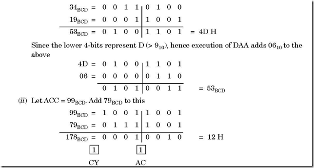
(i) Let ACC contains 34BCD. Add 19BCD to this
Here both higher order (0001) and lower order (0010) 4-bits are less than 910, but both AC and CY flags are set. Thus, DAA instruction execution will add 6610 to the result.
|
12 = |
0 |
0 |
0 |
1 |
0 |
0 |
1 |
0 |
|
|
66 = |
0 |
1 |
1 |
0 |
0 |
1 |
1 |
0 |
|
|
0 |
1 |
1 |
1 |
1 |
0 |
0 |
0 |
= 78BCD |
and since CY is already set, thus the answer is 178BCD.
2. What happens when HLT is executed in software?
Ans. All the buses go into the tri-state on execution of HLT instruction.
3. Write down the instructions that load H-L register pair by the contents of memory location 3500 H. Then move the contents to register C.
Ans. The corresponding instructions are
LXI H, 3500 H execution of this instruction loads H-L register pair with the contents of memory location 3500 H.
and MOV C, M execution of this instruction moves the contents of memory location 3500 H to register C.
4. Explain the two instructions (a) LDAX and (b) STAX
Ans. (a) The instruction LDAX indicates that the contents of the designated register pair point to a memory location and copies the contents of the memory location into the accumulator.
As an example, let D = 40 H, E = 50 H and memory location 4050 H = AB H. Then LDAX D transfers the contents of memory location 4050 H to the accumulator. Thus, after the execution of instruction, ACC = AB H
(b) STAX stands for ‘store accumulator indirect’. The contents of the accumulator are copied into the memory location specified by the contents of the register pair.
As an example, let D = 40 H and E = 50 H and ACC = AB H. Then STAX D stores the accumulator contents in the memory location 4050 H.
5. Explain the instructions (a) SHLD (b) LHLD.
4050 = AB H
Ans. (a) It stands for ‘Store H and L registers direct’. The instruction SHLD is followed by a 2-byte address. The content of L is stored in this address and the content of H is stored in the memory location that follows.
As an example, let H = 40 H and L = 50 H. Then execution of SHLD 6555 H stores 50 H in memory location 6555 H and 40 H is stored in 6556 H memory address.
(b) It stands for ‘Load H and L registers direct’.
It copies the contents of the memory location (that follows an LHLD instruction) into
L register and copies the contents of the next memory location in H register. The
contents of the two accessed memory locations remain unaltered.
As an example, let the memory location 3100 H and 3101 H contain 07 H and AF H
respectively. Then execution of LHLD 3100 H copies the content of 3100 H into L
and that of 3101 H into H register.
6. Memory location 3050 H is specified by HL pair and contains data FE H. Accumulator contains 14 H. Add the contents of memory location with accumulator. Store the result in 2050 H.
Ans. The program is written as follows:
LXIH, 3050 H fi HL register pair points 3050 H memory location
ADD M fi Add contents of 3050 H with accumulator
STA 2050 H fi Result in accumulator is stored in 2050 H
Prior to execution of the program, memory location 3050 H is loaded with data
FE H and accumulator with 14 H.
7. What the instruction DCR M stands for?
Ans. Here the memory location M is pointed to by the content of HL register pair. On executing DCR M, the content of the memory location is decremented by 01. Thus, if the memory location, as pointed to by HL register pair is AB H, then DCR M makes the content of that memory location to be AA H.
8. What the instruction DAD H stands for?
Ans. On executing the DAD H, the content of HL register pair is multiplied by 2. As an example if
9. Explain the two instructions (a) RAR and (b) RRC. Ans. (a) RAR stands for ‘rotate accumulator right through carry’.
Let the accumulator content = 95 H and carry flag = 0. Then execution of RAR will
change the contents of CY flag and accumulator as follows:
Bit D0 is placed in CY flag and the bit in the CY flag is placed in D7.
(b) RRC stands for ‘rotate accumulator right’.
Let, accumulator content = 95 H and carry flag = 0. Then execution of RRC will change the contents of CY flag and accumulator as follows:
Bit D0 is placed in D7 as well as in CY flag.
10. Explain the two instructions (a) RAL (b) RLC.
Ans. (a) RAL stands for ‘rotate accumulator left through carry’.
Let accumulator content = 95 H and carry flag = 0. Then execution of RAL will change the contents of CY flag and accumulator as follows:
Here D7 is placed in CY flag and the bit in CY flag placed in D0
(b) RLC stands for ‘rotate accumulator left’.
Let accumulator content = 95 H and carry flag = 0. Then execution of RLC will change the contents of CY flag and accumulator as follows:
11. Explain the instruction SPHL.
Ans. It stands for ‘Copy H and L registers to the stack pointer’.
This instruction copies the contents of H and L registers into the stack pointer register. The content of H register goes to the high order address and the content of L register to the low order address of SP. H and L register contents remain unchanged.
Let H = 31 H and L = 32 H before the instruction is executed. Hence after its execution, it would be like as follows:
12. Explain the instruction PCHL.
Ans. It stands for ‘load program counter (PC) with HL contents’. The contents of H and L are copied into higher and lower order bytes of the PC. H and L register contents remain unchanged.
Let H = 31 H and L = 32 H before the instruction is executed. Hence after its execution, it would be as follows:
13. Write down the result of EX–OR operation on accumulator and register B. Assume ACC = 18 H and B = 27 H.
Ans. The instruction used for this operation is XRA B.
|
ACC |
= |
0 |
0 |
0 |
1 |
1 |
0 |
0 |
0 |
|
B |
= |
0 |
0 |
1 |
0 |
0 |
1 |
1 |
1 |
|
EX–OR |
fi = |
0 0 3F H |
1 |
1 |
1 |
1 |
1 |
1 |
The result 3F H of EX–OR is stored in accumulator.
14. Consider the following:
Contents of H, L and SP registers are A0 H, B2 H and 3062 H. Memory locations 3062 H and 3063 H contain 52 H and 16 H respectively. Indicate the contents of these registers after XTHL operation.
Ans. XTHL stands for exchange H and L with top of stack.
Different Register contents before XTHL instruction
After XTHL instruction is carried out, the different register contents would be
15. Bring out the difference between arithmetic shift and logical shift.
Ans. An example, with a right shift, will be considered to bring out the difference between arithmetic shift and logical shift operations.
Let the accumulator content is
Then arithmetic right shift operation will make the contents of ACC as follows:
i.e., the sign bit of the original number is retained at the MSB place.
While logical right shift operation makes the ACC contents as follows:
i.e., the bits are shifted one bit position to the right.
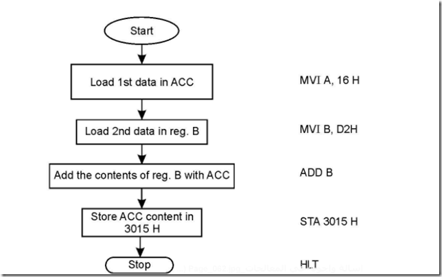
16. Draw the flow chart and write down the program to add two numbers 16 H and D2 H. Store the result in memory location 3015 H.
Ans. The flowchart for the above would look as follows.
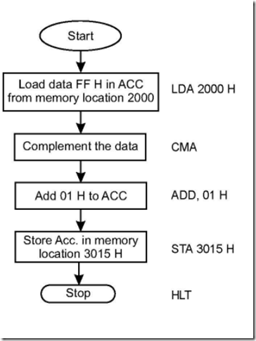
17. Write a program, along with flowchart, to find the 2’s complement of the number FF H, stored at memory location 2000 H. Store the result in memory location 3015 H.
Ans. The flowchart, along with the program, is shown below:
Memory location 2000 H contains data FF H.
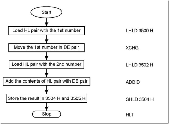
18. Write down the program to add two sixteen bit numbers. Draw the corresponding flowchart also.
Ans. Let the two sixteen bit numbers are stored at memory locations 3500 H to 3503 H. The result of addition is to be stored at memory locations 3504 H and 3505 H. The flowchart and the program will look like as follow:
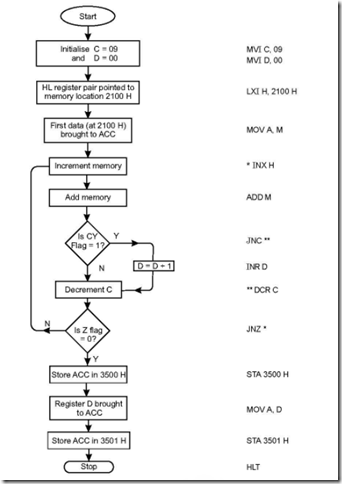
19. Ten 8-bit numbers are stored starting from memory location 2100 H. Add the numbers, store the result at 3500 H memory location and carry at 3501 H. Draw the flowchart also.
Ans. Initially, C register is stored with 09 H to take care of ten 8-bit data. Register D is initialised to 00 and stores the subsequent carry as addition is carried on. Final sum is stored at 3500 H while carry is stored at 3501 H.
The corresponding flowchart is also shown. Ten numbers of 8-bit data are stored starting from memory location 2100 H.
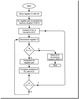
20. Ten 8-bit numbers are stored starting from memory location 3100 H. Find the greatest of the ten numbers and store it at memory location 3500 H.
Ans. Initially, D register is stored with 0A H—the number of data to be compared. The flowchart and the corresponding program are shown below:
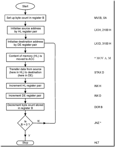
21. Ten number 8-bit data are stored starting from memory location 2100 H. Transfer this entire block of data to memory location starting from 3100 H.
Ans. B register is used here as a counter which stores the number of data bytes to be transferred. The flowchart along with the program are shown below:
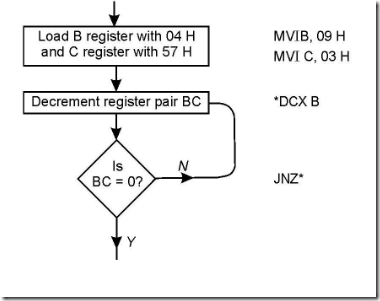
22. Set up a delay of 10 ms. Assume 3 MHz to be the microprocessor clock frequency.
Ans. Time delay is very easily generated by using a register (or a register pair— depending on the delay amount). Here the register pair BC is used to generate the delay with B loaded with 09 H and C with 03 H (calculations shown later). The flowchart and the program are shown side by side.
Calculations: A 3 MHz system clock corresponds to a time period of 0.3 ms. The
instructions MVI B, MVI C, DCX B and JNZ take 7, 7, 6 and 7 T-states respectively, of
which the two MVI instructions are outside the loop.
Time to execute MVI B and MVI C instructions.
= (7 + 7) × 0.3 ms
If the program loops n times, then time required for n loops
= time for 1 l.oop × n
= (6 + 7) × 0.3 × n
Thus 10 × 103 = (7 + 7) × 0.3 + (6 + 7) × 0.3 × n; fi n ª 2307)10 = 0903)H
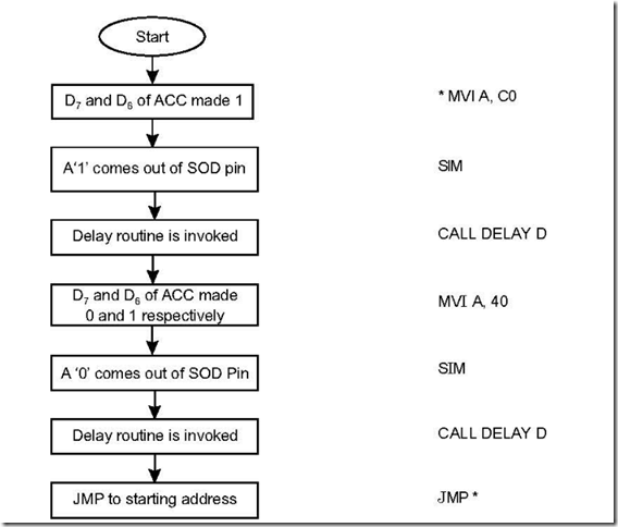
23. Generate a square wave of 50% duty cycle through the SOD pin of 8085. Ans. To generate a square wave, help of SIM instruction is taken. It reads like this
Thus, for a ‘1’ to come out of SOD pin, D7 and D6 of accumulator to be made 1 while for a ‘0’ to be taken out of SOD pin, D7 and D6 of accumulator to be made 0 and 1 respectively. In both the above cases, D5 to D0 (six bits in all) are to be put to 0. Thus the program reads like this:
Thus the above generates a square wave which is obtained through SOD pin of microprocessor, having time period of 2D (2 × delay time).
If a non 50% duty cycle is desired, then the two delays are made different, as desired.
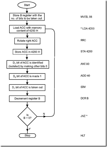
24. A data byte is stored in memory location 4200 H. This eight bit data is to be taken out of SOD pin, bit wise.
Ans. The flowchart and the program are as follows:
