8279: Programmable Keyboard/Display Interface
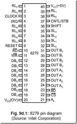
1. Draw the pin diagram of 8279.
Ans. The pin diagram of 8279 is shown below:
Fig. 9d.1: 8279 pin diagram (Source: Intel Corporation)
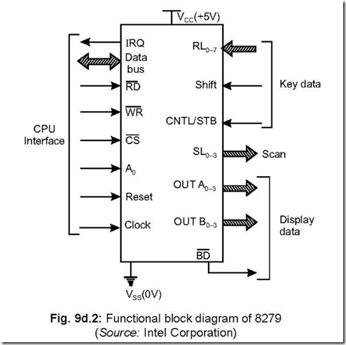
2. Draw the functional block diagram of 8279 and elaborate on the different blocks. Ans. The functional block diagram of 8279 is shown below:
The different functional blocks of 8279 are (a) a CPU interface, (b) a set of scan lines,
(c) input lines for key data and (d) output lines for display data.
The CPU interface consists of 8-bit data bus along with CS , RD , WR , CLK, RESET
and IRQ lines. IRQ is an output line which becomes 1 (active) when key data exists in an internal RAM of 8279. This line is normally connected to one of the hardware interrupt
Fig. 9d.2: Functional block diagram of 8279 (Source: Intel Corporation)
lines of the CPU. A high on A0 indicates that the signals in/out pertain to command/ status while a low on A0 indicate that they are data.
The scan lines (SL0–3) along with the eight return lines (RL0–7) can be used for construction of a keyboard matrix. SHIFT and CNTL/STB signals (both inputs) contribute the characteristics for individual keys.
The display output is available through A0–3 and B0–3 which can be used together as
an 8-bit port. BD (output signal) is used for display blanking purposes.
3. What are the two most important functions performed by 8279? Ans. The two most important functions performed by 8279 are as follows:
(a) It scans the keyboard, then detects the key press and transmits to the CPU information which corresponds to the particular key pressed.
(b) It puts out data received from the CPU, for use by the display devices.
4. What are the various input modes in which 8279 operate? Ans. There are three input modes in which 8279 operates:
z Scanned Keyboard Mode
z Scanned Sensor Matrix Mode
z Strobed Input Mode.
5. How many character definitions are possible using 8279? Ans. A maximum of 256 character definitions are possible using 8279.
6. When the CPU is actually involved for the scan and display functions to be realised?
Ans. For the above two functions to be realised, CPU involvement is required only when data is actually transmitted to or received from the CPU.
7. What are the modes in which the four scan lines can operate?
Ans. The four scan lines (SL0 – SL3) can be operated in two modes—encoded and decoded mode.
8. Discuss the encoded and decoded mode.
Ans. Encoded mode: Here 16 lines are generated using the 4 scan lines and a 4 to 16 external decoder, although the manufacturers recommend not to use the SL3 line. Thus eight decoded scan lines are possible with SL0 – SL2 lines and a 3 to 8 decoder. These 8 lines, along with eight return lines (RL0 – RL7) can form a 8 × 8 keyboard matrix. Thus it leads to 64 different character definitions. With SHIFT and CONTROL input lines taken as two additional input lines, total character definitions possible = 64 × 22 = 256.
Decoded mode: Using the internal decoder present in 8279, SL0–SL3 lines are decoded. With SHIFT and CONTROL lines along with RL0 – RL7 lines, total character definition possible here is = 4 × 8 × 4 = 128.
9. Describe the Scanned Keyboard Mode.
Ans. Both encoded and decoded scan versions are applicable in this case. This mode can be divided into two ways.
z 2 key lockout
z N-key rollover
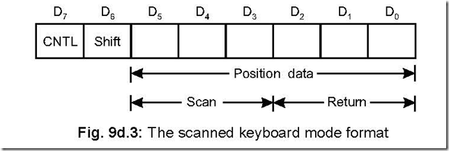
In this mode, the pressing of a key generates a unique 6-bit data (called ‘position data’) which is characteristic of the position of the key pressed. These 6-bits, along with CNTL and SHIFT form a 8-bit word, shown below. Of the position data D5 – D0, Scan bits correspond to D5 – D3 and Return bits correspond to D2 – D0. D5 – D3 bits correspond to the position of the row on which the key is pressed while D2 – D0 correspond to the position of the column on which the key is pressed. This 8-bit word gets stored in the RAM of 8279 (in FIFO order) and consequently the IRQ (interrupt request, an output line) line goes high. This IRQ line is connected to one of the hardware interrupt pins of the CPU. On recognition of the interrupt input by the CPU, the RAM in 8279 is read in FIFO form. Once this reading by CPU is over IRQ line of 8279 goes low but will become high if the RAM contains another data.
2 Key Lockout: In this 2 key lock out version of Scanned Keyboard Mode, when any key is pressed, it waits for next two scans to check whether any other key is pressed or not. Several possibilities do arise which need to be addressed separately.
(a) No other key press is detected. Then data corresponding to key press is taken to RAM in 8279 and IRQ output line goes into high state.
In case this internal RAM (of 8279) is already full, the keyed data is ignored and the error flag is set (= 1).
(b) If one or more additional key pressing occurs, no data entry into RAM is allowed. In this case two possibilities occur:
(i) If the first key (i.e., the key which was pressed first) is released ahead of others, then the key press is ignored.
(ii) If all the keys are released before the key first pressed, then data corresponding to first key pressed, is entered into RAM of 8279.
Another possibility is pressing of two keys within one debounce cycle (the time required for eliminating contact bounce effect is known as contact debounce time). In this case, no key is recognised. When one key is released, the other key that remains pressed is recognised as a single valid key depression.
N-Key Rollover: In this case, the debounce circuit waits for two scans after the first key press. It then checks whether key is still in the pressed condition or not. If the answer is yes, then the data corresponding to the key press is taken into RAM of 8279. No limit is there to the number of key presses. For simultaneous key presses, data are entered according to the order of key press.
If within a single debounce cycle, two keys are found pressed, the error flag is set
and data entry into the RAM is prohibited. The error flag can be read from the FIFO STATUS word and can be cleared by a CLEAR command (CF = 1).
10. Describe the Scanned Sensor Matrix Mode.
Ans. In the Scanned Sensor Matrix Mode of operation, the keys are arranged in the form of a matrix, with the scan lines (SL0 – SL2) forming the columns and return lines (RL0 – RL7) forming the rows. The open/closed condition of the key is stored in a RAM location. The size of the matrix be 8 × 8 or 4 × 8 for encoded and decoded scan lines respectively.
The data entering via the RL lines are admitted into eight columns of the sensor RAM—thus each RAM position corresponds to a specific switch position. Apart from switches, other logic circuit output lines can be connected to the RL lines.
11. Describe the Strobed Input Mode.
Ans. In this mode, data are placed on the return lines (RLs). The source of data may be an encoded keyboard or a switch matrix. The data so entering go to FIFO RAM and are accepted on the rising edge of a CNTL/STB pulse.
12. State the options available in the display mode. Ans. The available options are:
z Display format—either left entry (also known as typewriter mode), or right entry (also
known as calculator mode).
z Number of display characters: eight or sixteen.
z Organisation of characters—Single 8-bit or dual 4-bit type.
13. Discuss the Left Entry (Typewriter) Mode of Display format.
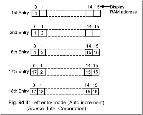
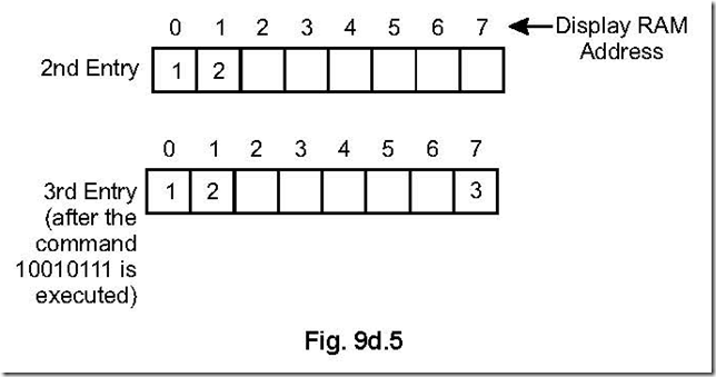
Ans. In the left entry (or typewriter) mode, the first entry goes to address 0, the second entry to address 1 and so on. The first entry goes to the left most display position. The second entry to the just right of the earlier one. Thus the 16th entry goes to 15th address position. It is to be remembered that the 17th entry goes to the RAM address 0 again, 18th entry goes to RAM address 1 etc, and is shown in Fig. 9d.4.
In this mode, data can be entered at any arbitrary RAM address position. Assuming a 8-position display, if a command 10010111 is inserted after the 2nd entry, then the next data will be displayed at 7th position. The explanation is like this: The most significant three bits 100 represent the code for WRITE display, the next bit, i.e., 1 is for auto-increment and the right most four bits i.e., 0111(= 7) represent the position at which the next data will be filled in. This is shown in Fig. 9d.5.
14. Discuss the Right Entry (Calculator) Mode of Display format.
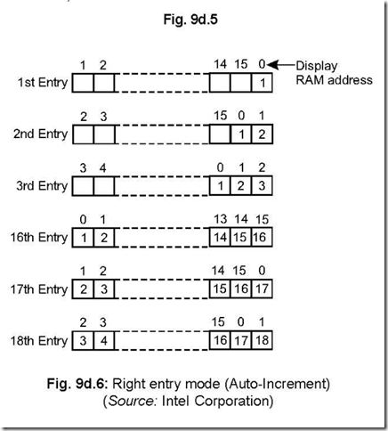
Ans. In the right entry (calculator) mode, the characters are entered from the right most position. As characters are entered one after another, the present data occupies the right most position, just the earlier one occupies the left of the right most position etc. This is explained in Fig. 9d.6.
In this mode, no correspondence exists between RAM address and the display position.
15. What are the different types of software operations possible with 8279. Ans. The following software operations are possible with 8279:
z Keyboard/display mode set
z Program clock
z Read FIFO/Sensor RAM
z Read Display RAM
z Write Display RAM
z Display Write Inhibit/Blanking
z Clear
z End Interrupt/Error Mode Set
z Status Word.
16. In how many ways data can be entered into a microprocessor?
Ans. There are three different ways of entering data into microprocessor—these are
z reading data from a DIP (on/off) switch.
z reading data from push-button keys.
z keys arranged in matrix form and read by software technique.
17. What is meant by contact bounce? How it is eliminated?
Ans. When an electromechanical switch is switched over from an off to on condition, the contact does not become firm on the first count. It loses contact and then makes it—this process repeats itself for a number of times before the contact is firmly placed. This occurs for a very small duration of time.
This thus leads to erroneous operation in digital circuits. This problem can be eliminated by a hardware circuit—called ‘contact debouncers’ or by software technique (by a delayed reading so that the transient period is over) in microprocessor based systems.
