ASSIGNMENTS
1. Explain why the number of output ports in peripheral-mapped I/O is restricted to 256 ports.
2. In peripheral-mapped I/O, can an input port and an output port have the same port address?
3. If an output and input port can have the same 8-bit address, how does the Z80 differentiate between the ports?
4. Specify the two control signals required to latch data in an output port.
5. Specify the type of pulse required to latch data in the 7475.
6. Are data latched in the 7475 at the leading edge, during the level, or at the trailing edge of the enable (E) signal?
7. If the control signals W̅R̅ and I̅O̅R̅Q̅ are asserted at the same time, can data be latched using only the control signal W̅R̅?
8. If the answer to the previous question is yes, what are potential problems with the interfacing circuit?
9. In Figure 5.4, explain why the LED cathodes rather than anodes are connected to the latch.
10. Specify the control signals required to enable an input port.
11. Explain why a latch is used for an output port, but a tri-state buffer can be used for an input port.
12. What are the control signals necessary in memory-mapped I/O?
13. Can the microprocessor differentiate whether it is reading from a memory mapped input port or from memory?
14. In Figure 5.11, connect the output of the comparator to data line D7 and also drive the transistor with bit D7 • Make the necessary changes in the instructions.
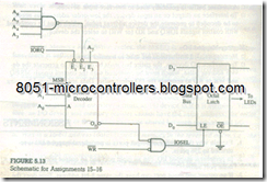
15. Identify the port address in Figure 5.13.
16. In Figure 5.13, if O̅E̅ is connected directly to the W̅R̅ signal and the output of the decoder is connected to the latch enable (through an inverter), can you display a byte at the output port? Explain your answer.
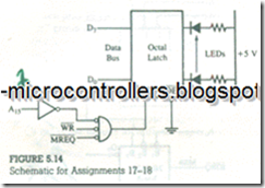
17. In Figure 5.14, determine whether it is the memory-mapped or the peripheral-mapped I/O.
18. In Figure 5.14, what is the port address if all the "don’t care" address lines are assumed to be at logic 0?
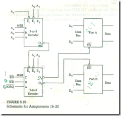
19. In Figure 5.15, are ports A and B input or output ports?
20. In Figure 5.15, what are the addresses of ports A and B?
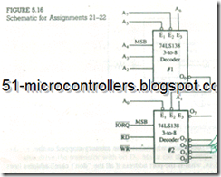
21. In Figure 5.16, identify two output lines of decoder #2 that can be used as control signals and explain their functions. Explain why other output lines cannot be used as control signals.
22. In Figure 5.16, specify the I/O addresses.
23. In Figure 5.17, the decoder 74LS155 and an 8-input NAND gate are used to decode the address bus and generate the control signals. The decoder has two input lines (A1 and A0) and four enable lines (pins 1,2,14, and 15).
When pins 14 and 15 (active low) are enabled, the four output lines of the "b" group decode the input signal, and when pins 1 (active high) and2 (active low) are enabled, the four output lines of the "a" group decode the input signals. Identify the addresses that can assert the output lines of the decoder and specify their I/O functions.
24. Sketch the waveforms of the M1 cycles in the diagnostic routine (section 5.8).
25. Write a similar diagnostic routine to test the circuit in Figure 5.8
26. Is there a W̅R̅ pulse in your diagnostic routine of 25? If the answer is no, what is the unique identifiable signal that can be used to sync the scope?


