5.8 TROUBLESHOOTING I/O INTERFACING CIRCUITS
In the last several sections, we discussed the interfacing of I/O devices and instructions to test them. In I11ustrative Example 1(Figure 5.4), the test program includes two instructions that load the byte 97H into the accumulator and output the byte to port 07H• If we execute these instructions and no change is observed at the output port, we must implement the troubleshooting technique similar to that which we used for troubleshooting memory interfacing circuits in the last chapter. After checking the wiring and the pin connections, we can write a diagnostic routine and execute it in a continuous loop to generate a constant and identifiable signal, and then check various points in relation to that signal.
DIAGNOSTIC ROUTINE AND MACHINE CYCLES
We can use the same instructions for the diagnostic routine that we used in Illustrative Example 1; however, to generate a continuous signal, we need to .add a Jump instruction, as shown.
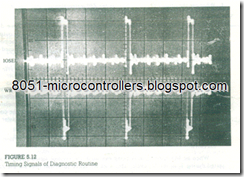
This loop has 28 T-states and eight operations (machine cycles). To execute the loop once, the microprocessor asserts the R̅D̅ signal seven times (the Opcode Fetch is also a Read operation) and the W̅R̅ signal once. Assuming the system clock frequency is 2 MHz, the loop is executed in 14 µS, and the WR signal, repeated every 14µS, can be observed on a scope. If we sync the scope on the W̅R̅ pulse from the Z80, we can check the output of the 8-input NAND gate (I̅O̅A̅D̅R̅), I̅O̅W̅R̅, and I̅O̅S̅E̅L̅ signals; W̅R̅ and I̅O̅S̅E̅L̅ signals of a working circuit are shown in Figure 5.12.
When the Z80 asserts the W̅R̅ signal, the port address 07H must be on the address bus A7-Ao, and the output of the NAND gate must be low. Similarly, the I̅O̅W̅R̅ must be low, and the IOSEL must be high. Now if we check the data bus in relation to the WR signal, one line at a time, we must read the data byte 97H.

