In this section, we will illustrate memory interfacing with the Z80 microprocessor by using an actual chip: the 2764 PROM (Erasable Programmable Read-Only- memory). This is a memory chip commonly used in industry to develop microprocessor-based products .. In this illustration, we will assume that the chip bas been already programmed-that is the binary patterns representing Z80 instructions are stored in it-and we will only read from it , we focus only on the interfacing concepts, Interfacing logic circuit, and memory addresses.
2764 EPROM
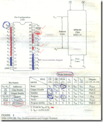
This is an 8K (8192 x 8) memory chip with eight data lines and is housed in a 28-pin package : Figure 6 shows the logic pinout and the pin configuration. It has thirteen address lines, A12-A0 to identify 8192 registers one chip select signal shown as chip enable (C͞E) and one output Enable (O͞E) signal to enable the output buffer.
FIGURE 6
2764 EPROM: Pin Configuration and Logic Symbol
It operates from a single + 5 V power supply in the Read mode and requires +21 V pulse Vpp to program It . the pinout of this memory chip is compatible with 27128 ( 16K x 8) and 2256 (32K x 8) EPROMs; thus, the memory size can be expanded to 16K or 32K by merely replacing the chip. The chip has a quartz window, and the information stored in this memory can be erased by ex posing the window to ultraviolet light for 15 to 20 minutes. The erasing process sets all the bits to logic 1. To avoid accidental erasures from direct sunlight or fluorescent lights, the window should be covered with an opaque label. Once it is erased, the chip can be used again to store a new program. The programming is done by using a circuit called an EPROM programmer that can selectively store logic 0 in bit positions In memory registers by providing a 21 V pulse to Vpp
Interfacing Circuit
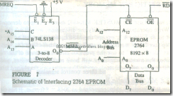
Figure 7 shows a complete schematic of interfacing the 2764 with the Z80 microprocessor. We will describe this circuit in terms of the four steps required for interfacing, as listed in the previous section.
Step 1 : Connect the necessary address lines to the memory chip.
Figure 7 shows that the address lines A12-A0 are connected to the memory
chip to identify 8192 registers.
Step 2 Decode the remaining address lines and combine the M͞R͞E͞Q with the & decoded pulse to generate the Memory Select (M͞S͞E͞L) pulse.
Step 3:
In this schematic, two steps-the decoding of the address and generating the Memory Select (M͞S͞E͞L)-are combined by using the 74LS138 3-to-8 decoder. The decoder has three inputs, three enable lines, and eight output lines. Two enable lines are active low, and one is active high. Once the decoder is enabled, only one output line, corresponding to the input, combination, goes active (low).
FIGURE 7
Schematic of Interfacing 2764 EPROM
In Figure 7, the output O0 of the decoder is shown as Memory Select (M͞S͞E͞L0), which is connected to the Chip Enable (C͞E) of the memory, and O0 goes active low when the address lines A15– A13 the M͞R͞E͞Q are all at logic 0 . The control signal M͞R͞E͞Q is used to enable the decoder (active low); the address lines A15, A14, and A13 are used as input to the decoder; the enable line E3 is connected to + 5 V; and E2 is grounded. No other logic level on these address lines can assert the M͞S͞EL0 signal.
Step 4: Connect the Z80 control signal to enable an appropriate buffer.
Figure 7 shows that the Z80 Read (R͞D) is connected to the R͞D signal of the memory chip. When the R͞D signal is asserted, the output buffer is enabled and the data byte from the selected register is placed on the data bus.
Memory Map
We can obtain the address range of this memory chip by analyzing the possible logic levels on the 16 address lines. The logic levels on the address lines A15-AI3 have to be 0 to assert the Chip Enable, and the address lines A12-A0 can assume any combinations from all 0s to all 1s. Therefore, the memory map (the address range) of this chip is from 0000H to 1FFFH as shown below.
We can verify the memory map in terms of our analogy of page and line numbers. The chip has 8192 bytes of memory that can be viewed as 32 pages with 256 lines each. Let us examine the high-order Hex digits of the map; they range from 00 to 1F indicating 32 pages-0000 to 00FF, 0100 to 01FF, for example.

