DIGITAL LOGIC ELEMENTS
Digital logic elements are the basic circuits that are used to process the binary data. The logic element has one or more binary data inputs to be processed. The logic element processes or manipulates the binary input signals in a fixed way and generates an appropriate output signal. The output is a function of the binary states of the inputs and the unique processing capability of the logic element. The logic element “looks” at the binary input signals, and then makes a decision and generates an appropriate output. There are five elementary logic circuits: inverter or NOT, AND, OR, NAND, and NOR. These functions are performed by logic elements known as inverters and gates.
You need not be concerned with the inner workings of these logic elements. Instead, your primary concern is with the basic logic functions. Needless to say, the gates and inverters are inside every microcomputer and digital integrated circuit.
Inverter
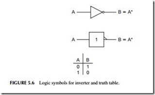
The inverter has a single input and a single output. The logic function per- formed by an inverter is inversion. The output of the inverter is simply the inverse, or opposite, of the input. Because binary signals can assume only one of two different states, either 0 or 1, the inverter generates a 0 when the input is a 1, and a 1 when the input is a 0.
Two common symbols used to represent an inverter are shown in Figure 5.6. The input and output are given names, which are usually letters of the alphabet.
There are a variety of ways to express the operation of various logic functions. One way is to use Boolean algebraic expressions. A Boolean expression is a simple mathematical or algebraic formula that expresses the output in terms of the input. The Boolean expression for the inverter is:
This equation is read, “B equals not A.” The asterisk means NOT or inversion. What this expression is telling you is that if the input is A, the output, B, is not A.
Another method of expressing the function of a logic element is a truth table. This is simply a table listing all possible combinations of the inputs and outputs of a logic element. Figure 5.6 also shows the truth table for an inverter. There are only two possible inputs, 0 and 1, and the corresponding outputs. A truth table completely defines the operation of a logic element.
AND Gate
A gate is a circuit that has two or more inputs and a single output. The gate generates a binary output that is a function of the states of the inputs and the nature of the gate itself.
The type of gate determines how the binary inputs are processed. The two basic logic gates are the AND gate and the OR gate. An AND gate is a logic circuit that generates a binary 1 output if all of its inputs are binary 1’s. Otherwise, the circuit generates a binary 0. All of the inputs have to be binary 1 for the AND gated to produce a binary 1 output. If any one of the inputs is a binary 0, the output is binary 0.
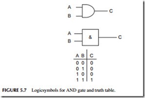
Figure 5.7 shows the logic symbols used to represent an AND gate. Letters of the alphabet are used to represent inputs and outputs. There may be more than two inputs, but there is only one output.
As with the inverter, the output of the AND gate can be expressed in terms of the inputs with a Boolean expression. The Boolean expression for an AND gate is:
C = AB
This equation is read, “C equals A and B. ”Parentheses also can be used to separate the inputs; for example, C = (A)(B).
The truth table for a simple two-input AND gate is also shown in Figure 5.7. Note that the output C is a binary 1 when both inputs are binary 1’s. At all other times, the output is binary 0. With two inputs, there are a total of four different input combinations (22 = 4). With three inputs, there are 23 = 8 possible input combinations for an AND gate. These inputs are the binary numbers 000 through 111.
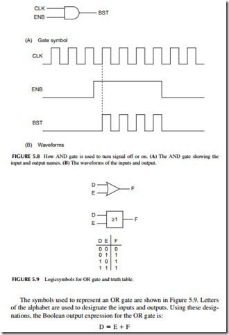
One of the most common applications of an AND gate in digital circuits is gating. Gating simply refers to the use of one binary signal to control another. A two-input AND gate is most often used as a control gate. One input signal is the control that either keeps the other input signal from passing through to the output or allows it to pass.
Figure 5.8 shows the inputs and output of a typical control gate. Note that multiletter names called mnemonics are used instead of single letters to designate the input and output signals. The ENB or enable input represents the control signal. As long as the ENB input is a binary 0, the output is a binary 0. The gate is said to be inhibited because nothing more than a binary 0 output occurs.
When the ENB control input is a binary 1, the gate is enabled. At this time, the main input signal, CLK for clock, is allowed to pass through to the out- put BST. CLK is a periodic clock signal that switches repetitively between the binary 0 and the binary 1 levels at a fixed frequency. The output of the AND gate follows the CLK input as long as the ENB control input is a binary 1.
OR Gate
Another commonly used logic gate is the OR circuit. Like the AND gate, the OR gate has two or more inputs and a single output. The OR gate generates a binary 1 if any one or more of its inputs are binary 1. The only time the output of an OR gate is binary 0 is when all its inputs are binary 0.
This equation is read, “D equals E or F.” In this Boolean expression, the plus sign designates the OR function. In a Boolean logic expression, the plus sign does not mean addition. In Figure 5.9, the mathematical symbol> (greater than or equal to) is used to designate the OR logic function. The truth table for an OR gate further defines its operation. The output D is a binary 1 when input E or input F or both are a binary 1. Like an AND gate, an OR gate can have any number of inputs.
NAND and NOR Gates
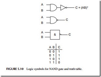
The AND and OR logical functions are basic to all digital systems. Although these functions are implemented with AND and OR gates, a variation of these gates is even more widely used. These are NAND and NOR gates, which are a combination of either an AND gate or an OR gate and an inverter. These gates are more flexible in their application when they are used together.
A NAND gate can be made with an AND gate followed by an inverter. Figure 5.10 shows this circuit configuration. Note the two special symbols in Figure 5.10 used to represent the logical NAND function. The truth table is also given.
A NAND gate can perform all of the gating and detection functions mentioned earlier for an AND gate. The only difference is that the output is inverted.
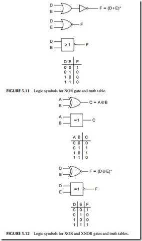
The other widely used digital logic element is a NOR gate. A NOR gate is a combination of an OR gate followed by an inverter (see Figure 5.11 ). The symbols used to represent the NOR logic function are also shown. The out- put of a NOR gate is simply the complement of the output of an OR gate, as shown by the truth table. An XOR actually is a 1-bit binary adder.
Exclusive OR Gate
A variation of the OR gate is the exclusive OR, usually designated XOR. Its symbols are given in Figure 5.12. The truth table is also shown. Note that the
circuit only produces a 1 output if the two inputs are opposite. The output is 0 if the two inputs are the same.
An inverted XOR or XNOR has the symbols and truth table shown in Figure 5.12. It is useful as a 1-bit comparator since the output is 1 if both inputs are the same.
Flip-Flops
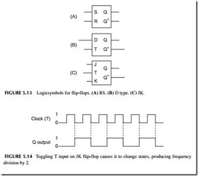
A flip-flop (FF) is another basic building block of electronics. It is essentially a circuit that stores 1 bit of data. The circuit has two states—set and reset. If the FF is storing a binary 1, it is set. If it is storing a binary 0, it is reset. Figure 5.13A shows the basic block diagram of a reset-set (R-S) FF. The inputs are set (S) and reset (R). The two outputs Q and Q* are complementary. You apply an input to the appropriate input to set or reset the FF.
A D-type flip-flop is shown in Figure 5.13B. It has a D or data input and a clock (T) input. When the clock occurs, the FF is either set or reset depending on the value of the D input. The D FF is used to store 1 bit of data.
Another type of FF is the JK, shown in Figure 5.13C. It has J and K inputs that correspond to S and R inputs, respectively. It also has a clock or T input that performs the set or reset operations. To store a binary 1, you make J = 1 and K = 0. When a clock input occurs, the FF is then set or reset.
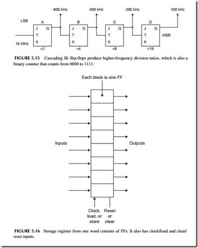
The T input also causes the state of the FF to toggle or change state when a clock transition occurs (see Figure 5.14 ). This feature is used to produce frequency division by 2 as shown. The output is a square-wave half the frequency of the T input. Additional JK FFs can be cascaded to produce frequency division by the power of 2 or 2, 4, 8, 16, 32, 64, and so on, as shown in Figure 5.15.
Storage Registers
A storage register is a place to store a binary word or number. It is made up of 1 FF per bit. An 8-bit register stores bytes and has 8 FFs. Figure 5.16 shows a register with eight inputs and eight outputs. Most registers also have a clock input also called LOAD or STORE that determines when the input data is stored. Some also have a CLEAR or RESET input that puts all the FFs in the binary 0 state.
Shift Registers
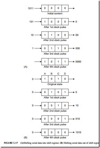
A shift register (SR) is like a storage register, but the bits stored there may be shifted from one FF to the next as each clock pulse occurs. Figure 5.17A shows how serial binary data is shifted into the SR for storage. As new data
is shifted in, the existing data will be shifted out and sent to another circuit. Figure 5.17B shows data being shifted out as binary 0’s are shifted in.
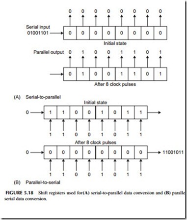
Shift registers are often used for parallel-to-serial and serial-to-parallel conversions. A serial-to-parallel conversion is shown in Figure 5.18A. The SR initially contains all binary 0’s. Then serial data is shifted in and the output is taken in parallel from the FF outputs. For parallel-to-serial conversion, a binary word is initially stored in the register. Then the word is shifted out as the clock pulses occur (see Figure 5.18B).
Counters
As its name implies, a counter is a circuit that counts input pulses. Counters are made of multiple cascaded FFs, and they are sometimes accompanied by logic gates. As the input pulses occur, the binary number stored in the counter FFs tells how many pulses have occurred. The frequency divider shown in Figure 5.15 is also a 4-bit counter. It can count from 0 (0000) to 15 (1111).
If all FFs are initially reset to 0, then 10 pulses occur, and the FFs from A to D would be storing 0101 from left to right. The right-most FF (D) is the MSB, so you read the counter as 1010 or the binary equivalent of decimal 10.
Binary counters can store numbers up to 2N – 1, where N is the number of FFs. For example, an 8-bit counter would count from 00000000 to 11111111 or 28 – 1 = 256 – 1 = 255.
Figure 5.19 shows a counter where 178 pulses have occurred, so the counter stores the number 10101011 that is the binary equivalent of 179.
Another popular form of counter is the BCD version that counts from 0000 to 1001 or 0 through 9. BCD counters are used to keep track of decimal quantities in binary form. BCD counters can serve as frequency dividers as well. Each divides by 10.
Related posts:
Incoming search terms:
- basic logic elements
- what are the basic logic elements
- 4 and logic elements
- what are the basic logic elemnts
- https://yandex ru/clck/jsredir?from=yandex ru;search;web;;&text=&etext=1834 c4-wm9cv0rmbeCOSX7BT9u8ONs_BKv3qp_Uitr75BoFuQ64oia8JhTxBZ_R7bgTFszUpynVDvjDUf8V5CmOMYg beb3c71b044e0b31ca5c684176c550b039a1a7f6&uuid=&state=_BLhILn4SxNIvvL0W45KSic
- electronic logic element
- Digital logic element
- Characteristics of an ideal digital logic element
- basiclogic element s
- what are the basic logic eliment
