DATA TRANSMISSION I/O DEVICES
Within a microprocessor chip, digital signals travel from one component to another through an integrated circuit termed a data bus. One part of the bus runs between the prime (system or main) memory and microprocessor, and another connects the prime memory to various storage and peripheral devices. The segment of the data bus that extends between the prime memory and peripheral devices is called the extension bus, or I/O bus in most cases. As signals move along the I/O bus, they can travel through expansion slots, cards, ports and connectors to peripheral devices.
An I/O port can only host one client; in contrast, an I/O bus can serve several. This section will introduce these I/O buses, including PCI (peripheral component interconnect), ISA (industry standard architecture), USB (universal serial bus), Firewire or IEEE-1394, and IEEE-488. The transmission ports discussed include AGP (accelerated graphics port), parallel ports, IDE (integrated drive electronics) ports, and SCSI (small computer system interface) ports.
The RS (recommended standards) series mainly include RS-232, RS-422, RS-485, and RS-530. They are used as the connectors connecting DTEs such as computers and programmable controllers with DCEs such as modems. The RS series are standard interfaces between a computer and some special peripherals such as modems, mouse, and keyboard, etc.
14.2.1 I/O buses
(1) PCI (peripheral component interconnect) bus Intel has developed a standard interface, named the PCI local bus, for microprocessor chips. This technology allows fast memory, disk and video access. It is now the main interface bus used in most programmable controllers, and is rapidly replacing the ISA bus for internal interface devices. It is very adaptable, and most external buses, such as SCSI and USB, connect to the microprocessor by using it.
The PCI local bus has two variants: conventional PCI and the PCI-X bus. PCI-X is a high- performance variant of 64-bit PCI designed for servers. PCI-X adapters and slots are backward- compatible with 32-bit PCI slots and adapters.
The PCI bus transfers data using the system clock and can operate over a 32-bit or 64-bit data path. If data are transferred at 64 bits at a rate of 33 MHz, then the maximum transfer rate is 264 Mbps. The 32-bit or 64-bit memory address space can reach 4 gigabytes or 16 exabytes, respectively. Each device slot of a PCI local bus can have a configuration space up to 256 bytes. The PCI-X specification also provides options for 3.3 V signalling, 64-bit bus width, and 66 MHz clocking on server motherboards.
The PCI operations, including the bus transaction, bus arbitration, bus configuration, and PCI bus interrupt handling are given briefly in the following.
(1) PCI bus transactions
Each PCI bus transaction is made up of an address phase followed by one or more data phases. Any PCI bus device (or client) may initiate a bus transaction. First, this device must request permission from a PCI bus arbiter on the microprocessor chip. The arbiter grants permission to one of the requesting devices, which then becomes the bus master or initiator. The bus master begins the address phase by broadcasting a 32-bit address plus a 4-bit command code, and then waits for a target to respond. All other devices examine this address and one of them responds a few cycles later.
The direction of the data phases may be from initiator to target (write transaction) or vice versa (read transaction), but all of the data phases must be in the same direction. Either party may pause or halt the data phases at any point. While the PCI bus transfers 32 bits per data phase, the initiator transmits a 4-bit byte mask indicating which 8-bit bytes are to be considered significant. In particular, a masked write must affect only the desired bytes in the target PCI device.
The commands that refer to cache lines depend on the PCI configuration space cache line size register being set up properly; they may not be used until that has been done. There are 16 possible 4-bit command codes, and 12 of them are assigned. With the exception of the unique dual address cycle, the least significant bit of the command code indicates whether the following data phases are a read (data sent from target to initiator) or a write (data sent from an initiator to target). PCI targets must examine the command code as well as the address and not respond to address phases which specify an unsupported command code.
(2) PCI bus arbitrations
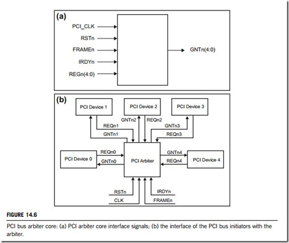
The PCI bus arbiter is used to efficiently manage the accesses to a PCI bus that is shared by several masters. Access to the PCI bus is automatically determined by the individual priorities of each master. At any given time, more than one PCI bus initiator may request use of the PCI bus by asserting its specific request signal (REQn). The arbiter determines which PCI bus initiator controls the PCI bus, by asserting that device’s specific grant signal (GNTn). Figure 14.6(a) shows the PCI arbiter interface signals and Figure 14.6(b) illustrates the relationship of the PCI bus initiator device with the bus arbiter.
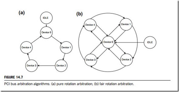
The arbiter can use two algorithms to resolve any conflicts due to multiple requests. The first is “pure rotation”, which is a turn-based method that allows each bus master one transaction in turn. If only one master requests the bus, that master will immediately get the grant. Figure 14.7(a) illustrates the pure rotation scheme.
“Fair rotation” is the second algorithm which is employed if an embedded microprocessor is required to initialize the system, but will not be used after that point. By giving it highest priority, the fair rotation scheme allows the embedded processor access to the PCI bus on every other transaction when it is requesting the bus continuously. The other masters use a pure rotation scheme. The fair rotation scheme is illustrated in Figure 14.7(b).
(3) PCI bus configurations
As mentioned, each PCI bus device can have a block of 256 bytes of configuration space: 16 doublewords (each double word consists of 32 bits) are taken as header information plus 48 doublewords of device-specific configuration registers. The header contains a vendor ID and device type, flags which show whether the device generates interrupts, whether the device is 66 MHz-capable and other low-level performance-related information. It also contains the base address locations of I/O ports, RAM and expansion ROM, the maximum latency register (mentioned in subsection 5.1.1) and
other similar general information. ROMs can contain code for different microprocessor architectures, and a configuration register shows which ones are supported.
In a typical system, the firmware (nucleus or kernel of the operating system) queries all PCI buses at start-up time via the PCI configuration space to find out what devices are present and what system resources (such as memory space, I/O space, interrupt lines, etc.) each needs. It then allocates the resources and tells each device what its allocation is. The PCI configuration space also contains a small amount of device type information, which helps an operating system to choose device drivers for it, or at least to have a dialogue with a user about the system configuration. These are typically necessary for devices used during system start-up, before device drivers are loaded by the operating system.
(4) PCI bus interrupts
The PCI bus includes four interrupt lines (INTA#, INTB#, INTC#, and INTD#), all of which are available to each device. However, they are not wired in parallel like the other PCI bus lines.
The positions of the interrupt lines rotate between slots, so what appears to one device as the INTA# line is INTB# to the next and INTC# to the one after that. Single-function devices use their INTA# for interrupt signaling, so the device load is spread fairly evenly across the four available interrupt lines. This alleviates a common problem with sharing interrupts.
PCI bridges (between two PCI buses) map the four interrupt traces on each of their sides in varying ways. Some use a fixed mapping, and in others it is configurable. Software generally cannot determine which interrupt line a device’s INTA# pin is connected to across a bridge. The mapping of PCI interrupt lines onto system interrupt lines, through the PCI host bridge, is similarly implementation- dependent. The result is that it can be impossible to determine how a PCI device’s interrupts will appear to software. Platform-specific BIOS (basic input/output system) code is meant to know this, and to set a field in each device’s configuration space indicating which the interrupt request signal, IRQ, is connected to, but this process is not reliable.
Later revisions of the PCI specification add support for message-signalled interrupts. In this system a device signals its need for service by performing a memory write, rather than by asserting a dedicated line. This alleviates the problem of scarcity of interrupt lines, and even if interrupt vectors are still shared, it does not suffer the sharing problems of level-triggered interrupts. It also resolves the routing problem, because the memory write is not unpredictably modified between device and host. Finally, because the message signaling is in-band, it resolves some synchronization problems that can occur with posted writes and out-of-band interrupt lines.
(2) ISA (industry standard architecture) bus IBM developed the Industry Standard Architecture or ISA bus for their 80286-based AT (advanced technology) computer (IBM AT). Apart from specialized industrial use, ISA bus is all but gone today. Even where present, system manufacturers often shield customers from the term “ISA bus”, referring to it instead as the “legacy bus”. In practice there is no speed difference between running many serial communication peripherals using a PCI or an ISA bus, though the PCI advantage is obvious for high-speed devices such as video cards. Thus, there is no reason to convert an ISA serial communication system to PCI bus, as ISA will provide equivalent functionality, generally at a lower price.
Initially the ISA bus had the advantage of being able to deal with 16 bits of data at a time. An extra edge connector was added to give compatibility with a PC/AT bus. This gives an extra eight additional data lines for a total of 16 bits, and four address lines for a total of 24 bits. Thus, the ISA bus has a 32- bit data and a 24-bit address bus. It also adds new interrupt lines connected to a second 8259 PIC (programmable interrupt controller) connected to one of the lines of the first and four 16-bit DMA (direct memory access) channels, as well as control lines to select 8- or 16-bit transfers.
The PC/AT bus was designed with an expansion bus which not only took advantage of the new technology, but also remained compatible with the older-style 8-bit PC/XT add-in boards. Anticipating that advances in microprocessors would again outpace advances in bus technology, the PC/AT bus had two separate oscillators. In this way, the microprocessor and expansion bus could be run on different clocks with different speeds. Therefore, a controller or computer running a newer processor with 33 MHz clock speed could also run its expansion bus at an 8 MHz clock rate. ISA cards are more cumbersome to install than other cards because I/O addresses, interrupts, and clock speed must be set using jumpers and switches on the card itself. Other bus options, which use software to set these parameters, are called plug-and-play. While there is nothing inferior about using jumpers and switches, it can be more intimidating for novice users. The ISA system, however, does not have a central registry from which to allocate system resources. Consequently, each device behaves as though it has sole access to system resources such as DMA, I/O ports, IRQs, and memory. Obviously, this can cause problems when using multiple add-in boards in a single system.
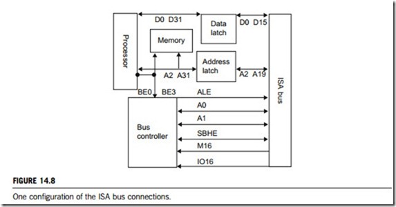
Figure 14.8 shows a typical connection to the ISA bus. The ALE (sometimes known as BALE) controls the address latch; when active low, it latches the address lines A2 A19 to the ISA bus. The address is latched when ALE goes from a high to a low. The Pentium’s data bus is 64 bits wide,
whereas the ISA expansion bus is 16 bits wide. It is the bus controller’s function to steer data between the microprocessor and the slave device for either 8-bit or 16-bit communications.
(3) USB (universal serial bus) bus
The USB (universal serial bus) is mainly used for communication between a computer and peripheral devices, replacing many varieties of serial and parallel ports for the connection of medium-bandwidth peripherals such as keyboards, scanner, modem, video, game or graphic controller, music interface, etc. The great advantage of USB is that it allows for peripherals to be added and deleted from the system without causing any upsets. The system will also automatically sense the connected device and load the required driver.
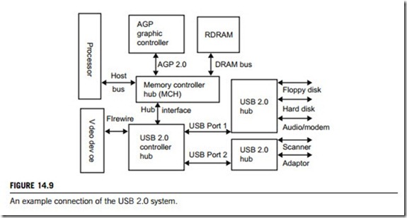
USB is a balanced bus architecture that hides the complexity of the operation from the devices connected to it. The USB host controller controls system bandwidth. Each device is assigned a default address when first powered or reset, and hubs and functions are assigned a unique device address. All USB devices are attached to the USB via a port. Hubs indicate the attachment or removal of a USB device in its port status. Figure 14.9 shows an example of the USB 2.0 system, where a memory hub is used to provide a fast data transfer, while the Firewire connection provides ultrahigh-speed connection for video transfers. The USB connection provides low-high and full- speed connections to most of the peripherals that connect to the system. Such connections can be internal or can connect to an external hub. There are two main methods to implement USB, as given below.
1. Open host controller interface (OHCI). This method defines the register-level interface that enables the USB controller to communicate with the host computer and the operating system. OHCI is an industrial standard hardware interface for operating systems, device drivers, and the BIOS to manage the USB. It optimizes performance of the USB bus while minimizing CPU overhead by using scatter/gather bushmaster hardware support. It has efficient isochronous data transfers allowing for high USB bandwidth without slowing down the host CPU, and ensures full compatibility with all USB devices.
2. Universal host controller interface (UHCI). This method defines how the USB controller talks to the host computer and its operating system. It is optimized to minimize host computer design complexity and uses the host CPU to control the USB bus. This method has the advantage of simple design, which reduces the transistor count required to implement it, thus reducing the system cost. Furthermore, it can provide full compatibility with all USB devices.
In data transmission, UHCI supports two types of transfers: stream and message. A stream has no defined structure, whereas a message does. At start-up, one message pipe, control pipe 0, always exists as it provides access to the device’s configuration, status, and control information. USB optimizes large data transfers and real-time data transfers. When a pipe is established for an endpoint, most of its transfer characteristics are determined, and remain fixed for its lifetime. Each bus transaction involves the transmission of up to three packets, which can be (1) token packet transmission, (2) data packet transmission, and (3) handshake packet transmission. With these transfer characteristics, USB defines the following four transfer types:
(i) Control transfers. This is bursty, aperiodic, host-software-initiated request/response communication typically used for command/status operations.
(ii) Isochronous transfers. This is periodic, continuous communication between host and device typically used for time-relevant information. This transfer type also preserves the concept of time encapsulated in the data. This does not imply, however, that the delivery needs of such data are always time-critical.
(iii) Interrupt transfers. This is small data, aperiodic, low-frequency, bounded latency, device-initiated
communication typically used to notify the host of device service needs.
(iv) Bulk transfers. Aperiodic, large, bursty communication typically used for data that can use any available bandwidth and also is delayed until bandwidth is available.
As mentioned earlier, a major advantage of USB is the hot attachment and detachment of devices. USB does this by sensing when a device is attached or detached. When this happens, the host system is notified, and system software interrogates the device, determines its capabilities, and automatically configures it. All the required drivers are then loaded and applications can immediately make use of the connected device.
(a) Attachment of USB devices
All USB devices are addressed using the USB default address when initially connected or after they have been reset. The host determines whether the device is a hub or a function and assigns it a unique USB address. The host then establishes a control pipe using assigned USB address and endpoint number zero. If the device is a hub and USB devices are attached to its ports, then the above procedure is followed for each of the attached devices. If the attached USB device is a function, then attachment notifications will be dispatched by USB software to interested host software.
(b) Removal of USB devices
When a USB device has been removed from one of its ports, the hub automatically disables the port and provides an indication of device removal to the host. If the removed USB device is a hub, then the removal process must be performed for all of the USB devices previously attached to it. If the removed USB device is a function, removal notifications are sent to interested host software.
(4) Firewire or IEEE-1394 Bus
The main competitor to USB is the Firewire standard (IEEE 1394 1995 buses), which is a high- speed serial bus typically used for video transfers, whereas USB supports a low-to-medium-speed serial bus for a greater range of peripherals. Firewire supports rates of approximately 100, 200, and 400 Mbps, known as S100, S200, and S400, respectively. The future standard promises higher data rates, and ultimately it is envisaged that rates of 3.2 Gbps will be achieved, when optical fiber is introduced into the system. It uses point-to-point interconnect with a tree topology: 1000 buses with 64 nodes gives 64,000 nodes. Firewire can also have automatic configuration and hot plugging, and can perform both asynchronous and isochronous data transfer, where a fixed bandwidth is dedicated to a particular peripheral. This should subsequently reduce the costs of production of controller interfaces and peripheral connectors, as well as simplifying the requirements placed on users when setting up their devices. Firewire is therefore a more economical interface bus standard that performs fast and high-bandwidth data transmissions but it does have a maximum cable length of 4.5 meters.
There are two bus categories in Firewire:
(a) Cable. This is a bus that connects external devices via a cable. This cable environment is an acyclic network with finite branches consisting of bus bridges and nodes (cable devices). Acyclic networks contain no loops and result in a tree topology, with devices daisy-chained and branched (where more than one device branch is connected to a device). Devices on the bus are identified by node IDs. Configuration of the node IDs is performed by the self ID and tree ID processes after every bus reset. This happens every time a device is added to or removed from the bus, and is invisible to the user.
(b) Backplane. This type of topology is an internal bus. An internal IEEE-1394 device can be used alone, or incorporated into another backplane bus. Implementation of the backplane specification lags behind the development of the cable environment, but one could imagine internal IEEE- 1394 hard disks in one computer being directly accessed by another IEEE-1394 connected computer.
One of the key capabilities of IEEE-1394 is isochronous data transfer, although both asynchronous and isochronous are supported, and are useful for different applications. Isochronous transmission transfers data such as real-time speech and video, both of which must be delivered uninterrupted, and at the rate expected, whereas asynchronous transmission is used to transfer data that are not tied to a specific transfer time. With IEEE-1394, asynchronous transmission is generally used to send data to an explicit address, and get confirmation when it is received. Isochronous transfer, however, is an unacknowl- edged guaranteed bandwidth transmission method, useful for just-in-time delivery of multimedia-type data.
An isochronous “talker” requests an amount of bandwidth and a channel number. Once the bandwidth has been allocated, it can transmit data preceded by a channel ID. The isochronous listeners can then listen for the specified channel ID and accept the data following it. If the data are not intended for a node, it will not be set to listen on the specific channel ID. Up to 64 isochronous channels are available, and these must be allocated, along with their respective bandwidths, by an isochronous resource manager on the bus.
By comparison, asynchronous transfers are sent to explicit addresses on the IEEE-1394 bus. When data are to be sent, they are preceded by a destination address, which each node checks, to identify packets for itself. If a node finds a packet addressed to itself, it copies it into its receive buffer. Each node is identified by a 16-bit ID, containing the 10-bit bus ID and 6-bit node or physical ID. The actual packet addressing, however, is 64 bits wide, providing a further 48 bits for addressing a specific offset within a node’s memory.
(5) IEEE-488 bus
The IEEE 488 is a common parallel interface standard, originally developed by the Hewlett-Packard Corporation in 1974, and called the HP-IB (Hewlett-Packard interface bus). This interface bus became so popular that it was adopted by the IEEE (Institute of Electrical and Electronics Engineers) in 1975 and designated the IEEE-488 standard. In common practice, IEEE-488 is referred to as the GPIB interface (general purpose interface bus), so IEEE-488, GPIB, and HP-IB all refer to the same parallel interface standard.
The primary purpose of the GPIB is to interface laboratory instruments with each other, and with computers. Both devices must have a GPIB interface card installed, and the computer must be running a GPIB controller program for the connection to operate.
Almost any instrument can be used with the IEEE-488 specification, because it is indepentdent of the function of the instrument itself, or about the form of the instrument’s data. Instead, the specifi- cation defines a separate component, the interface, which can be added to the instrument. The signals passing into the interface from the IEEE-488 bus and from the instrument are defined in the standard. The instrument does not have complete control over the interface. Often the bus controller tells the interface what to do. The active controller performs the bus control functions for all the bus instruments.
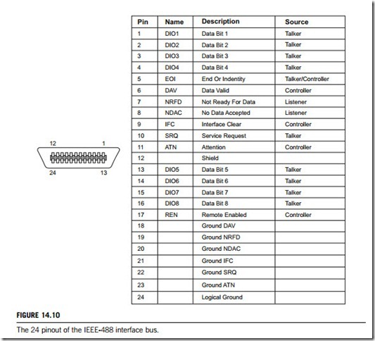
There are 24 lines in the GPIB interface bus and cable (Figure 4.10). Eight of these lines carry data, five are for device control, three are handshaking lines, and eight are signal grounds. IEEE-488 standards give two main types: IEEE-488.1 and IEEE-488.2.
1. The IEEE-488.1 standard greatly simplifies the interconnection of programmable instruments by clearly defining mechanical, hardware, and electrical protocol specifications. For the first time, instruments from different manufacturers were connected by a standard cable. This standard does not address data formats, status reporting, message exchange protocol, common configuration commands, or device-specific commands.
2. The IEEE-488.2 standard enhances and strengthens IEEE-488.1 by specifying data formats, status reporting, error handling, controller functionality, and common instrument commands. It focuses mainly on software protocol issues and thus maintains compatibility with the hardware-oriented IEEE- 488.1 standard. IEEE-488.2 systems tend to be more compatible and reliable.
(1) AGP (accelerated graphics port) port
As computers became increasingly graphically oriented, successive generations of graphics adapters began to push the limits of PCI bus bandwidth. This led to the development of new bus architectures dedicated to graphics adapters. The accelerated graphic port (AGP) is a major advance in the connection of three-dimensional graphics applications, and is based on an enhancement of the PCI bus.
The primary advantage of AGP over PCI is that it provides a dedicated pathway between the slot and the microprocessor, rather than sharing the PCI bus, resulting in faster transfer between the main system memory and the local graphic card, so reducing the need for large areas of memory on the graphics card.
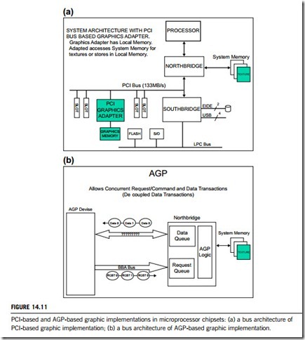
To understand the advantages of AGP graphic implementation, it is necessary to understand the issues that AGP technology has resolved. Figure 14.11(a) shows an architectural diagram of a generic PCI bus-based graphics subsystem. In this architecture, the graphics subsystem resides on the PCI bus. Note that the PCI bus graphics adapter embeds its own local memory on the adapter card. This architecture raises several issues that motivated the need for AGP. Since graphics data such as textures
are stored in main system memory, the PCI bus-based graphics card must access this via the PCI bus. These accesses can occur frequently, particularly if the graphics adapter has a small amount of local memory. Unfortunately, the graphics card must compete with other PCI bus peripherals for bandwidth which may starve other peripherals if these accesses are frequent.
Figures 14.11(b) illustrates how AGP technology elegantly resolves these issues. The system controller embeds the AGP graphic interface, which then uses the PCI bus protocol in tandem with a sideband addressing (SBA) bus for concurrent posting of commands from the graphics card. The Northbridge embeds read and write and command queues (buffers) to allow full-speed data and command transport between the AGP device and the system controller, and concurrent full-speed data transport between the system controller and the system memory.
In summary, the native architecture of the AGP graphics subsystem offers significant raw performance improvement over PCI bus-based graphics subsystems, allowing the graphics subsystem to view and use main memory just like its own local memory meaning the AGP graphics card shares system memory. The card cannot distinguish between system and local memory; it all appears to be local. To the end-user, graphics performance can be enhanced by increasing system memory, rather than by adding expensive graphics memory.
The graphics subsystem no longer needs to compete for PCI bus bandwidth in order to access data in system memory, which allows it to run at full speed with minimal interruption from other components in the system. It also increases system concurrency meaning that the processor, AGP graphics subsystem, and PCI bus device can run independently and concurrently, thus increasing system performance.
There are several modes (data transfer rates) that have evolved over time. The first version is the original AGP-1X mode, offering a data transfer rate of up to 264 Mbps. Second is AGP-2X mode, doubling the data transfer rate to up to 528 Mbps. The third is AGP-4X, offering a transfer rate of up to 1 Gbps. Finally, the fourth version, AGP-8X, offers the highest performance data transfer rate of up to 2.1 Gbps.
(2) Parallel ports
A parallel port is a type of interface found on computers (personal and otherwise) for connecting various peripherals. The IEEE-1284 standard defines the bidirectional version of the parallel port. In its standard form, it allows only for simple communications from the PC outwards. However, like the RS-232, the parallel port is a standard port of the PC.
All parallel ports use a bidirectional link in either a compatible, nibble, or byte mode. These modes are relatively slow, as the software must monitor the handshaking lines (up to 100 kbps). To allow high speeds, the enhanced parallel port and extended capabilities port protocol modes allow high-speed data transfer using automatic hardware handshaking.
(3) IDE (integrated drive electronics) ports
The most popular interface for hard disk drives is the integrated drive electronics (IDE) interface. Its main advantage is that the controller is built into the disk drive, and the interface to the motherboard consists simply of a stripped-down version of the ISA (industry standard architecture) bus. The most common standard is the ANSI-defined ATA-IDE standard. It uses a 40-way ribbon cable to connect to 40-pin header connectors. The standard allows for the connection of two disk drives in a daisy-chain configuration, which can cause problems because both drives have controllers within them. The primary drive is assigned as the master, and the secondary driver is the slave, set by setting jumpers on the disk drive. They can also be set by software that uses the cable select pin on the interface. The specifications for the IDE include: (1) maximum of two devices (hard disks); (2) maximum capacity for each disk of 528 MB; (3) maximum cable length of 18 inches; (4) data transfer rates of 3.3, 5.2, and 8.3 Mbps.
A new standard called enhanced IDE (E-IDE) allows for higher capacities: (1) maximum of four devices (hard disks); (2) uses two ports (for master and slaves); (3) maximum capacity for each disk of 8.4 GB; (4) maximum cable length of 18 inches; (5) data transfer rates of 3.3, 5.2, 8.3, 11.1, and 16.6 Mbps.
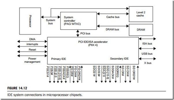
The PC (personal computer) is now a highly integrated system containing a microprocessor, an IDE systems controller and a PCI IDE/ISA accelerator, as illustrated in Figure 14.12. The IDE system controller provides the main interface between the processor and the level-2 cache, the DRAM, and the PCI bus. It is one of the most important devices in the system, since it ensures that data flow to and from the microprocessor in the correct way. The PCI bus links to interface devices, and also the PCI IDE/ISA accelerator (such as the PIIX4 device). The PCI IDE/ISA device then interfaces to other buses, such as IDE and ISA. The IDE interface has separate signals for both the primary and secondary IDE drives; these are electrically isolated, which allows drives to be swapped easily without affecting other ports.
The PCI IDE/ISA accelerator is a massively integrated device (the PIIX4 has 324 pins) and provides for an interface to other buses, such as USB and X-Bus. It also handles the interrupts from the PCI bus and the ISA bus. It thus has two integrated 82C59 interrupt controllers, which support up to
15 interrupts. The PCI IDE/ISA accelerator also handles DMA (direct memory access) transfers (on up to eight channels), and thus has two integrated 82C37 DMA controllers. Along with this, it has an integrated 82C54, which provides for the system timer, DRAM refresh signal, and the speaker tone output.
The IDE (or AT bus) is the de facto standard for most PC hard disks. It has the advantage over older-type interfaces that the controller is integrated into the disk drive, so the computer only has to pass high-level commands to the unit, and actual control can be achieved with the integrated controller. Several companies developed a standard command set for an AT attachment (ATA). Commands include: (1) read sector buffer, which reads contents of the controller’s sector buffer; (2) write sector buffer, which writes data to the controller’s sector buffer; (3) check for active; (4) read multiple sectors; (5) lock drive door. Control of the disk is achieved by passing a number of high-level commands through a number of I/O port registers.
(4) SCSI (small computer system interface) ports
Small computer system interface (SCSI) is a set of interface standards for physically connecting and transferring data between computers and peripheral devices, most commonly used for hard disks and tape drives, but able to connect a wide range of other devices, including scanners, and CD and DVD drives.
The SCSI standards define commands, protocols, and electrical and optical interfaces. Within a SCSI interface, there is an intelligent bus subsystem which can support multiple devices cooperating concurrently. Each device is assigned a priority. The main types of SCSI are:
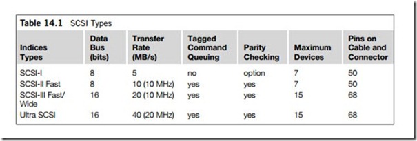
1. SCSI-I. SCSI-I transfers at rate of 5Mbps with an 8-bit data bus and seven devices per controller.
2. SCSI-II. SCSI-II supports SCSI-I and has one or more of the following features:
(a) Fast SCSI, which uses a synchronous transfer to give 10 Mbps transfer rate. The initiator and target initially negotiate to see whether they can both support synchronous transfer. If they can, they then go into a synchronous transfer mode.
(b) Fast and Wide SCSI-2, which doubles the data bus width to 16 bits to give 20 Mbps transfer rate.
(c) Fifteen devices per master device.
(d) Tagged command queuing (TCQ), which greatly improves performance and is supported by Windows, NetWare, and OS-2.
(e) Multiple commands sent to each device.
(f) Commands executed in whatever sequence will maximize device performance.
3. Ultra SCSI (SCSI-III). Ultra SCSI operates either as 8-bit or 16-bit with either 20 or 40 Mbps transfer rate (Table 14.1).
A SCSI bus is made of a host adapter connected to a number of SCSI units. Although all units connect to a common bus, only two units can transfer data at a time, either from one unit to another or from one unit to the host. The great advantage of this transfer mechanism is that it does not involve the microprocessor.
Each unit is assigned a SCSI-ID address. In the case of SCSI-I, this ranges from 0 to 7 (where 7 is normally reserved for a tape drive). The host adapter takes one of the addresses; thus a maximum of seven units can connect to the bus. Most systems allow the units to take any SCSI-ID address, but older systems used to require boot drives to be connected to a specific SCSI address. When the system is
initially booted, the host adapter sends out a start unit command to each SCSI unit. This allows each of the units to start in an orderly manner (and not overload the local power supply). The host will start with the highest-priority address (ID ¼ 7) and finishes with the lowest address (ID ¼ 0). Typically, the ID is set with a rotating switch selector or by three jumpers.
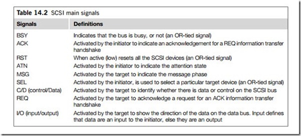
SCSI defines an initiator control and a target control. The initiator requests a function from a target, which then executes the function, as illustrated in Figure 14.13, where the initiator effectively takes over the bus for the time to send a command and the target executes the command and then contacts the initiator and transfers any data. The bus will then be free for other transfers. Table 14.2 gives the definitions of the main SCSI signals. Each of the control signals can be true or false, OR-tied driven or Non-OR-tied driven. In OR-tied driven mode, the driver does not drive the signal to the false state. In this case, the bias circuitry of the bus terminators pulls the signal false whenever it is released by the drivers at every SCSI device. If any driver is asserted, then the signal is true. The BSY, SEL, and RST signals are OR-tied. In the ordinary operation of the bus, the BSY and RST signals may be simulta- neously driven true by several drivers. However, in Non-OR-tied driven, the signal may be actively driven false. No signals other than BSY, RST, and D(PARITY) are driven simultaneously by two or more drivers.
The SCSI bus allows any unit to talk to any other unit, or the host to talk to any unit. Thus there must be some means of arbitration where units capture the bus. The main phases that the bus goes through are as follows:
1. Free bus. In this state, there are no units that either transfer data or have control of the bus. It is identified by deactivate SEL and BSY (both will be high). Thus, any unit can capture the bus.
2. Arbitration. In this state, a unit can take control of the bus and become an initiator. To do this, it activates the BSY signal and puts its own ID address on the data bus. After a delay, it tests the data
bus to determine whether a high-priority unit has put its own address on it. If it has, then it will allow the other unit access to the bus. If its address is still on it, then it asserts the SEL line. After a delay, it then has control of the bus.
3. Selection. In this state, the initiator selects a target unit to carry out a given function, such as reading or writing data. The initiator outputs the OR value of its SCSI-ID and the SCSI-ID of the target onto the data bus (e.g., if the initiator is 2 and the target is 5 then the OR-ed ID on the bus will be 00100100). The target then determines that its ID is on the data bus and sets the BSY line active. If this does not happen within a given time, then the initiator deactivates the SEL signal, and the bus will be free. The target determines that it is selected when the SEL signal and its SCSI-ID bit are active and the BSY and I/O signals are false. It then asserts the BSY signal within a selection abort time.
4. Reselection. When the arbitration phase is complete, the wining SCSI device asserts the BSY and SEL signals and has delayed at least a bus clear delay plus a bus settle delay. The wining SCSI device sets the DATA BUS to a value that is the logical OR of its SCSI-ID bit and the initiator’s CSI-ID bit. Sometimes, the target takes some time to reply to the initiator’s request. The initiator determines that it is reselected when the SEL and I/O signals and its SCSI-ID bit are true and the BSY signal is false. The reselected initiator then asserts the BSY signal within a selection abort time of its most recent detection of being reselected. An initiator does not respond to a reselection phase if other than two SCSI-ID bits are on the data bus. After the target detects that the BSY signal is true, it also asserts the BSY signal and waits a given time delay and then releases the SEL signal. The target may then change the I/O signal and the DATA BUS. After the reselected initiator detects the SEL signal is false, it releases the BSY signal. The target continues to assert the BSY signal until it gives up the SCSI bus.
5. Command. The command phase is used by the target to request command information from the initiator. The target asserts the C/D signal and negates the I/O and MSG signals during the REQ/ ACK handshake(s) of this phase. The format of the command descriptor block for 6-byte commands is: Byte 0 is operation code; Byte 1 is logical unit number (MSB, if required); Byte 2 is logic block address; Byte 3 is logic block address (LSB, if required); Byte 4 is transfer length (if required)/parameter list length (if required)/allocation length (if required); Byte 5 is control code.
6. Data. The data phase covers both the data-in and data-out phases. In the data-in phase, the target requests that data be sent to the initiator. For this purpose, it asserts the I/O signal and negates the C/ D and MSG signals during the REQ/ACK handshake(s) of the phase. In the data-out phase, it requests that data be sent from the initiator to the target. The target negates the C/D, I/O, and MSG signals during the REQ/ACK handshake(s) of this phase.
7. Message. The message phase covers both the message-out and message-in phases. The first byte transferred in either of these phases can be either a single-byte message or the first byte of a multiple-byte message. Multiple-byte messages are contained completely within a single message phase. The message system allows the initiator and the target to communicate over the interface connection. Each message can be one, two, or more bytes in length. In a single message phase, one or more messages can be transmitted (but a message cannot be split between multiple message phases).
8. Status. The status phase allows the target to request that status information be sent from the target to the initiator. The target asserts the C/D and I/O signals and negates the MSG signal during the REQ/ ACK handshake(s) of this phase. The status phase normally occurs at the end of a command (although in some cases it may occur before transferring the command descriptor block).
14.2.3 I/O connectors
Serial data communication implies that the bits of a character (or byte) are transmitted consecutively to a receiver that assembles the bits back into a character. Data rate, error checking, handshaking, and character framing (start and stop bits) are pre-defined and must correspond at both the transmitting and receiving terminals.
Both serial synchronous and asynchronous transmissions can be implemented with a series of Recommended Standards (RS), which usually define signal levels, maximum bandwidth, connector pinout, supported handshaking signals, drive capabilities, and electrical characteristics of the serial transmissions.
The following briefly describes some common serial transmission standards. All these interfaces accept a range of electrical and physical parameters and may even operate in excess of the specified standard. The full specification for each standard is available from almost any supplier of engineering documents.
(1) RS-232
In the RS-232 standard, data are sent as a time-series of bits. Both synchronous and asynchronous transmissions are supported by this standard. In addition to the data circuits, the standard defines a number of control circuits used to manage the connection between the DTE and DCE. Each circuit only operates in one direction; that is, signaling from a DTE to the connected DCE or the reverse. Since transmit data and receive data use separate circuits, the RS-232 interface can operate in a full duplex manner, supporting concurrent data flow in both directions. The standard does not define character framing within the data stream, or character encoding.
1. Voltage levels. The RS-232 standard defines the voltage levels that correspond to logical “1” and logical “0” levels for the data and the control signals. Valid data and control signals are plus or minus 3 to 15 V; however, the range near zero volts is not a valid RS-232 level. The standard specifies a maximum open-circuit voltage of 25 V: signal levels of ±5 V, ±10 V, ±12 V, and ±15 V are all commonly seen depending on the power supplies available within a device. RS-232 drivers and receivers must be able to withstand indefinite short-circuit to ground, or to any voltage level up to ±25 V. The slew rate, or how fast the signal changes between levels, is also controlled.
2. Connectors. The RS-232 standard specifies 20 different signal connections. Since most devices use only a few signals, smaller connectors can often be used. The standard recommended, but did not make mandatory, the D-subminiature 25-pin (DB-25) connector. In general, and according to the standard, terminals and computers have male connectors with DTE pin functions, and modems have female connectors with DCE pin functions. Other devices may have any combination of connector gender and pin definitions. Many terminals were manufactured with female terminals but were sold with a cable with male connectors at each end; the terminal with its cable satisfied the recommendations in the standard.
3. Cables. The RS-232 standard does not define a maximum cable length, but instead defines the maximum capacitance that a compliant drive circuit must tolerate. A widely used rule-of-thumb indicates that cables more than 50 feet (15 meters) long will have too much capacitance, unless special cables are used. By using low-capacitance cables, full speed communication can be maintained over distances of up to about 1000 feet. Other signal standards are better suited to longer distances.
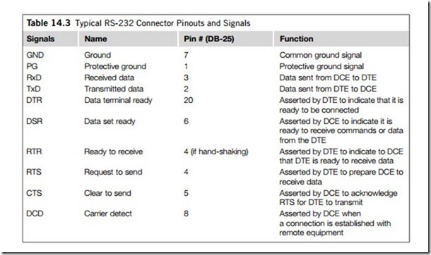
4. Pinouts and signals. Commonly used RS-232 pinouts and signals are given in Table 14.3. Note that only the DB-25 connector pinouts are given in Table 14.3. Other types of connector, DE-9 (TIA-574), EIA/TIA 561, and Yost, are not given in this table.
5. Conventions. For functional communication through a serial port interface, conventions of bit rate, character framing, communications protocol, character encoding, data compression, and error detection, not defined in the RS-232 standard, must be agreed to by both sending and receiving equipment. For example, consider the serial ports of the original IBM PC. This implementation used an 8250 UART (universal asynchronous receiver-transmitter) using asynchronous start-stop character formatting with 7 or 8 data bits per frame, usually ASCII character encoding, and data rates programmable between 75 bps and 115,200 bps. Data rates above 20,000 bps are out of the scope of the standard, although they are sometimes used in commercially manufactured equipment.
(2) RS-422
RS-422, unlike RS-232, is a differential interface that defines voltage levels, and driver and receiver electrical specifications. On this interface, logic levels are defined by the difference in voltage between a pair of outputs or inputs. In contrast, a single-ended interface, for example RS-232, defines the logic levels as the difference in voltage between a single signal and a common ground connection. Differential interfaces are typically more immune to noise or voltage spikes.
Differential interfaces also have greater drive capabilities, which allow for longer cable lengths. RS-422 is rated up to 10 Mbps and can have cabling 4000 feet long. It also defines driver and receiver electrical characteristics that will allow one driver and up to 32 receivers on the line at once. RS-422 signal levels range from 0 to þ5 V. RS-422 does not define a physical connector.
(3) RS-485
Similar to the RS-422 standard, RS-485 is also a differential interface, allowing cable lengths up to 4000 feet and data rates up to 10 Mbps. The signal levels are the same as those defined by RS-422, having electrical characteristics that allow for 32 drivers and 32 receivers to be connected to one line. This interface is ideal for multiple-drop or network environments. RS-485’s triple-state driver (not dual-state) will allow the electrical presence of the driver to be removed from the line. The driver is in a triple-state or high impedance condition when this occurs. Only one driver may be active at a time and the other driver(s) must be triple-stated.
The output modem-control signal “Request to Send (RTS)” controls the state of the driver. Some communication software packages refer to RS-485 as RTS enable or RTS block-mode transfer.
RS-485 can be cabled in two ways: two-wire and four-wire mode. Two-wire mode does not allow for full-duplex communication. Two-wire mode requires that data be transferred in only one direction at a time and the two transmit pins should be connected to the two receive pins (Txþ to Rxþ and Tx- to Rx-). Four-wire mode will allow full-duplex data transfers. RS-485 does not define a physical connector, a connector pinout, or a set of modem control signals.
(4) RS-499 and RS-530
Both RS-499 and RS-530 are similar to RS-422 and RS-485, in that they are differential interfaces, but these latest two standards provide a specified pinout defining a full set of modem-control signals that can be used for regulating flow control and line status. RS-449 is defined on a standard DB-37 (D- subminiature 37-pin) connector; RS-530 is backwards-compatible and replaces RS-449. RS-530 is defined on a DB-25 connector. These two interfaces do not define an electrical specification, but they do provide a means of selecting a standard cabling interface.
