DATA TRANSMISSION CONTROL DEVICES
Within a microprocessor chipset, a computer motherboard, or a multiple-core processor chipset, data signals are transferred internally using a parallel format: all the bits of a byte or a memory word are exchanged simultaneously among registers, buses, ASIC etc. However, for the data to be communicated over a serial channel, it must be converted from parallel to a serial bit stream. Some special hardware units including circuits or other devices are therefore required to control the mutual trans- lations between serial and parallel formats.
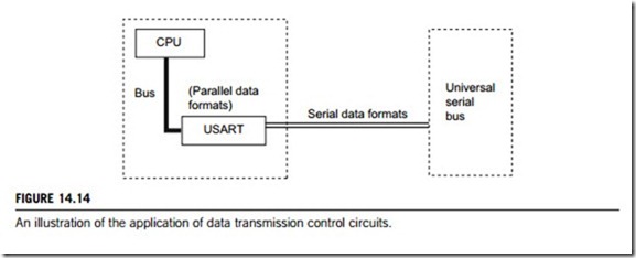
This section lists a group of important hardware units for digital data transmission control. One of these is the universal receiver-transmitter, which comes in three types: universal asynchronous receiver-transmitter (UART), universal synchronous receiver-transmitter (USRT), and universal synchronous/asynchronous receiver-transmitter (USART). Other hardware units for data transmission control are multiplexers and modems. All of them may be built into a computer or programmable controller, added as components of an I/O interface board, or may consist of a single ASIC chip. Figure 14.14 shows an example application.
Universal asynchronous receiver-transmitter (UART)
A UART is a microchip or integrated circuit with a hardcoded program that controls the interface between a computer or programmable controller and its attached serial devices. Specifically, it provides the computer with an RS-232-specified DTE interface so that it can “talk” to and exchange data with modems and other serial devices. UART is commonly used with RS-232 for embedded systems communications. Many microprocessor chips thus provide functionality to convert UART to RS-232 signals.
As part of this interface, the main functions of a UART include the following: (1) convert the bytes received from the computer along parallel circuits into a single-serial bit-stream for outbound
transmission; (2) on inbound transmission, convert the serial bit-stream into the bytes that the computer handles; (3) add a parity bit (if it has been selected) on outbound transmissions and check the parity of incoming bytes (if selected) and discard the parity bit; (4) add start and stop delineators on outbound data and strip them from inbound transmissions; (5) handle interrupts from serial devices with special ports such as keyboard and mouse; (6) possibly handle other kinds of interrupt and device management that require coordinating the computer’s speed of operation with device speeds.
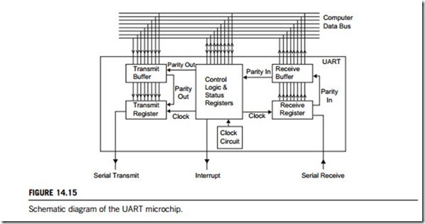
Figure 14.15 is a schematic diagram of a UART microchip, which usually contains the following components: (1) transmit and receive buffer, (2) transmit and receive register, (3) data bus buffer, (4) control logics, and (5) clock circuit. The control logic circuitry of UART has a number of internal registers that contain all the relevant status information for the device. These registers are generally mapped onto the computer’s memory and can be accessed from the main CPU. The key is that each UART contains a shift register that is the fundamental method of conversion between serial and parallel forms.
The word asynchronous indicates that a UART recovers character timing information from the data stream, using designated start and stop bits to indicate the framing of each character. By convention, teletype-style UARTs send a start bit, 5 8 data bits, least-significant-bit first, an optional parity bit, and then a stop bit. The start bit is the opposite polarity of the data-line’s normal state. The stop-bit is the data-line’s normal state, and provides a space before the next character can start. In mechanical teletypes, the stop bit was often stretched to two bit times to give the mechanism more time to finish printing a character. A stretched stop bit also helps resynchronization. The parity bit can either make the number of bits odd or even, or it can be omitted. Odd parity is more reliable because it ensures that there will always be a data transition, and this permits many UARTs to resynchronize.
As shown in Figure 14.15, most UARTs are designed to assert an interrupt line when data have been received. This enables the CPU to run an interrupt service routine that removes data from the volatile
registers and buffers in the UART and places them into a more stable area of general-purpose computer memory.
Universal synchronous receiver-transmitter (USRT)
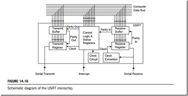
For synchronous transmission schemes, the USRT is used for conversion between serial and parallel data formats. A schematic is shown in Figure 14.16. In principle, the USRT is similar to the UART, except that the incoming data are clocked into the receive register with a signal that is derived (extracted) from the data themselves.
In synchronous transmission, the clock data are recovered separately from the data stream and no start/stop bits are used. This improves the efficiency of transmission on suitable channels; more of the bits sent are data. Therefore, the USRT is a circuit capable of receiving and sending data without requiring a start or a stop bit code, unlike the asynchronous procedure mentioned in the last subsection.
Universal synchronous/asynchronous receiver-transmitter (USART)
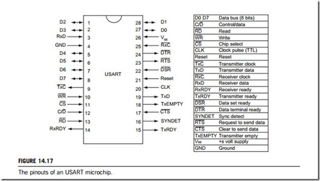
The universal synchronous asynchronous receiver-transmitter (USART) microchip is composed of some logic circuit, connected by an internal data bus with a microprocessor or a CPU. Figure 14.17 is a diagram of the pinouts of a USART microchip.
The USART is programmable, meaning the microprocessor or CPU can control its mode of operation using data bus control and command words. The USART microchip is typically architected into the following five control circuits:
1. Read/write control. The read/write control logic circuit accepts control signals from the control bus and command or control words from the data bus. The USART is set to an idle state by the RESET
signal or control word. When the USART is in idle state, a new set of control words is required to program it for the applicable interface. The read/write control logic circuit receives a clock signal (CLK) that is used to generate internal device timing.
2. Modem control. The modem control logic circuit generates or receives four control or status signals (DSR, DTR, RTS, and CTS) used to simplify modem interfaces.
3. Baud rate generator (BRG). The BRG supports both asynchronous and synchronous modes of the USART. It is a dedicated 8-bit or more baud rate generator. The SPBRG register controls the period of a free-running 8-bit timer. In asynchronous mode, bit BRGH in the TXSTA register also controls the baud rate. In synchronous mode, bit BRGH is ignored.
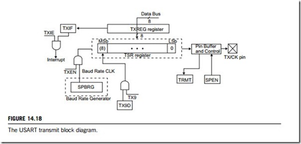
4. Transmit buffer/transmit control. The transmit control logic converts the data bytes stored in the transmit buffer into an asynchronous bit stream. The transmit control logic inserts the applicable start/stop and parity bits into the stream to provide the programmed protocol. A start bit is used to alert the output device, a printer for instance, to get ready for the actual character (bit). The signal is sent just before the beginning of the actual character coming down the line. A stop bit is sent to indicate the end of transmission. The parity bit is used as a means to detect errors; odd or even parity may be used. Figure 14.18 is the transmit block diagram for a USART microchip.
5. Receive buffer/receive control. The receive control logic accepts the input bit stream and strips the
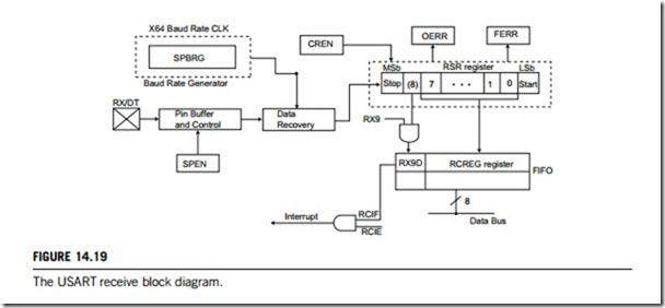
protocol signals from the data bits. The data bits are converted into parallel bytes and stored in the receive buffer until transmitted to the microprocessor. Figure 14.19 is the receive block diagram for a USART microchip.
USART can be configured into asynchronous (full duplex), synchronous-master (half duplex), and synchronous-slave (half duplex) modes. They are discussed below in reference to Figures 14.18 and 14.19.
(1) USART asynchronous mode
In this mode, USART uses standard nonreturn-to-zero (NRZ) format (one start bit, eight or nine data bits, and one stop bit). The most common data format is 8 bits (of course there can be more bits than 8). An on-chip dedicated 8-bit baud rate generator can be used to derive standard baud rate frequencies from the oscillator. USART transmits and receives the LSb first. The transmitter and receiver are functionally independent but use the same data format and baud rate. The baud rate generator produces a clock either x16 or x64 of the bit shift rate, depending on the BRGH bit in the TXSTA register. Parity is not supported by the hardware, but can be implemented in software (stored as the ninth data
bit). Asynchronous mode is stopped during SLEEP, and selected by clearing the SYNC bit in the TXSTA register.
The USART asynchronous module consists of the following hardware elements: baud rate generator, sampling circuit, asynchronous transmitter, and asynchronous receiver.
(a) USART asynchronous transmitter
The USART transmitter block diagram is shown in Figure 14.18. The heart of the transmitter is the (serial) transmit shift register (TSR). This obtains its data from the read/write transmit buffer, TXREG. The TXREG register is loaded with data in software. The TSR register is not loaded until the STOP bit has been transmitted from the previous load. As soon as this occurs, the TSR is loaded with new data from the TXREG register (if available). Once the TXREG register transfers the data to the TSR register (occurs in one timing cycle), the TXREG register is empty and the TXIF flag bit is set. This interrupt can be enabled/disabled by setting/clearing the TXIE enable bit. The TXIF flag bit will be set regardless of the state of the TXIE enable bit and cannot be cleared in software, but will reset only when new data are loaded into the TXREG register. While the TXIF flag bit indicates the status of the TXREG register, the TRMT bit in the TXSTA register shows the status of the TSR register. The TRMT status bit is a read-only bit that is set when the TSR register is empty. No interrupt logic is tied to this bit, so the user has to poll this bit to determine whether the TSR register is empty.
Transmission is enabled by setting the TXEN enable bit in the TXSTA register. Actual transmission will not occur until the TXREG register has been loaded with data and the baud rate generator (BRG) has produced a shift clock (Figure 14.18). Transmission can also be started by first loading the TXREG register and then setting the TXEN enable bit. Normally, when transmission is first started, the TSR register is empty, so a transfer to the TXREG register will result in an immediate transfer to TSR, resulting in an empty TXREG. A back-to-back transfer is thus possible.
(b) USART asynchronous receiver
The receiver block diagram is shown in Figure 14.19. The data are received on the RX/DT pin and drive the data recovery block. This is actually a high-speed shifter operating at x16 times the baud rate; whereas the main receive serial shifter operates at the bit rate or at 16 MHz.
Once asynchronous mode is selected, reception is enabled by setting the CREN bit in the RCSTA register. The heart of the receiver is the (serial) receive shift register (RSR). After sampling the RX/TX pin for the STOP bit, the received data in the RSR are transferred to the RCREG register (if it is empty). If the transfer is complete, the RCIF flag bit is set. The actual interrupt can be enabled/ disabled by setting/clearing the RCIE enable bit. The RCIF flag bit is a read-only bit that is cleared by the hardware, when the RCREG register has been read and is empty. The RCREG is a double-buffered register, that is, it is a two-deep FIFO (first-in-first-out). It is possible for two bytes of data to be received and transferred to the RCREG FIFO and a third byte to begin shifting to the RSR register. On the detection of the STOP bit of the third byte, if the RCREG register is still full then the overrun error bit, OERR (RCSTA), will be set, and the word in the RSR will be lost. The RCREG register can be read twice to retrieve the two bytes in the FIFO. The OERR bit has to be cleared in software by resetting the receive logic (the CREN bit is cleared and then set). If the OERR bit is set, transfers from the RSR register to the RCREG register are inhibited, so it is essential to clear the OERR bit if it is set.
The framing error bit, FERR (RCSTA), is set if a stop bit is detected as a low level. The FERR bit and the ninth receive bit are buffered in the same way as the received data. Reading the RCREG will load the RX9D and FERR bits with new values, therefore it is essential for the user to read the RCSTA register before reading the next RCREG register so as not to lose the old (previous) infor- mation in the FERR and RX9D bits.
(2) USART synchronous master mode
In synchronous master mode, the data are transmitted in a half-duplex manner, in which transmission and reception do not occur at the same time. When transmitting data, reception is inhibited and vice versa.
Synchronous mode is entered by setting the SYNC bit in the TXSTA register. In addition, the SPEN enable bit in the RCSTA register is set to configure the TX/CK and RX/DT I/O pins to CK (clock) and DT (data) lines, respectively. The master mode indicates that the processor transmits the master clock on the CK line. The master mode is entered by setting the CSRC bit in the TXSTA register.
(a) USART synchronous master transmission
The USART transmitter block diagram is shown in Figure 14.18. The heart of the transmitter is the (serial) transmit shift register (TSR), which obtains its data from the read/write transmit buffer register TXREG. The TXREG register is loaded with data in software. The TSR register is not loaded until the last bit has been transmitted from the previous load, at which point, the TSR is loaded with new data from the TXREG (if available). Once the TXREG register transfers the data to the TSR register, it becomes empty and the TXIF interrupt flag bit is set. The interrupt can be set into enabled/disabled by setting/clearing enable the TXIE bit. The TXIF flag bit will be set regardless of the state of the TXIE enable bit and cannot be cleared in software. It will reset only when new data are loaded into the TXREG register.
While the TXIF flag bit indicates the status of the TXREG register, the TRMT bit in the TXSTA register shows the status of the TSR register. The TRMT bit is a read-only bit that is set when the TSR is empty. No interrupt logic is tied to this bit, so the user has to poll it to determine whether the TSR register is empty. The TSR is not mapped in data memory so it is not available to the user.
(b) USART synchronous master reception
Once synchronous mode is selected, reception is enabled by setting either the SREN bit or the CREN bit in the RCSTA register. Data are sampled on the RX/DT pin on the falling edge of the clock. If the SREN bit is set, then only a single word is received. If the CREN bit is set, the reception is continuous until it is cleared. If both bits are set, then the CREN bit takes precedence. After clocking the last serial data bit, the received data in the receive shift register (RSR) are transferred to the RCREG register (if it is empty). When the transfer is complete, the RCIF interrupt flag bit is set. The actual interrupt can be enabled/disabled by setting/clearing the RCIE enable bit. The RCIF flag bit is a read-only bit that is cleared by the hardware, in this case, when the RCREG register has been read and is empty. The RCREG is a double-buffered register, which means that it is a two-deep FIFO (first-in-first-out). It is possible for two bytes of data to be received and transferred to the RCREG register by FIFO and a third byte to begin shifting into the RSR register.
On the clocking of the last bit of the third byte, if the RCREG register is still full then the overrun error bit will be set.
(3) USART synchronous slave mode
Synchronous slave mode differs from the synchronous master mode in that the shift clock is supplied externally at the TX/CK pin (instead of being supplied internally in master mode). This allows the device to transfer or receive data while in SLEEP mode. Slave mode is entered by clearing the CSRC bit in the TXSTA register.
(a) USART synchronous slave transmit
The transmit operations of both the synchronous master and slave modes are identical except in the case of the SLEEP mode.
If two words are written to the TXREG register and then the SLEEP instruction is executed, the following will occur: (1) The first word will immediately transfer to the TSR register and transmit.
(2) The second word will remain in the TXREG register. (3) The TXIF flag bit will not be set. (4) When the first word has been shifted out of TSR, the TXREG register will transfer the second word to the TSR and the TXIF flag bit will now be set. (5) If the TXIE enable bit is set, the interrupt will wake the chip from SLEEP and if the global interrupt is enabled, the program will branch to the interrupt vector.
(b) USART synchronous slave reception
The receive operations of both the synchronous master and slave modes are identical except in the case of the SLEEP mode. Also, bit SREN is a do-not-care in slave mode.
If receive is enabled, by setting the CREN bit, before the SLEEP instruction, then a word may be received during SLEEP. On completely receiving the word, the RSR register will transfer the data to the RCREG register and if the RCIE enable bit is set, the interrupt generated will wake the chip from SLEEP. If the global interrupt is enabled, the program will branch to the interrupt vector.
Bit-oriented protocol circuits
Bit-oriented protocols represent a class of data-link layer communication protocols that can transmit frames regardless of frame content. Unlike byte-oriented protocols, bit-oriented protocols provide full- duplex operation and are more efficient and reliable. However, the byte-oriented protocols use a specific character from the user character set to delimit frames in data-link communications. Today, byte-oriented protocol circuits have largely been replaced by bit-oriented protocols.
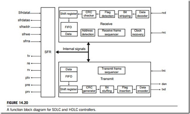
In current applications, there are two types of controller that can perform the bit-oriented protocol: the SDLC (synchronous data-link control) controller and the HDLC (high-level data-link control) controller. Figure 14.20 is a block diagram for both of these.
(1) SDLC controller
The SDLC controller is a bit-oriented protocol that presupposes an IBM protocol for use in a system network architecture (SNA) environment.
It supports a variety of link types and topologies, and can be used with point-to-point and multi- point links, bounded and unbounded media, half-duplex and full-duplex transmission facilities, and circuit-switched and packet-switched networks.
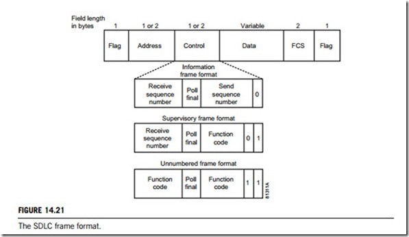
The SDLC frame, shown in Figure 14.21, is bounded by a unique flag pattern. The address field always contains the address of the secondary involved in the current communication. Because the primary is either the communication source or destination, there is no need to include its address: it is already known by all secondaries. The control field uses three different formats, depending on the type of SDLC frame used. They are described as follows:
(a) Information (I) frames. These frames carry upper-layer and some control information. Send and receive sequence numbers and the poll final (P/F) bit perform flow and error control. The send sequence number refers to the number of the frame to be sent next. The receive sequence number provides the number of the frame to be received next. Both sender and receiver maintain send and receive sequence numbers. The primary uses the P/F bit to tell the secondary whether it requires an immediate response, and the secondary then uses this bit to tell the primary whether the current frame is the last in its current response.
(b) Supervisory (S) frames. These frames provide control information. They request and suspend transmission, report on status, and acknowledge the receipt of I-frames. They do not have an information field.
(c) Unnumbered (U) frames. These frames, as the name suggests, are not sequenced, and are used for control purposes, for example, to initialize secondaries. Depending on the function of the unnumbered frame, its control field is 1 or 2 bytes. Some unnumbered frames have an information field.
The frame check sequence (FCS) precedes the ending flag delimiter. This is usually a cyclic redundancy check (CRC) calculation remainder. The CRC calculation is redone in the receiver. If the result differs from the value in the sender’s frame, an error is assumed.
(2) HDLC controller
The HDLC controller is an ISO communications protocol used in X.25 packet switching networks. It is a bit-oriented data-link control procedure under which all data transfer takes place in frames. Each frame ends with a frame check sequence for error detection.
HDLC shares the frame format of SDLC, and HDLC fields provide the same functionality as those in SDLC. HDLC also supports synchronous, full-duplex operation. HDLC differs from SDLC in several minor ways. First, HDLC has an option for a 32-bit or more checksum, and it does not support the loop or hub go-ahead configurations.
The major difference between the two is that SDLC supports only one transfer mode, while HDLC supports three. The three HDLC transfer modes are as follows:
(a) Normal response mode (NRM). This transfer mode is used by SDLC. In this mode, secondaries cannot communicate with a primary until the primary has given permission.
(b) Asynchronous response mode (ARM). This transfer mode allows secondaries to initiate communication with a primary without receiving permission.
(c) Asynchronous balanced mode (ABM). ABM introduces the combined node. A combined node can act as a primary or a secondary, depending on the situation. All ABM communication is between multiple combined nodes. In ABM environments, any combined station may initiate data transmission without permission from any other station.
Multiplexers
A multiplexer, sometimes simply referred to as “mux”, is a device that selects between a number of input signals. In its simplest form, it will have two signal inputs, one input control, and one output. An everyday example of a multiplexer is the source selection control on a home stereo unit.
Multiplexers are used in building digital semiconductors such as CPUs and graphics controllers. In these applications, the number of inputs is generally a multiple of 2 (2, 4, 8, 16, etc.), the number of outputs is either 1 or a relatively smaller multiple of 2, and the number of control signals is related to the combined number of inputs and outputs. For example, a 2-input, 1-output multiplexer requires only one control signal to select the input, while a 16-input, 4-output multiplexer requires four control signals to select the input and two to select the output.
They are mainly categorized on the basis of the working mechanisms described in subsection
14.1.2. Of the available types, the time-division multiplexer is more complex, and the digital multi- plexer is more important in applications.
(1) Digital multiplexer
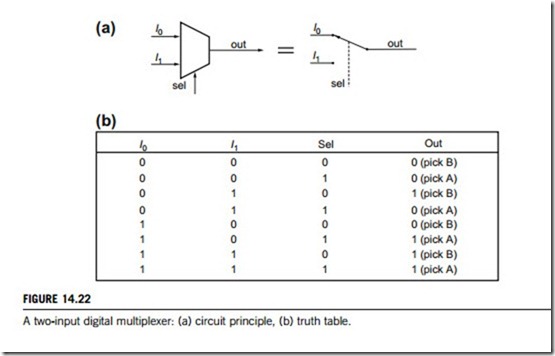
In the designations of digital integrated circuits, the multiplexer is a device that has multiple input streams and only one output stream. It forwards one of the input streams to the output stream based on the values of one or more selection inputs or control inputs. For example, a digital multiplexer with two inputs is a simple connection of logic gates whose output is either input I0 or input I1 depending on the value of a third input Sel which selects the input. Its Boolean equation is “Out ¼ (I0 and Sel) or (I1 and not Sel)”. The logic of this multiplexer can be expressed as Figure 14.22(a), and its truth table is given in Figure 14.22(b).
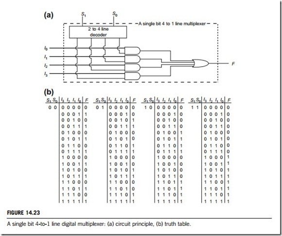
Larger digital multiplexers are also common. Figure 14.23 is a single bit 4-to-1 line digital multiplexer. Its logic is also expressed by the circuit diagram in Figure 14.23(a), and the truth table in Figure 14.23(b).
Conversely, demultiplexers take one data input and a number of selection inputs, and they have several outputs. They forward the data input to one of the outputs, depending on the values of the selection inputs. Demultiplexers are sometimes convenient for designing general-purpose logic, because if the demultiplexer’s input is always true, the demultiplexer acts as a decoder. This means that any function of the selection bits can be constructed by logically OR-ing the correct set of outputs.
(2) Time-division multiplexer
Time-division multiplexers (TDMs) share transmission time on an information channel among many data sources. Performance specifications for TDMs include number of channels, maximum data rate, wavelength range, operating voltage, optical output, electrical output, data transmission type, and data interface. Additional features may also be available.
One of the key factors in choosing a TDM is the selection of the transfer mode to be used. In synchronous transfer mode, data signals are sent at precise intervals that are regulated by a system clock. Additional start and stop pulses are not required. Asynchronous transfer mode (ATM) is a connection-oriented protocol that uses very short, fixed-length (53 bytes) packets called cells to carry voice, data, and video signals. By using a standard cell size, ATM can use software for data switching, and so can route and switch traffic at higher speeds. An asynchronous and/or synchronous time division multiplexer is capable of both asynchronous and synchronous transfer modes.
There are three cable choices for TDMs. Single-mode optical-fiber cable allows only one mode to propagate. The fiber has a very small core diameter of approximately 8 mm. It permits signal trans- mission at extremely high bandwidths and allows very long transmission distances. Multimode fiber- optic cable supports the propagation of multiple modes. It may have a typical core diameter of 50 mm with a refractive index that is graded or stepped, so allowing use of inexpensive LED light sources. Connector alignment and coupling is less critical than with single-mode fiber. Distances of trans- mission and transmission bandwidth are also less than with single-mode fiber due to dispersion. Single-mode/multimode time-division multiplexers can be used with both single-mode and multimode cable types.
